


PIC16(L)F1507
Data Sheet
20-Pin Flash, 8-Bit Microcontrollers
2011 Microchip Technology Inc. Preliminary DS41586A

Note the following details of the code protection feature on Microchip devices:
• Microchip products meet the specification contained in their particular Microchip Data Sheet.
• Microchip believes that its family of products is one of the most secure families of its kind on the market today, when used in the
intended manner and under normal conditions.
• There are dishonest and possibly illegal methods used to breach the code protection feature. All of these methods, to our
knowledge, require using the Microchip products in a manner outside the operating specifications contained in Microchip’s Data
Sheets. Most likely, the person doing so is engaged in theft of intellectual property.
• Microchip is willing to work with the customer who is concerned about the integrity of their code.
• Neither Microchip nor any other semiconductor manufacturer can guarantee the security of their code. Code protection does not
mean that we are guaranteeing the product as “unbreakable.”
Code protection is constantly evolving. We at Microchip are committed to continuously improving the code protection features of our
products. Attempts to break Microchip’s code protection feature may be a violation of the Digital Millennium Copyright Act. If such acts
allow unauthorized access to your software or other copyrighted work, you may have a right to sue for relief under that Act.
Information contained in this publication regarding device
applications and the like is provided only for your convenience
and may be superseded by updates. It is your responsibility to
ensure that your application meets with your specifications.
MICROCHIP MAKES NO REPRESENTATIONS OR
WARRANTIES OF ANY KIND WHETHER EXPRESS OR
IMPLIED, WRITTEN OR ORAL, STATUTORY OR
OTHERWISE, RELATED TO THE INFORMATION,
INCLUDING BUT NOT LIMITED TO ITS CONDITION,
QUALITY, PERFORMANCE, MERCHANTABILITY OR
FITNESS FOR PURPOSE. Microchip disclaims all liability
arising from this information and its use. Use of Microchip
devices in life support and/or safety applications is entirely at
the buyer’s risk, and the buyer agrees to defend, indemnify and
hold harmless Microchip from any and all damages, claims,
suits, or expenses resulting from such use. No licenses are
conveyed, implicitly or otherwise, under any Microchip
intellectual property rights.
Trademarks
The Microchip name and logo, the Microchip logo, dsPIC,
K
EELOQ, KEELOQ logo, MPLAB, PIC, PICmicro, PICSTART,
32
PIC
logo, rfPIC and UNI/O are registered trademarks of
Microchip Technology Incorporated in the U.S.A. and other
countries.
FilterLab, Hampshire, HI-TECH C, Linear Active Thermistor,
MXDEV, MXLAB, SEEVAL and The Embedded Control
Solutions Company are registered trademarks of Microchip
Technology Incorporated in the U.S.A.
Analog-for-the-Digital Age, Application Maestro, chipKIT,
chipKIT logo, CodeGuard, dsPICDEM, dsPICDEM.net,
dsPICworks, dsSPEAK, ECAN, ECONOMONITOR,
FanSense, HI-TIDE, In-Circuit Serial Programming, ICSP,
Mindi, MiWi, MPASM, MPLAB Certified logo, MPLIB,
MPLINK, mTouch, Omniscient Code Generation, PICC,
PICC-18, PICDEM, PICDEM.net, PICkit, PICtail, REAL ICE,
rfLAB, Select Mode, Total Endurance, TSHARC,
UniWinDriver, WiperLock and ZENA are trademarks of
Microchip Technology Incorporated in the U.S.A. and other
countries.
SQTP is a service mark of Microchip Technology Incorporated
in the U.S.A.
All other trademarks mentioned herein are property of their
respective companies.
© 2011, Microchip Technology Incorporated, Printed in the
U.S.A., All Rights Reserved.
Printed on recycled paper.
ISBN: 978-1-61341-342-5
Microchip received ISO/TS-16949:2002 certification for its worldwide
headquarters, design and wafer fabrication facilities in Chandler and
Tempe, Arizona; Gresham, Oregon and design centers in California
and India. The Company’s quality system processes and procedures
are for its PIC
devices, Serial EEPROMs, microperipherals, nonvolatile memory and
analog products. In addition, Microchip’s quality system for the design
and manufacture of development systems is ISO 9001:2000 certified.
®
MCUs and dsPIC® DSCs, KEELOQ
®
code hopping
DS41586A-page 2 Preliminary 2011 Microchip Technology Inc.

PIC16(L)F1507
20-Pin Flash, 8-Bit Microco ntr ollers
High-Performance RISC CPU:
• C Compiler Optimized Architecture
• Only 49 Instructions
• Up to 3.5 Kbytes Linear Program Memory
Addressing
• Up to 128 bytes Linear Data Memory Addressing
• Operating Speed:
- DC – 20 MHz clock input
- DC – 125 ns instruction cycle
• Interrupt Capability with Automatic Context
Saving
• 16-Level Deep Hardware Stack with Optional
Overflow/Underflow Reset
• Direct, Indirect and Relative Addressing modes:
- Two full 16-bit File Select Registers (FSRs)
- FSRs can read program and data memory
Flexible Oscillator Struc ture:
• 16 MHz Internal Oscillator Block:
- Factory calibrated to 1%, typical
- Software selectable frequency range from
16 MHz to 31 kHz
• 31 kHz Low-Power Internal Oscillator
• Three External Clock modes up to 20 MHz
Special Microcontroller Features:
• Operating Voltage Range:
- 1.8V to 3.6V (PIC16LF1507)
- 2.3V to 5.5V (PIC16F1507)
• Self-Programmable under Software Control
• Power-on Reset (POR)
• Power-up Timer (PWRT)
• Programmable Low-Power Brown-Out Reset
(LPBOR)
• Extended Watch-Dog Timer (WDT):
- Programmable period from 1 ms to 256s
• Programmable Code Protection
• In-Circuit Serial Programming™ (ICSP™) via two
pins
• Enhanced Low-Voltage Programming (LVP)
• Power-Saving Sleep mode
Low-Power Features (PIC16LF1507):
• Standby Current:
- 20 nA @ 1.8V, typical
• Operating Current:
-30A per MHz @ 1.8V, typical
• Low-Power Watchdog Timer Current:
- 300 nA @ 1.8V, typical
Analog Features:
• Analog-to-Digital Converter (ADC):
- 10-bit resolution
- Up to 12 channels
- Auto acquisition capability
- Conversion available during Sleep
- FVR available as channel
• Voltage Reference module:
- Fixed Voltage Reference (FVR) with 1.024V,
2.048V and 4.096V output levels
Peripheral Features:
• 17 I/O Pins and 1 Input-only Pin:
- High current sink/source 25 mA/25 mA
- Individually programmable weak pull-ups
- Individually programmable
interrupt-on-change (IOC) pins
• Timer0: 8-Bit Timer/Counter with 8-Bit
Programmable Prescaler
• Enhanced Timer1:
- 16-bit timer/counter with prescaler
- External Gate Input mode
• Timer2: 8-Bit Timer/Counter with 8-Bit Period
Register, Prescaler and Postscaler
• Four 10-bit PWM modules
• Two Configurable Logic Cell (CLC) modules:
- 22 individual input sources
- Four inputs and 16 selectable input sources
per module
- Software selectable logic functions including:
AND/OR/XOR/D Flop/D Latch/SR/JK
- External and internal inputs/outputs
- Operation while in Sleep
• Numerically Controlled Oscillator (NCO):
- 20-bit Accumulator
- 16-bit Increment
- Linear frequency control
- High-speed clock input
- Selectable Output modes
- Fixed Duty Cycle (FDC) mode
- Pulse Frequency (PF) mode
• Complementary Waveform Generator (CWG):
- 6 selectable signal sources
- Selectable falling and rising edge dead-band
control
- Polarity control
- 2 auto-shutdown sources
- Multiple input sources: PWM, CLC, NCO
2011 Microchip Technology Inc. Preliminary DS41586A-page 3

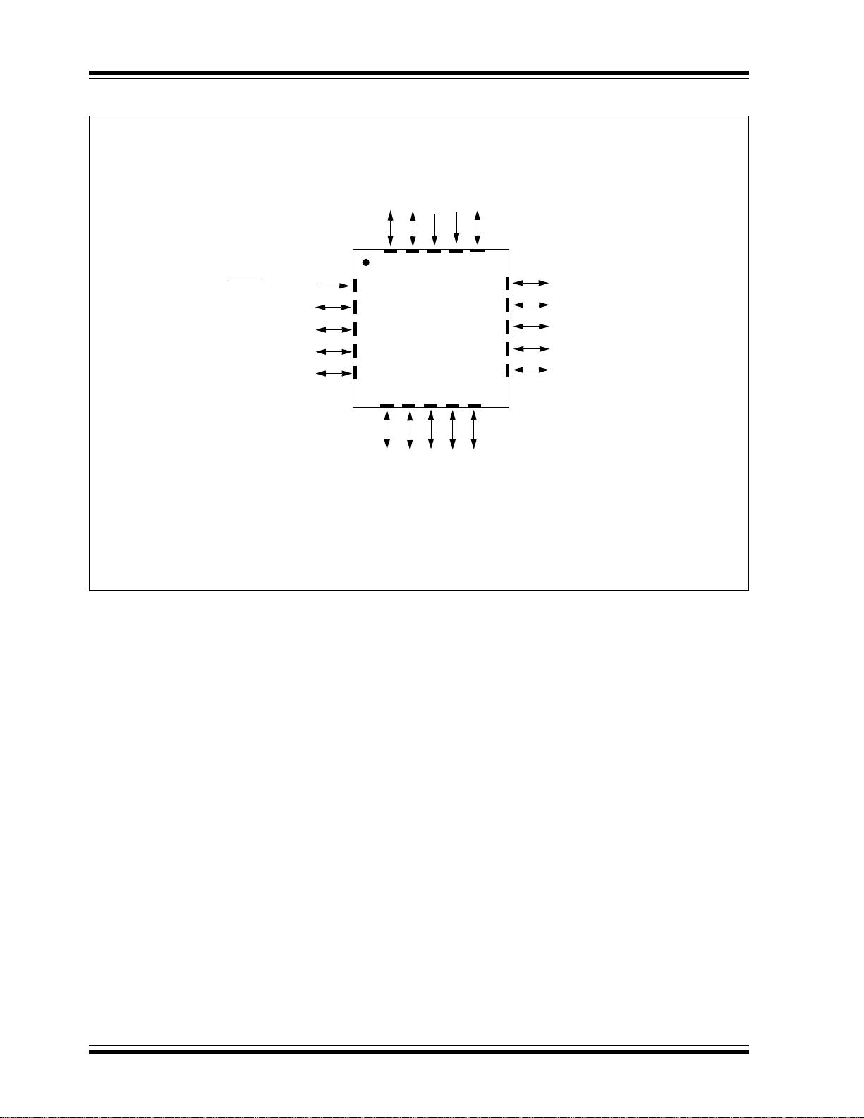
PIC16(L)F1507 Family Types
PIC16F1507
PIC16LF1507
1
2
3
4
14
13
12
11
5
6
7
10
9
8
VDD
RA5
RA4
MCLR
/VPP/RA3
RC5
RC4
V
SS
RA0/ICSPDAT
RA1/ICSPCLK
RA2
RC0
RC1
RC2
RC3
PDIP, SOIC, SSOP
Note: See Tab le 1 for location of all peripheral functions.
18
17
16
15
20
19
RC6
RC7
RB7
RB4
RB5
RB6
PIC16(L)F1507
Program
Device
PIC16F1507
PIC16LF1507
Note1: One pin is input-only.
Memory Flash
(words)
2048 128 18 12 2/1 4 1 2 1
SRAM
(bytes)
I/O
10-bit A/D
(1)
(ch)
Timers
8/16-bit
PWM CWG CLC NCO
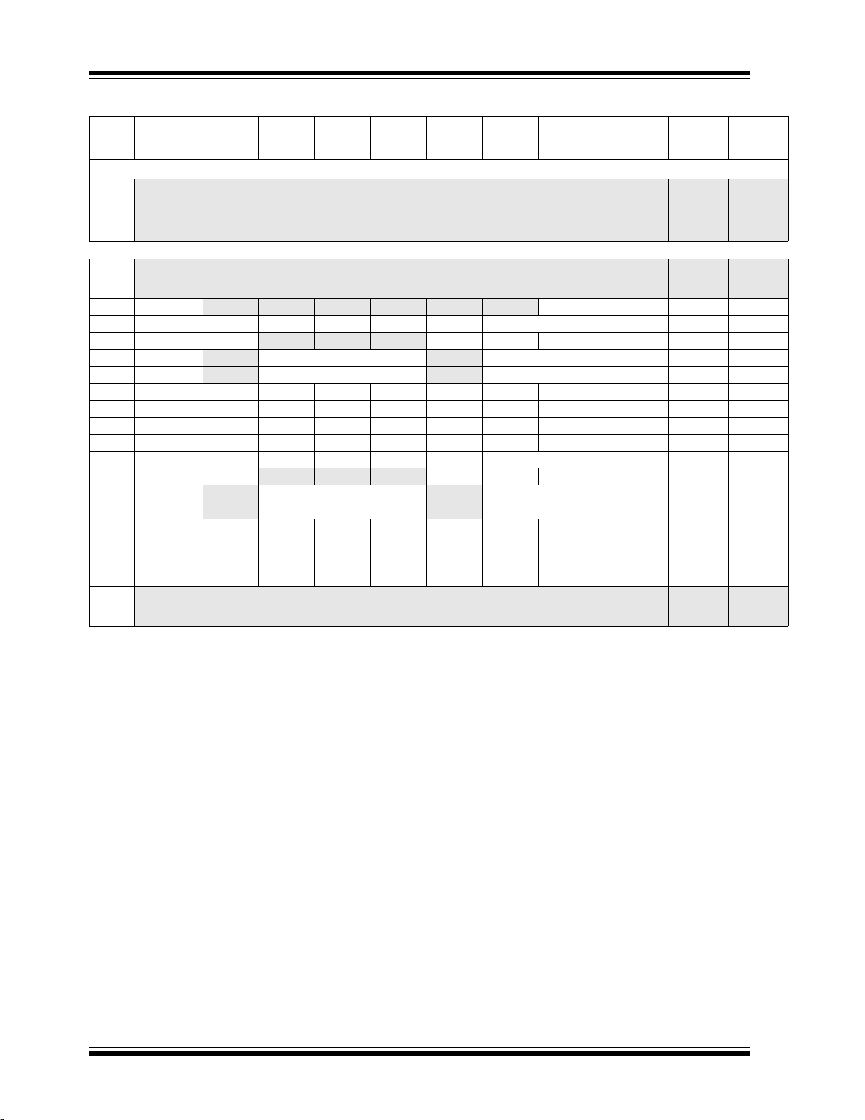
FIGURE 1: 20-PIN PDIP, SOIC, SSOP PACKAGE DIAGRAM FOR PIC16(L)F1507
2011 Microchip Technology Inc. Preliminary DS41586A-page 4
PIC16(L)F1507
PIC16
F1507
PIC16LF1507
QFN 4x4
Note: See Tab le 1 for location of all peripheral functions.
15
RA1/ICSPCLK
RA2
RC0
RC1
RC2
11
12
13
14
6
7
RC7
RB7
RB4
RB5
RB6
8
9
10
2
3
1
1819
20
1617
5
4
VDD
RA5
RA4
MCLR/VPP/RA3
RC5
RC4
RC3
RC6
VSS
RA0/ICSPDAT
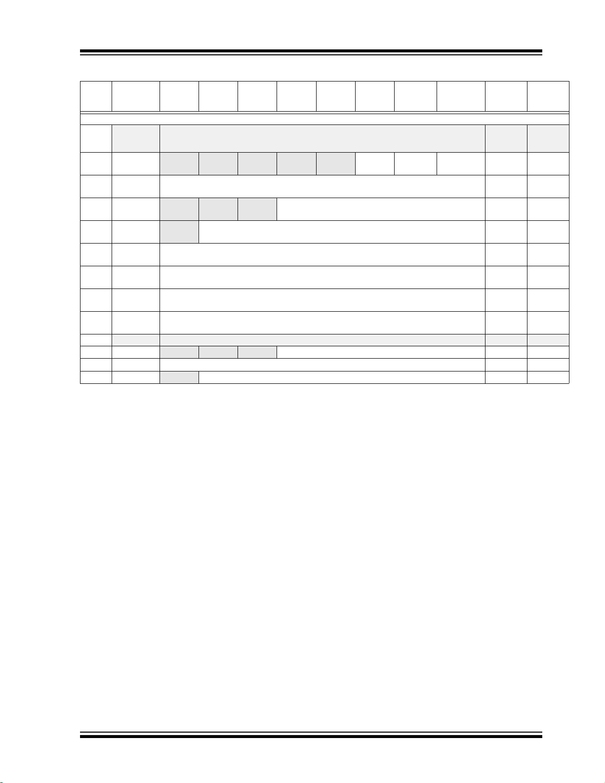
FIGURE 2: 20-PIN QFN PACKAGE DIAGRAM FOR PIC16(L)F1507
DS41586A-page 5 Preliminary 2011 Microchip Technology Inc.

TABLE 1: 20-PIN ALLOCATION TABLE (PIC16(L)F1507)
PIC16(L)F1507
I/O
20-Pin PDIP/SOIC/SSOP
RA0 19 16 AN0 — — — — — — IOC Y ICSPDAT
RA1 18 15 AN1 VREF+ — — — — — IOC Y ICSPCLK
RA2 17 14 AN2 — CWG1FLT — CLC1
RA3 4 1 — — — — CLC1IN0 — — IOC Y MCLR
RA4 3 20 AN3 — — — — T1G — IOC Y CLKOUT
RA5 2 19 — — — NCO1CLK — T1CKI — IOC Y CLKIN
RB4 13 10 AN10 — — — — — — IOC Y —
RB5 12 9 AN11 — — — — — — IOC Y —
RB6 11 8 — — — — — — — IOC Y —
RB7 10 7 — — — — — — — IOC Y —
RC0 16 13 AN4 — — — CLC2 — — — — —
RC1 15 12 AN5 — — NCO1
RC2 14 11 AN6 — — — — — — — — —
RC3 7 4 AN7 — — — CLC2IN0 — PWM2 — — —
RC4 6 3 — — CWG1B — CLC2IN1 — — — — —
RC5 5 2 — — CWG1A — CLC1
RC6 8 5 AN8 — — NCO1
RC7 9 6 AN9 — — — CLC1IN1 — — — — —
VDD 1 18 — — — — — — — — — VDD
VSS 20 17 — — — — — — — — — VSS
Note 1: Default location for peripheral pin function. Alternate location can be selected using the APFCON register.
2: Alternate location for peripheral pin function selected by the APFCON register.
A/D
20-Pin QFN
Reference
CWG
NCO
(1)
(2)
CLC
(1)
— — PWM4 — — —
(2)
— — — — — —
Timers
T0CKI PWM3 INT/
— PWM1 — — —
PWM
IOC
Interrupt
Y —
Pull-up
VPP
Basic
2011 Microchip Technology Inc. Preliminary DS41586A-page 6

PIC16(L)F1507
Table of Contents
1.0 Device Overview ............................................................................................................................................................................. 9
2.0.Enhanced Mid-Range CPU ........................................................................................................................................................... 13
3.0 Memory Organization.................................................................................................................................................................... 15
4.0 Device Configuration..................................................................................................................................................................... 39
5.0 Oscillator Module (With Fail-Safe Clock Monitor) ......................................................................................................................... 45
6.0 Resets........................................................................................................................................................................................... 53
7.0 Interrupts ....................................................................................................................................................................................... 61
8.0 Power-Down Mode (Sleep) ........................................................................................................................................................... 75
9.0 Watchdog Timer............................................................................................................................................................................ 79
10.0 Flash Program Memory Control .................................................................................................................................................. 83
11.0 I/O Ports ...................................................................................................................................................................................... 99
12.0 Interrupt-On-Change ................................................................................................................................................................. 111
13.0 Fixed Voltage Reference (FVR) ................................................................................................................................................ 117
14.0 Temperature Indicator Module .................................................................................................................................................. 119
15.0 Analog-to-Digital Converter (ADC) Module ............................................................................................................................... 121
16.0 Timer0 Module .......................................................................................................................................................................... 135
17.0 Timer1 Module with Gate Control ............................................................................................................................................. 139
18.0 Timer2 Modules ........................................................................................................................................................................ 151
19.0 PWM Modules ........................................................................................................................................................................... 155
20.0 Configurable Logic Cell (CLC) ................................................................................................................................................... 161
21.0 Numerically Controlled Oscillator (NCO) Module ...................................................................................................................... 177
22.0 Complementary Waveform Generator (CWG) Module ............................................................................................................. 187
23.0 In-Circuit Serial Programming™ (ICSP™)................................................................................................................................ 203
24.0 Instruction Set Summary ........................................................................................................................................................... 207
25.0 Electrical Specifications ............................................................................................................................................................ 221
26.0 DC and AC Characteristics Graphs and Charts ........................................................................................................................ 239
27.0 Development Support ............................................................................................................................................................... 241
28.0 Packaging Information .............................................................................................................................................................. 245
Appendix A: Data Sheet Revision History ......................................................................................................................................... 255
Index ................................................................................................................................................................................................. 257
The Microchip Web Site .................................................................................................................................................................... 263
Customer Change Notification Service ............................................................................................................................................. 263
Customer Support ............................................................................................................................................................................. 263
Reader Response ............................................................................................................................................................................. 264
Product Identification System ............................................................................................................................................................ 265
Worldwide Sales and Service ........................................................................................................................................................... 266
DS41586A-page 7 Preliminary 2011 Microchip Technology Inc.

NOTES:
PIC16(L)F1507
2011 Microchip Technology Inc. Preliminary DS41586A-page 8

PIC16(L)F1507
1.0 DEVICE OVERVIEW
The PIC16(L)F1507 are described within this data sheet.
They are available in 20 pin packages. Figure 1-1 shows
a block diagram of the PIC16(L)F1507 devices.
Tables 1-2 shows the pinout descriptions.
Reference Ta bl e 1 - 1 for peripherals available per
device.
TABLE 1-1: DEVICE PERIPHERAL
SUMMARY
Peripheral
PIC16F1507
PIC16LF1507
Analog-to-Digital Converter (ADC) ●●
Complementary Wave Generator (CWG) ●●
Fixed Voltage Reference (FVR) ●●
Numerically Controlled Oscillator (NCO) ●●
Temperature Indicator ●●
Configurable Logic Cell (CLC)
CLC1 ●●
CLC2 ●●
PWM Modules
PWM1 ●●
PWM2 ●●
PWM3 ●●
PWM4 ●●
Timers
Timer0 ●●
Timer1 ●●
Timer2 ●●
DS41586A-page 9 Preliminary 2011 Microchip Technology Inc.
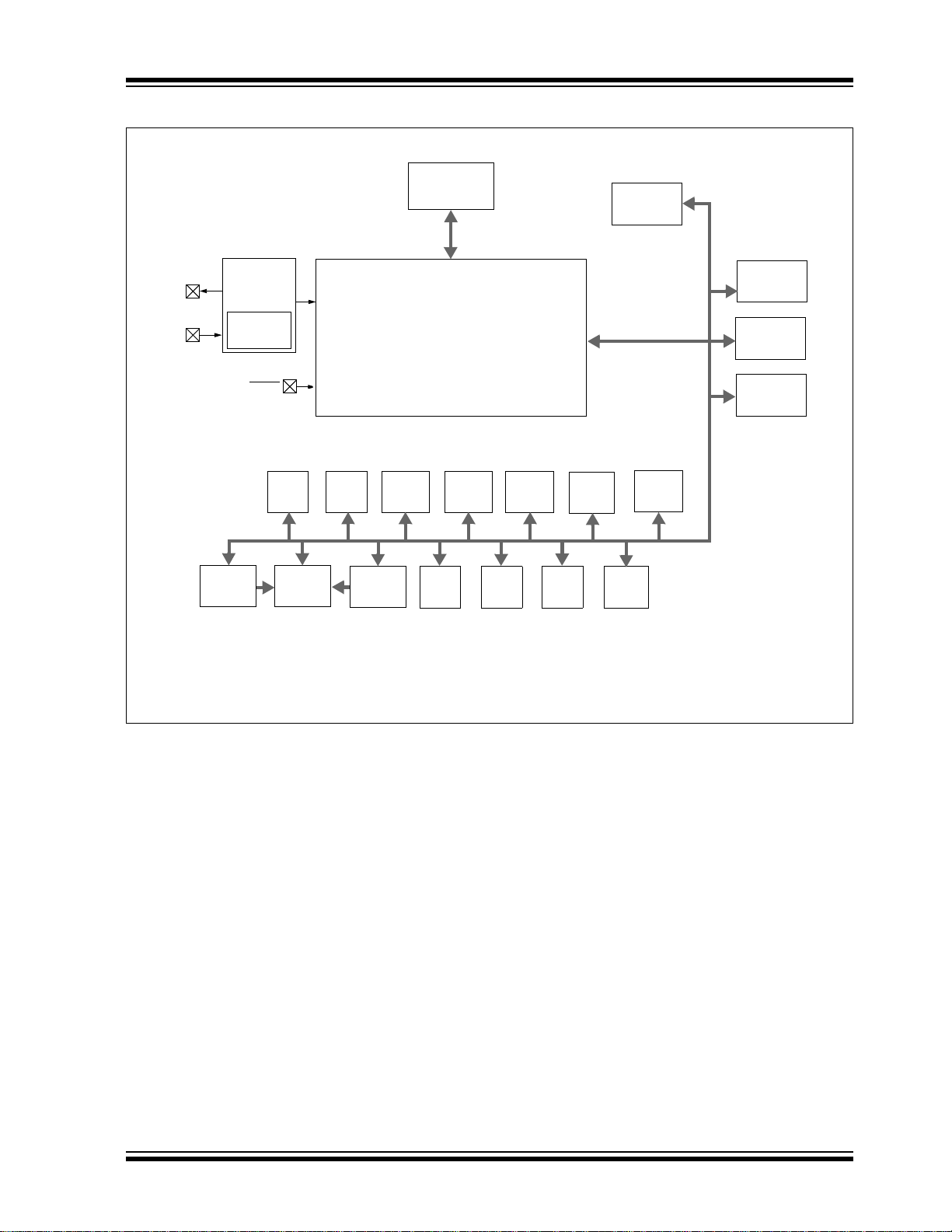
FIGURE 1-1: PIC16(L)F1507 BLOCK DIAGRAM
PORTB
PORTC
Note 1: See applicable chapters for more information on peripherals.
2: See Ta bl e 1 -1 for peripherals available on specific devices.
CPU
Program
Flash Memory
RAM
Timing
Generation
INTRC
Oscillator
MCLR
(Figure 2-1)
NCO1
PWM4
Timer2Timer1Timer0
CLC2
PWM1 PWM2
PWM3
PORTA
CWG1
CLC1
ADC
10-Bit
FVR
Te mp .
Indicator
CLKIN
CLKOUT
PIC16(L)F1507
2011 Microchip Technology Inc. Preliminary DS41586A-page 10
PIC16(L)F1507
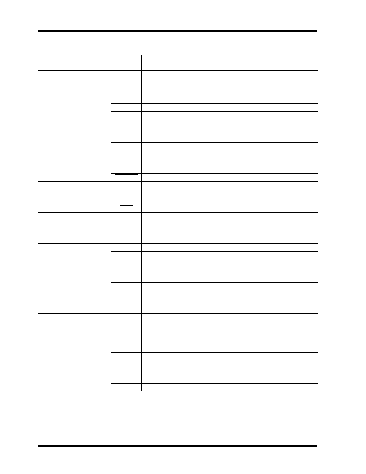
TABLE 1-2: PIC16(L)F1507 PINOUT DESCRIPTION
Input
Name Function
RA0/AN0/ICSPDAT RA0 TTL CMOS General purpose I/O.
AN0 AN — A/D Channel input.
ICSPDAT ST CMOS ICSP™ Data I/O.
RA1/AN1/V
RA2/AN2/T0CKI/INT/PWM3/
CLC1
RA3/CLC1IN0/V
RA4/AN3/CLKOUT/T1G RA4 TTL CMOS General purpose I/O.
RA5/CLKIN/T1CKI/NCO1CLK RA5 TTL CMOS General purpose I/O.
RB4/AN10 RB4 TTL CMOS General purpose I/O.
RB5/AN11 RB5 TTL CMOS General purpose I/O.
RB6 RB6 TTL CMOS General purpose I/O.
RB7 RB7 TTL CMOS General purpose I/O.
RC0/AN4/CLC2 RC0 TTL CMOS General purpose I/O.
RC1/AN5/PWM4/NCO1
RC2/AN6 RC2 TTL CMOS General purpose I/O.
Legend: AN = Analog input or output CMOS = CMOS compatible input or output OD = Open Drain
Note 1: Default location for peripheral pin function. Alternate location can be selected using the APFCON register.
REF+/ICSPCLK RA1 TTL CMOS General purpose I/O.
AN1 AN — A/D Channel input.
REF+ AN — A/D Positive Voltage Reference input.
V
ICSPCLK ST — Serial Programming Clock.
(1)
/CWG1FLT
PP/MCLR RA3 TTL — General purpose input.
(1)
TTL = TTL compatible input ST = Schmitt Trigger input with CMOS levels I
HV = High Voltage XTAL = Crystal levels
2: Alternate location for peripheral pin function selected by the APFCON register.
RA2 ST CMOS General purpose I/O.
AN2 AN — A/D Channel input.
T0CKI ST — Timer0 clock input.
INT ST — External interrupt.
PWM3 — CMOS Pulse Width Module source output.
CLC1 — CMOS Configurable Logic Cell source output.
CWG1FLT
CLC1IN0 ST — Configurable Logic Cell source input.
PP HV — Programming voltage.
V
MCLR
AN3 AN — A/D Channel input.
CLKOUT — CMOS F
T1G ST — Timer1 Gate input.
CLKIN CMOS — External clock input (EC mode).
T1CKI ST — Timer1 clock input.
NCO1CLK ST — Numerically Controlled Oscillator Clock source input.
AN10 AN — A/D Channel input.
AN11 AN — A/D Channel input.
AN4 AN — A/D Channel input.
CLC2 — CMOS Configurable Logic Cell source output.
RC1 TTL CMOS General purpose I/O.
AN5 AN — A/D Channel input.
PWM4 — CMOS Pulse Width Module source output.
NCO1 — CMOS Numerically Controlled Oscillator is source output.
AN6 AN — A/D Channel input.
Output
Type
Type
ST — Complementary Waveform Generator Fault input.
ST — Master Clear with internal pull-up.
OSC/4 output.
Description
2
C™ = Schmitt Trigger input with I2C
DS41586A-page 11 Preliminary 2011 Microchip Technology Inc.
PIC16(L)F1507
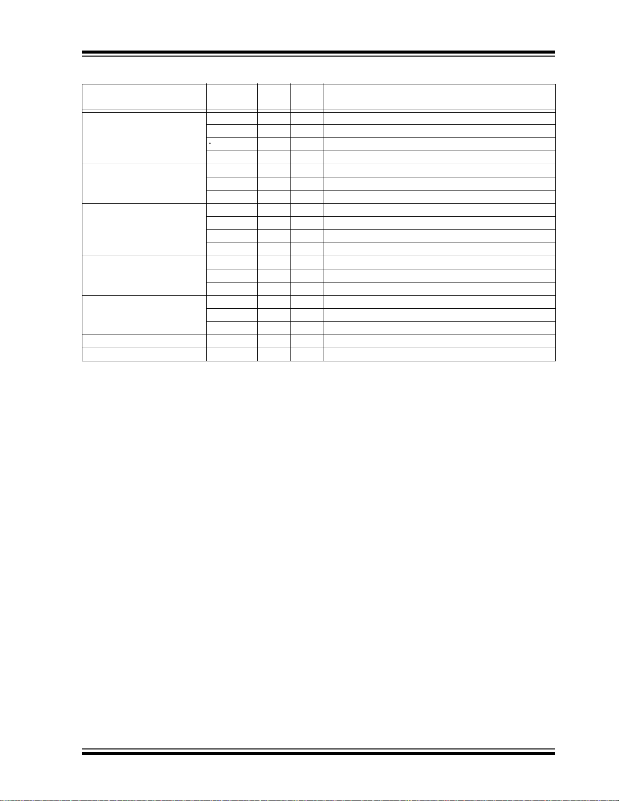
TABLE 1-2: PIC16(L)F1507 PINOUT DESCRIPTION (CONTINUED)
Input
Name Function
RC3/AN7/PWM2/CLC2IN0 RC3 TTL CMOS General purpose I/O.
AN7 AN — A/D Channel input.
PWM2 — CMOS Pulse Width Module source output.
CLC2IN0 ST — Configurable Logic Cell source input.
RC4/CLC2IN1/CWG1B RC4 TTL CMOS General purpose I/O.
CLC2IN1 ST — Configurable Logic Cell source input.
(2)
RC5/PWM1/CLC1
CWG1A
RC6/AN8/NCO1
RC7/AN9/CLC1IN1 RC7 TTL CMOS General purpose I/O.
DD VDD Power — Positive supply.
V
SS VSS Power — Ground reference.
V
Legend: AN = Analog input or output CMOS = CMOS compatible input or output OD = Open Drain
Note 1: Default location for peripheral pin function. Alternate location can be selected using the APFCON register.
TTL = TTL compatible input ST = Schmitt Trigger input with CMOS levels I
HV = High Voltage XTAL = Crystal levels
2: Alternate location for peripheral pin function selected by the APFCON register.
/
(2)
CWG1B — CMOS CWG complementary output.
RC5 TTL CMOS General purpose I/O.
PWM1 — CMOS PWM output.
CLC1 — CMOS Configurable Logic Cell source output.
CWG1A — CMOS CWG primary output.
RC6 TTL CMOS General purpose I/O.
AN8 AN — A/D Channel input.
NCO1 — CMOS Numerically Controlled Oscillator source output.
AN8 AN — A/D Channel input.
CLC1IN1 ST — Configurable Logic Cell source input.
Type
Output
Type
Description
2
C™ = Schmitt Trigger input with I2C
2011 Microchip Technology Inc. Preliminary DS41586A-page 12

PIC16(L)F1507
2.0 ENHANCED MID-RANGE CPU
This family of devices contain an enhanced mid-range
8-bit CPU core. The CPU has 49 instructions. Interrupt
capability includes automatic context saving. The
hardware stack is 16 levels deep and has Overflow and
Underflow Reset capability. Direct, Indirect, and
Relative addressing modes are available. Two File
Select Registers (FSRs) provide the ability to read
program and data memory.
• Automatic Interrupt Context Saving
• 16-level Stack with Overflow and Underflow
• File Select Registers
• Instruction Set
2.1 Automatic Interrupt Context Saving
During interrupts, certain registers are automatically
saved in shadow registers and restored when returning
from the interrupt. This saves stack space and user
code. See Section 7.5 “Automatic Context Saving”,
for more information.
2.2 16-level St ack with Overflow and Underflow
These devices have an external stack memory 15 bits
wide and 16 words deep. A Stack Overflow or Underflow will set the appropriate bit (STKOVF or STKUNF)
in the PCON register, and if enabled will cause a software Reset. See section Section 3.4 “St ack” for more
details.
2.3 File Select Registers
There are two 16-bit File Select Registers (FSR). FSRs
can access all file registers and program memory,
which allows one Data Pointer for all memory. When an
FSR points to program memory, there is one additional
instruction cycle in instructions using INDF to allow the
data to be fetched. General purpose memory can now
also be addressed linearly, providing the ability to
access contiguous data larger than 80 bytes. There are
also new instructions to support the FSRs. See
Section 3.5 “Indirect Addressing” for more details.
2.4 Instruction Set
There are 49 instructions for the enhanced mid-range
CPU to support the features of the CPU. See
Section 24.0 “Instruction Set Summary” for more
details.
DS41586A-page 13 Preliminary 2011 Microchip Technology Inc.
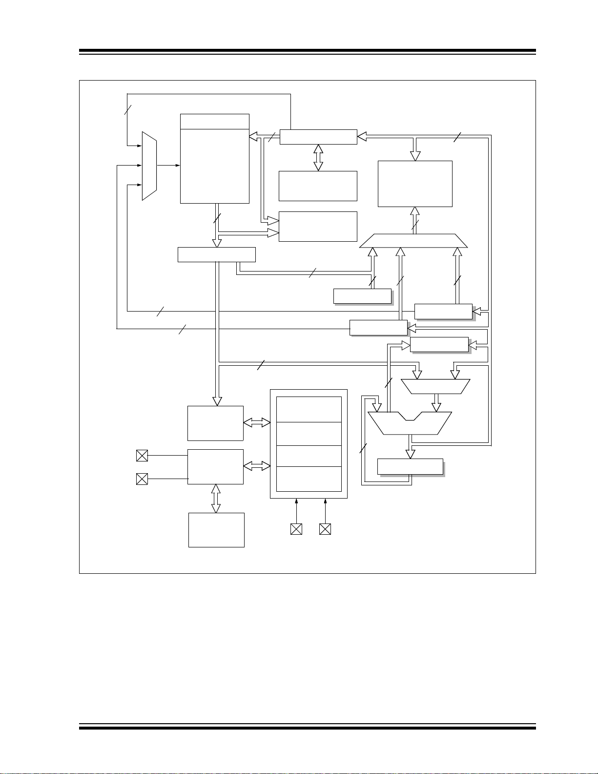
FIGURE 2-1: CORE BLOCK DIAGRAM
Data Bus
8
14
Program
Bus
Instruction reg
Program Counter
8 Level Stack
(13-bit)
Direct Addr
7
12
Addr MUX
FSR reg
STATUS reg
MUX
ALU
Instruction
Decode &
Control
Timing
Generation
CLKIN
CLKOUT
8
8
12
3
Internal
Oscillator
Block
Configuration
Data Bus
8
14
Program
Bus
Instruction reg
Program Counter
8 Level Stack
(13-bit)
Direct Addr
7
Addr MUX
FSR reg
STATUS reg
MUX
ALU
W Reg
Instruction
Decode &
Control
Timing
Generation
8
8
3
Internal
Oscillator
Block
Configuration
15
Data Bus
8
14
Program
Bus
Instruction Reg
Program Counter
16-Level Stack
(15-bit)
Direct Addr
7
RAM Addr
Addr MUX
Indirect
Addr
FSR0 Reg
STATUS Reg
MUX
ALU
Instruction
Decode and
Control
Timing
Generation
8
8
3
Internal
Oscillator
Block
Configuration
Flash
Program
Memory
RAM
FSR regFSR reg
FSR1 Reg
15
15
MUX
15
Program Memory
Read (PMR)
12
FSR regFSR reg
BSR Reg
5
Power-up
Timer
Power-on
Reset
Watchdog
Timer
V
DD
Brown-out
Reset
VSSVDD VSSVDD VSS
PIC16(L)F1507
2011 Microchip Technology Inc. Preliminary DS41586A-page 14

PIC16(L)F1507
3.0 MEMORY ORGANIZATION
These devices contain the following types of memory:
• Program Memory
- Configuration Words
-Device ID
-User ID
- Flash Program Memory
• Data Memory
- Core Registers
- Special Function Registers
- General Purpose RAM
- Common RAM
TABLE 3-1: DEVICE SIZES AND ADDRESSES
Device Program Memory Space (Words) Last Program Memory Address
PIC16F1507
PIC16LF1507
2,048 07FFh
The following features are associated with access and
control of program memory and data memory:
• PCL and PCLATH
•Stack
• Indirect Addressing
3.1 Program Memory Organization
The enhanced mid-range core has a 15-bit program
counter capable of addressing 32K x 14 program
memory space. Table 3-1 shows the memory sizes
implemented. Accessing a location above these
boundaries will cause a wrap-around within the
implemented memory space. The Reset vector is at
0000h and the interrupt vector is at 0004h (See
Figure 3-1).
DS41586A-page 15 Preliminary 2011 Microchip Technology Inc.

PIC16(L)F1507
PC<14:0>
15
0000h
0004h
Stack Level 0
Stack Level 15
Reset Vector
Interrupt Vector
Stack Level 1
0005h
On-chip
Program
Memory
Page 0
07FFh
Wraps to Page 0
Wraps to Page 0
Wraps to Page 0
0800h
CALL, CALLW
RETURN, RETLW
Interrupt, RETFIE
Rollover to Page 0
Rollover to Page 0
7FFFh
constants
BRW ;Add Index in W to
;program counter to
;select data
RETLW DATA0 ;Index0 data
RETLW DATA1 ;Index1 data
RETLW DATA2
RETLW DATA3
my_function
;… LOTS OF CODE…
MOVLW DATA_INDEX
call constants
;… THE CONSTANT IS IN W
FIGURE 3-1: PROGRAM MEMORY MAP
AND STACK FOR
PIC16(L)F1507
3.1.1 READING PROGRAM MEMORY AS DATA
There are two methods of accessing constants in program memory. The first method is to use tables of
RETLW instructions. The second method is to set an
FSR to point to the program memory.
3.1.1.1 RETLW Instruction
The RETLW instruction can be used to provide access
to tables of constants. The recommended way to create
such a table is shown in Example 3-1.
EXAMPLE 3-1: RETLW INSTRUCTION
The BRW instruction makes this type of table very simple to implement. If your code must remain portable
with previous generations of microcontrollers, then the
BRW instruction is not available so the older table read
method must be used.
2011 Microchip Technology Inc. Preliminary DS41586A-page 16

PIC16(L)F1507
constants
RETLW DATA0 ;Index0 data
RETLW DATA1 ;Index1 data
RETLW DATA2
RETLW DATA3
my_function
;… LOTS OF CODE…
MOVLW LOW constants
MOVWF FSR1L
MOVLW HIGH constants
MOVWF FSR1H
MOVIW 0[FSR1]
;THE PROGRAM MEMORY IS IN W
Addresses BANKx
x00h or x80h INDF0
x01h or x81h INDF1
x02h or x82h PCL
x03h or x83h STATUS
x04h or x84h FSR0L
x05h or x85h FSR0H
x06h or x86h FSR1L
x07h or x87h FSR1H
x08h or x88h BSR
x09h or x89h WREG
x0Ah or x8Ah PCLATH
x0Bh or x8Bh INTCON
3.1.1.2 Indirect Read with FSR
The program memory can be accessed as data by setting bit 7 of the FSRxH register and reading the matching INDFx register. The MOVIW instruction will place the
lower 8 bits of the addressed word in the W register.
Writes to the program memory cannot be performed via
the INDF registers. Instructions that access the program memory via the FSR require one extra instruction
cycle to complete. Example 3-2 demonstrates accessing the program memory via an FSR.
The HIGH directive will set bit<7> if a label points to a
location in program memory.
EXAMPLE 3-2: ACCESSING PROGRAM
MEMORY VIA FSR
3.2.1 CORE REGISTERS
The core registers contain the registers that directly
affect the basic operation. The core registers occupy
the first 12 addresses of every data memory bank
(addresses x00h/x08h through x0Bh/x8Bh). These
registers are listed below in Ta bl e 3 -2. For for detailed
information, see Tab le 3 -4 .
TABLE 3-2: CORE REGISTERS
3.2 Data Memory Organization
The data memory is partitioned in 32 memory banks
with 128 bytes in a bank. Each bank consists of
(Figure 3-2):
• 12 core registers
• 20 Special Function Registers (SFR)
• Up to 80 bytes of General Purpose RAM (GPR)
• 16 bytes of common RAM
The active bank is selected by writing the bank number
into the Bank Select Register (BSR). Unimplemented
memory will read as ‘0’. All data memory can be
accessed either directly (via instructions that use the
file registers) or indirectly via the two File Select
Registers (FSR). See Section 3.5 “Indirect
Addressing” for more information.
Data Memory uses a 12-bit address. The upper 7-bit of
the address define the Bank address and the lower
5-bits select the registers/RAM in that bank.
DS41586A-page 17 Preliminary 2011 Microchip Technology Inc.

PIC16(L)F1507
3.2.1.1 STATUS Register
The STATUS register, shown in Register 3-1, contains:
• the arithmetic status of the ALU
• the Reset status
The STATUS register can be the destination for any
instruction, like any other register. If the STATUS
register is the destination for an instruction that affects
the Z, DC or C bits, then the write to these three bits is
disabled. These bits are set or cleared according to the
device logic. Furthermore, the TO
writable. Therefore, the result of an instruction with the
STATUS register as destination may be different than
intended.
and PD bits are not
For example, CLRF STATUS will clear the upper three
bits and set the Z bit. This leaves the STATUS register
as ‘000u u1uu’ (where u = unchanged).
It is recommended, therefore, that only BCF, BSF,
SWAPF and MOVWF instructions are used to alter the
STATUS register, because these instructions do not
affect any Status bits. For other instructions not
affecting any Status bits (Refer to Section 24.0
“Instruction Set Summary”).
Note 1: The C and DC bits operate as Borrow
and Digit Borrow out bits, respectively, in
subtraction.
REGISTER 3-1: STATUS: STATUS REGISTER
U-0 U-0 U-0 R-1/q R-1/q R/W-0/u R/W-0/u R/W-0/u
— — —
bit 7 bit 0
Legend:
R = Readable bit W = Writable bit U = Unimplemented bit, read as ‘0’
u = Bit is unchanged x = Bit is unknown -n/n = Value at POR and BOR/Value at all other Resets
‘1’ = Bit is set ‘0’ = Bit is cleared q = Value depends on condition
TO
PD ZDC
(1)
(1)
C
bit 7-5 Unimplemented: Read as ‘0’
bit 4 TO
bit 3 PD
bit 2 Z: Zero bit
bit 1 DC: Digit Carry/Digit Borrow
bit 0 C: Carry/Borrow
Note 1: For Borrow, the polarity is reversed. A subtraction is executed by adding the two’s complement of the
second operand. For rotate (RRF, RLF) instructions, this bit is loaded with either the high-order or low-order
bit of the source register.
: Time-Out bit
1 = After power-up, CLRWDT instruction or SLEEP instruction
0 = A WDT time-out occurred
: Power-Down bit
1 = After power-up or by the CLRWDT instruction
0 = By execution of the SLEEP instruction
1 = The result of an arithmetic or logic operation is zero
0 = The result of an arithmetic or logic operation is not zero
bit (ADDWF, ADDLW, SUBLW, SUBWF instructions)
1 = A carry-out from the 4th low-order bit of the result occurred
0 = No carry-out from the 4th low-order bit of the result
(1)
bit
(ADDWF, ADDLW, SUBLW, SUBWF instructions)
1 = A carry-out from the Most Significant bit of the result occurred
0 = No carry-out from the Most Significant bit of the result occurred
(1)
(1)
2011 Microchip Technology Inc. Preliminary DS41586A-page 18

PIC16(L)F1507
0Bh
0Ch
1Fh
20h
6Fh
70h
7Fh
00h
Common RAM
(16 bytes)
General Purpose RAM
(80 bytes maximum)
Core Registers
(12 bytes)
Special Function Registers
(20 bytes maximum)
Memory Region
7-bit Bank Offset
3.2.2 SPECIAL FUNCTION REGISTER
The Special Function Registers are registers used by
the application to control the desired operation of
peripheral functions in the device. The Special Function
Registers occupy the 20 bytes after the core registers of
every data memory bank (addresses x0Ch/x8Ch
through x1Fh/x9Fh). The registers associated with the
operation of the peripherals are described in the appropriate peripheral chapter of this data sheet.
3.2.3 GENERAL PURPOSE RAM
There are up to 80 bytes of GPR in each data memory
bank. The Special Function Registers occupy the 20
bytes after the core registers of every data memory
bank (addresses x0Ch/x8Ch through x1Fh/x9Fh).
3.2.3.1 Linear Access to GPR
The general purpose RAM can be accessed in a
non-banked method via the FSRs. This can simplify
access to large memory structures. See Section 3.5.2
“Linear Data Memory” for more information.
3.2.4 COMMON RAM
There are 16 bytes of common RAM accessible from all
banks.
FIGURE 3-2: BANKED MEMORY
PARTITIONING
DS41586A-page 19 Preliminary 2011 Microchip Technology Inc.
3.2.5 DEVICE MEMORY MAPS
The memory maps for PIC16(L)F1507 are as shown in
Table 3-3.

DS41586A-page 20 Preliminary 2011 Microchip Technology Inc.
TABLE 3-3: PIC16(L)F1507 MEMORY MAP
PIC16(L)F1507
BANK 0 BANK 1 BANK 2 BANK 3 BANK 4 BANK 5 BANK 6 BANK 7
000h
Core Registers
(Ta bl e 3 - 2)
00Bh 08Bh 10Bh 18Bh 20Bh 28Bh 30Bh 38Bh
00Ch PORTA 08Ch TRISA 10Ch LATA 18Ch ANSELA 20Ch WPUA 28Ch
00Dh PORTB 08Dh TRISB 10Dh LATB 18Dh ANSELB 20Dh WPUB 28Dh
00Eh PORTC 08Eh TRISC 10Eh LATC 18Eh ANSELC 20Eh
00Fh
010h
011h PIR1 091h PIE1 111h
012h PIR2 092h PIE2 112h
013h PIR3 093h PIE3 113h
014h
015h TMR0 095h OPTION_REG 115h
016h
017h
018h
019h
01Ah
01Bh
01Ch
01Dh
01Eh
01Fh
020h
06Fh
070h
07Fh 0FFh 17Fh 1FFh 27Fh 2FFh 37Fh 3FFh
Legend: = Unimplemented data memory locations, read as ‘0’
—08Fh—10Fh—18Fh—20Fh—28Fh—30Fh—38Fh—
—090h—110h—190h—210h—290h
—094h—114h
TMR1L 096h PCON 116h BORCON 196h PMCON2 216h
TMR1H 097h WDTCON 117h FVRCON 197h VREGCON 217h
T1CON 098h
T1GCON 099h OSCCON 119h
TMR2 09Ah OSCSTAT 11Ah
PR2 09BhADRESL11Bh
T2CON 09Ch ADRESH 11Ch
— 09Dh ADCON0 11Dh APFCON 19Dh
—
—
General
Purpose
Register
80 Bytes
Common RAM
080h
Core Registers
(Ta bl e 3 - 2)
—118h—198h—218h
09Eh ADCON1 11Eh
09Fh ADCON2 11Fh
0A0h
0BFh
0C0h
0EFh
0F0h
General
Purpose
Register
32 Bytes
Unimplemented
Read as ‘0’
Common RAM
(Accesses
70h – 7Fh)
100h
120h
16Fh 1EFh 26Fh 2EFh
170h
Core Registers
(Table 3-2)
—
—
—
—
—
—199h
—19Ah
—19Bh
— 19Ch
—
—19Fh
Unimplemented
Read as ‘0’
Common RAM
(Accesses
70h – 7Fh)
180h
Core Registers
(Table 3-2)
191h PMADRL 211h
192h PMADRH 212h
193h PMDATL 213h
194h PMDATH 214h
195h PMCON1 215h
—
—
—
—
—
19Eh
1A0h
1F0h
—
—
Unimplemented
Read as ‘0’
Common RAM
(Accesses
70h – 7Fh)
200h
219h
21Ah
21Bh
21Ch
21Dh
21Eh
21Fh
220h
270h
Core Registers
(Table 3-2)
—28Eh—30Eh—38Eh—
—
—
—
—
—
—
—
—
—299h— 319h — 399h —
—29Ah—31Ah—39Ah—
—29Bh—31Bh
— 29Ch — 31Ch
—
—
—
Unimplemented
Read as ‘0’
Common RAM
(Accesses
70h – 7Fh)
280h
291h
292h
293h
294h
295h
296h
297h
298h
29Dh
29Eh
29Fh
2A0h
2F0h
Core Registers
(Table 3-2)
— 30Ch — 38Ch —
— 30Dh — 38Dh —
—
—
—
—
—
—
— 316h — 396h IOCBF
— 317h — 397h —
— 318h — 398h —
—
—
—
Unimplemented
Read as ‘0’
Common RAM
(Accesses
70h – 7Fh)
300h
Core Registers
(Table 3-2)
310h
311h
312h
313h
314h
315h
31Dh
31Eh
31Fh
320h
36Fh 3EFh
370h
— 390h —
—
—
—
—
—
—
—
—
—
—
Unimplemented
Read as ‘0’
Common RAM
(Accesses
70h – 7Fh)
380h
391h IOCAP
392h IOCAN
393h
394h IOCBP
395h IOCBN
39Bh
39Ch
39Dh
39Eh
39Fh
3A0h
3F0h
Core Registers
(Table 3-2)
IOCAF
—
—
—
—
—
Unimplemented
Read as ‘0’
Common RAM
(Accesses
70h – 7Fh)

2011 Microchip Technology Inc. Preliminary DS41586A-page 21
TABLE 3-3: PIC16(L)F1507 MEMORY MAP (CONTINUED)
BANK 8 BANK 9 BANK 10 BANK 11 BANK 12 BANK 13 BANK 14 BANK 15
400h
40Bh
40Ch
40Dh
40Eh
40Fh
410h
411h
412h
413h
414h
415h
416h
417h
418h
419h
41Ah
41Bh
41Ch
41Dh
41Eh
41Fh
420h
Core Registers
(Ta bl e 3 - 2)
— 48Ch — 50Ch — 58Ch — 60Ch — 68Ch — 70Ch — 78Ch —
— 48Dh — 50Dh — 58Dh — 60Dh — 68Dh — 70Dh — 78Dh —
—48Eh—50Eh—58Eh—60Eh—68Eh—70Eh—78Eh—
—48Fh—50Fh—58Fh—60Fh—68Fh—70Fh—78Fh—
—490h—510h—590h—610h—690h— 710h — 790h —
—491h—511h—591h— 611h PWM1DCL 691h CWG1DBR 711h — 791h —
—492h—512h—592h— 612h PWM1DCH 692h CWG1DBF 712h — 792h —
—493h—513h—593h— 613h PWM1CON 693h CWG1CON0 713h — 793h —
—494h—514h—594h— 614h PWM2DCL 694h CWG1CON1 714h — 794h —
—495h—515h—595h— 615h PWM2DCH 695h CWG1CON2 715h — 795h —
—496h—516h—596h— 616h PWM2CON 696h — 716h — 796h —
—497h—517h—597h— 617h PWM3DCL 697h — 717h — 797h —
— 498h NCO1ACCL 518h —598h— 618h PWM3DCH 698h — 718h — 798h —
— 499h NCO1ACCH 519h —599h— 619h PWM3CON 699h — 719h — 799h —
— 49Ah NCO1ACCU 51Ah —59Ah— 61Ah PWM4DCL 69Ah —71Ah—79Ah—
— 49Bh NCO1INCL 51Bh —59Bh— 61Bh PWM4DCH 69Bh —71Bh—79Bh—
— 49Ch NCO1INCH 51Ch — 59Ch — 61Ch PWM4CON 69Ch — 71Ch — 79Ch —
— 49Dh — 51Dh — 59Dh — 61Dh — 69Dh — 71Dh — 79Dh —
— 49Eh NCO1CON 51Eh —59Eh—61Eh—69Eh—71Eh—79Eh—
— 49Fh NCO1CLK 51Fh —59Fh—61Fh—69Fh—71Fh—79Fh—
480h
48Bh
4A0h
Core Registers
(Ta bl e 3 - 2)
500h
50Bh
520h
Core Registers
(Table 3-2)
580h
Core Registers
58Bh
5A0h
(Table 3-2)
600h
60Bh
620h
Core Registers
(Table 3-2)
680h
68Bh
6A0h
Core Registers
(Table 3-2)
700h
70Bh
720h
Core Registers
(Table 3-2)
780h
78Bh
7A0h
Core Registers
(Table 3-2)
Unimplemented
Read as ‘0’
46Fh 4EFh 56Fh 5EFh 64Fh 6EFh 76Fh 7EFh
470h
Common RAM
(Accesses
47Fh 4FFh 57Fh 5FFh 67Fh 6FFh 77Fh 7FFh
70h – 7Fh)
4F0h
Unimplemented
Read as ‘0’
Common RAM
(Accesses
70h – 7Fh)
570h
Unimplemented
Read as ‘0’
Common RAM
(Accesses
70h – 7Fh)
5F0h
Unimplemented
Read as ‘0’
Common RAM
(Accesses
70h – 7Fh)
650h
Unimplemented
Read as ‘0’
Common RAM
(Accesses
70h – 7Fh)
6F0h
Unimplemented
Read as ‘0’
Common RAM
(Accesses
70h – 7Fh)
770h
Unimplemented
Read as ‘0’
Common RAM
(Accesses
70h – 7Fh)
7F0h
BANK 16 BANK 17 BANK 18 BANK 19 BANK 20 BANK 21 BANK 22 BANK 23
800h
Core Registers
(Ta bl e 3 - 2)
80Bh
80Ch
Unimplemented
Read as ‘0’
86Fh 8EFh 96Fh
870h
Common RAM
(Accesses
87Fh 8FFh 97Fh 9FFh A7Fh AFFh B7Fh BFFh
Legend: = Unimplemented data memory locations, read as ‘0’
70h – 7Fh)
880h
88Bh
88Ch
8F0h
Core Registers
(Ta bl e 3 - 2)
Unimplemented
Read as ‘0’
Common RAM
(Accesses
70h – 7Fh)
900h
90Bh
90Ch
970h
Core Registers
(Table 3-2)
Unimplemented
Read as ‘0’
Common RAM
(Accesses
70h – 7Fh)
980h
98Bh
98Ch
9EFh
9F0h
Core Registers
(Table 3-2)
Unimplemented
Read as ‘0’
Common RAM
(Accesses
70h – 7Fh)
A00h
A0Bh
A0Ch
A6Fh
A70h
Core Registers
(Table 3-2)
Unimplemented
Read as ‘0’
Common RAM
(Accesses
70h – 7Fh)
A80h
A8Bh
A8Ch
AEFh
AF0h
Core Registers
(Table 3-2)
Unimplemented
Read as ‘0’
Common RAM
(Accesses
70h – 7Fh)
B00h
B0Bh
B0Ch
B6Fh
B70h
Core Registers
(Table 3-2)
Unimplemented
Read as ‘0’
Common RAM
(Accesses
70h – 7Fh)
B80h
B8Bh
B8Ch
BEFh
BF0h
Unimplemented
Read as ‘0’
Common RAM
(Accesses
70h – 7Fh)
Core Registers
(Table 3-2)
Unimplemented
Read as ‘0’
Common RAM
(Accesses
70h – 7Fh)
PIC16(L)F1507

DS41586A-page 22 Preliminary 2011 Microchip Technology Inc.
Legend: = Unimplemented data memory locations, read as ‘0’.
BANK 24 BANK 25 BANK 26 BANK 27 BANK 28 BANK 29 BANK 30 BANK 31
C00h
C0Bh
Core Registers
(Ta bl e 3 -2 )
C80h
C8Bh
Core Registers
(Ta bl e 3 -2 )
D00h
D0Bh
Core Registers
(Ta bl e 3 -2 )
D80h
D8Bh
Core Registers
(Ta bl e 3 -2 )
E00h
E0Bh
Core Registers
(Ta bl e 3 -2 )
E80h
E8Bh
Core Registers
(Ta bl e 3 -2 )
F00h
F0Bh
Core Registers
(Ta bl e 3 -2 )
F80h
F8Bh
Core Registers
(Ta bl e 3 -2 )
C0Ch
—C8Ch—D0Ch—D8Ch—E0Ch—E8Ch—F0Ch
See Tab l e 3 -3 for
register mapping
details
F8Ch
See Tab l e 3 -3 for
register mapping
details
C0Dh
—C8Dh—D0Dh—D8Dh—E0Dh—E8Dh— F0Dh F8Dh
C0Eh
—C8Eh—D0Eh—D8Eh—E0Eh—E8Eh— F0Eh F8Eh
C0Fh
—C8Fh—D0Fh—D8Fh—E0Fh—E8Fh— F0Fh F8Fh
C10h
—C90h—D10h—D90h—E10h—E90h— F10h F90h
C11h
—C91h—D11h—D91h—E11h—E91h— F11h F91h
C12h
—C92h—D12h—D92h—E12h—E92h— F12h F92h
C13h
—C93h—D13h—D93h—E13h—E93h— F13h F93h
C14h
—C94h—D14h—D94h—E14h—E94h— F14h F94h
C15h
—C95h—D15h—D95h—E15h—E95h— F15h F95h
C16h
—C96h—D16h—D96h—E16h—E96h— F16h F96h
C17h
—C97h—D17h—D97h—E17h—E97h— F17h F97h
C18h
—C98h—D18h—D98h—E18h—E98h— F18h F98h
C19h
—C99h—D19h—D99h—E19h—E99h— F19h F99h
C1Ah
—C9Ah—D1Ah—D9Ah—E1Ah—E9Ah— F1Ah F9Ah
C1Bh
—C9Bh—D1Bh—D9Bh—E1Bh—E9Bh— F1Bh F9Bh
C1Ch
—C9Ch—D1Ch—D9Ch—E1Ch—E9Ch— F1Ch F9Ch
C1Dh
—C9Dh—D1Dh—D9Dh—E1Dh—E9Dh— F1Dh F9Dh
C1Eh
—C9Eh—D1Eh—D9Eh—E1Eh—E9Eh— F1Eh F9Eh
C1Fh
—C9Fh—D1Fh—D9Fh—E1Fh—E9Fh— F1Fh F9Fh
C20h
Unimplemented
Read as ‘0’
CA0h
Unimplemented
Read as ‘0’
D20h
Unimplemented
Read as ‘0’
DA0h
Unimplemented
Read as ‘0’
E20h
Unimplemented
Read as ‘0’
EA0h
Unimplemented
Read as ‘0’
F20h FA0h
C6Fh CEFh D6Fh DEFh E6Fh EEFh F6Fh FEFh
C70h
Common RAM
(Accesses
70h – 7Fh)
CF0h
Common RAM
(Accesses
70h – 7Fh)
D70h
Common RAM
(Accesses
70h – 7Fh)
DF0h
Common RAM
(Accesses
70h – 7Fh)
E70h
Common RAM
(Accesses
70h – 7Fh)
EF0h
Common RAM
(Accesses
70h – 7Fh)
F70h
Common RAM
(Accesses
70h – 7Fh)
FF0h
Common RAM
(Accesses
70h – 7Fh)
CFFh
CFFh D7Fh DFFh E7Fh EFFh F7Fh FFFh
TABLE 3-3: PIC16(L)F1507 MEMORY MAP (CONTINUED)
PIC16(L)F1507

PIC16(L)F1507
Bank 30
F0Ch
—
F0Dh
—
F0Eh
—
F0Fh
CLCDATA
F10h
CLC1CON
F11h
CLC1POL
F12h
CLC1SEL0
F13h
CLC1SEL1
F14h
CLC1GLS0
F15h
CLC1GLS1
F16h
CLC1GLS2
F17h
CLC1GLS3
F18h
CLC2CON
F19h
CLC2POL
F1Ah
CLC2SEL0
F1Bh
CLC2SEL1
F1Ch
CLC2GLS0
F1Dh
CLC2GLS1
F1Eh
CLC2GLS2
F1Fh
CLC2GLS3
F20h
Unimplemented
Read as ‘0’
F6Fh
Bank 31
F8Ch
FE3h
Unimplemented
Read as ‘0’
FE4h
STATUS_SHAD
FE5h
WREG_SHAD
FE6h
BSR_SHAD
FE7h
PCLATH_SHAD
FE8h
FSR0L_SHAD
FE9h
FSR0H_SHAD
FEAh
FSR1L_SHAD
FEBh
FSR1H_SHAD
FECh
—
FEDh
STKPTR
FEEh
TOSL
FEFh
TOSH
Legend: = Unimplemented data memory locations, read as ‘0’.
TABLE 3-3: PIC16(L)F1507 MEMORY MAP (CONTINUED)
DS41586A-page 23 Preliminary 2011 Microchip Technology Inc.

PIC16(L)F1507
3.2.6 CORE FUNCTION REGISTERS SUMMARY
The Core Function registers listed in Ta bl e 3 - 4 can be
addressed from any Bank.
TABLE 3-4: CORE FUNCTION REGISTERS SUMMARY
Addr Name Bit 7 Bit 6 Bit 5 Bit 4 Bit 3 Bit 2 Bit 1 Bit 0
Bank 0-31
x00h or
INDF0
x80h
x01h or
INDF1
x81h
x02h or
PCL Program Counter (PC) Least Significant Byte 0000 0000 0000 0000
x82h
x03h or
STATUS
x83h
x04h or
FSR0L Indirect Data Memory Address 0 Low Pointer 0000 0000 uuuu uuuu
x84h
x05h or
FSR0H Indirect Data Memory Address 0 High Pointer 0000 0000 0000 0000
x85h
x06h or
FSR1L Indirect Data Memory Address 1 Low Pointer 0000 0000 uuuu uuuu
x86h
x07h or
FSR1H Indirect Data Memory Address 1 High Pointer 0000 0000 0000 0000
x87h
x08h or
BSR
x88h
x09h or
WREG Working Register 0000 0000 uuuu uuuu
x89h
x0Ah or
PCLATH
x8Ah
x0Bh or
INTCON GIE PEIE TMR0IE INTE IOCIE TMR0IF INTF IOCIF 0000 0000 0000 0000
x8Bh
Legend: x = unknown, u = unchanged, q = value depends on condition, - = unimplemented, read as ‘0’, r = reserved.
Addressing this location uses contents of FSR0H/FSR0L to address data memory
(not a physical register)
Addressing this location uses contents of FSR1H/FSR1L to address data memory
(not a physical register)
— — —TOPD ZDCC---1 1000 ---q quuu
— — —BSR<4:0>---0 0000 ---0 0000
— Write Buffer for the upper 7 bits of the Program Counter -000 0000 -000 0000
Shaded locations are unimplemented, read as ‘0’.
Value on
POR, BOR
xxxx xxxx uuuu uuuu
xxxx xxxx uuuu uuuu
Value on all
other resets
2011 Microchip Technology Inc. Preliminary DS41586A-page 24

PIC16(L)F1507
TABLE 3-5: SPECIAL FUNCTION REGISTER SUMMARY
Address Name Bit 7 Bit 6 Bit 5 B it 4 Bit 3 Bit 2 Bit 1 Bit 0
Value on
POR, BOR
Bank 0
00Ch PORTA — — RA5 RA4 RA3 RA2 RA1 RA0 --xx xxxx --xx xxxx
00Dh PORTB RB7 RB6 RB5 RB4
00Eh PORTC RC7 RC6 RC5 RC4 RC3 RC2 RC1 RC0 xxxx xxxx xxxx xxxx
00Fh
010h
011h PIR1 TMR1GIF ADIF
012h PIR2
013h PIR3
014h
015h TMR0 Holding Register for the 8-bit Timer0 Count xxxx xxxx uuuu uuuu
016h TMR1L Holding Register for the Least Significant Byte of the 16-bit TMR1 Count xxxx xxxx uuuu uuuu
017h TMR1H Holding Register for the Most Significant Byte of the 16-bit TMR1 Count xxxx xxxx uuuu uuuu
018h T1CON TMR1CS<1:0> T1CKPS<1:0>
019h T1GCON TMR1GE T1GPOL T1GTM T1GSPM T1GGO/
01Ah TMR2 Timer2 Module Register 0000 0000 0000 0000
01Bh PR2 Timer2 Period Register 1111 1111 1111 1111
01Ch T2CON
01Dh
01Eh
01Fh
— Unimplemented — —
— Unimplemented — —
— — — — TMR2IF TMR1IF 00-- --00 00-- --00
— — — — — NCO1IF — — ---- -0-- ---- -0--
— — — — — — CLC2IF CLC1IF ---- --00 ---- --00
— Unimplemented — —
— T2OUTPS<3:0> TMR2ON T2CKPS<1:0> -000 0000 -000 0000
— Unimplemented — —
— Unimplemented — —
— Unimplemented — —
— — — — xxxx ---- xxxx ----
— T1SYNC —TMR1ON0000 -0-0 uuuu -u-u
DONE
T1GVAL —T1GSS0000 0x-0 uuuu ux-u
Bank 1
08Ch TRISA — — TRISA5 TRISA4 —
08Dh TRISB TRISB7 TRISB6 TRISB5 TRISB4
08Eh TRISC TRISC7 TRISC6 TRISC5 TRISC4 TRISC3 TRISC2 TRISC1 TRISC0 1111 1111 1111 1111
08Fh
090h
091h PIE1 TMR1GIE ADIE
092h PIE2
093h PIE3
094h
095h
096h PCON STKOVF STKUNF
097h WDTCON
098h
099h OSCCON
09Ah OSCSTAT
09Bh ADRESL A/D Result Register Low xxxx xxxx uuuu uuuu
09Ch ADRESH A/D Result Register High xxxx xxxx uuuu uuuu
09Dh ADCON0
09Eh ADCON1 ADFM ADCS<2:0>
09Fh ADCON2 TRIGSEL<3:0>
Legend: x = unknown, u = unchanged, q = value depends on condition, - = unimplemented, r = reserved.
Note 1: PIC16F1507 only.
— Unimplemented — —
— Unimplemented — —
— — — — TMR2IE TMR1IE 00-- --00 00-- --00
— — — — —NCO1IE — — ---- -0-- ---- -0--
— — — — — — CLC2IE CLC1IE ---- --00 ---- --00
— Unimplemented — —
OPTION_REG
— Unimplemented — —
Shaded locations are unimplemented, read as ‘0’.
2: Unimplemented, read as ‘1’.
WPUEN INTEDG TMR0CS TMR0SE PSA PS<2:0> 1111 1111 1111 1111
—RWDT RMCLR RI POR BOR 00-1 11qq qq-q qquu
— — WDTPS<4:0> SWDTEN --01 0110 --01 0110
— IRCF<3:0> —SCS<1:0>-011 1-00 -011 1-00
— — —HFIOFR— — LFIOFR HFIOFS 1-q0 --00 q-qq --qq
— CHS<4:0>
(2)
TRISA2 TRISA1 TRISA0 --11 1111 --11 1111
— — — — 1111 ---- 1111 ----
GO/DONE
— —
— — — — 0000 ---- 0000 ----
ADPREF<1:0>
ADON -000 0000 -000 0000
0000 --00 0000 --00
Value on all
other
Resets
DS41586A-page 25 Preliminary 2011 Microchip Technology Inc.
PIC16(L)F1507
TABLE 3-5: SPECIAL FUNCTION REGISTER SUMMARY (CONTINUED)
Address Name Bit 7 Bit 6 Bit 5 Bit 4 Bit 3 Bit 2 Bit 1 Bit 0
Value on
POR, BOR
Bank 2
10Ch LATA — —LATA5LATA4— L ATA2 L ATA1 L ATA0 --xx -xxx --uu -uuu
10Dh LATB LATB7 LATB6 LATB5 LATB4
10Eh LATC LATC7 LATC6 LATC5 LATC4 LATC3 LATC2 LATC1 LATC0 xxxx xxxx uuuu uuuu
10Fh
to
— Unimplemented — —
115 h
116h BORCON SBOREN BORFS
117h FVRCON FVREN FVRRDY TSEN TSRNG
118 h
to
— Unimplemented — —
11C h
11Dh APFCON
11Eh
11Fh
— Unimplemented — —
— Unimplemented — —
— — — — — — CLC1SEL NCO1SEL ---- --00 ---- --00
— — — — — BORRDY 10-- ---q uu-- ---u
— — — — xxxx ---- uuuu ----
— —ADFVR<1:0>0q00 --00 0q00 --00
Bank 3
18Ch ANSELA — — — ANSA4 — ANSA2 ANSA1 ANSA0 ---1 -111 ---1 -111
18Dh ANSELB
18Eh ANSELC ANSC7 ANSC6
18Fh
190h
191h PMADRL Flash Program Memory Address Register Low Byte 0000 0000 0000 0000
192h PMADRH
193h PMDATL Flash Program Memory Read Data Register Low Byte xxxx xxxx uuuu uuuu
194h PMDATH
195h PMCON1
196h PMCON2 Flash Program Memory Control Register 2 0000 0000 0000 0000
197h VREGCON
— Unimplemented — —
— Unimplemented — —
198h
to
— Unimplemented — —
19Fh
— — ANSB5 ANSB4 — — — — --11 ---- --11 ----
— — ANSC3 ANSC2 ANSC1 ANSC0 11-- 1111 11-- 1111
— Flash Program Memory Address Register High Byte -000 0000 -000 0000
— — Flash Program Memory Read Data Register High Byte --xx xxxx --uu uuuu
(2)
—
(1)
——————VREGPMReserved ---- --01 ---- --01
CFGS LWLO FREE WRERR WREN WR RD 0000 x000 0000 q000
Bank 4
20Ch WPUA — — WPUA5 WPUA4 WPUA3 WPUA2 WPUA1 WPUA0 --11 1111 --11 1111
20Dh WPUB WPUB7 WPUB6 WPUB5 WPUB4
20Eh
to
— Unimplemented — —
21Fh
— — — — 1111 ---- 1111 ----
Bank 5
28Ch
— Unimplemented — —
to
29Fh
Bank 6
30Ch
to
— Unimplemented — —
31Fh
Legend: x = unknown, u = unchanged, q = value depends on condition, - = unimplemented, r = reserved.
Note 1: PIC16F1507 only.
Shaded locations are unimplemented, read as ‘0’.
2: Unimplemented, read as ‘1’.
Value on all
other
Resets
2011 Microchip Technology Inc. Preliminary DS41586A-page 26
PIC16(L)F1507
TABLE 3-5: SPECIAL FUNCTION REGISTER SUMMARY (CONTINUED)
Address Name Bit 7 Bit 6 Bit 5 B it 4 Bit 3 Bit 2 Bit 1 Bit 0
Bank 7
38Ch
— Unimplemented — —
to
390h
391h IOCAP
392h IOCAN
393h IOCAF
394h IOCBP IOCBP7 IOCBP6 IOCBP5 IOCBP4
395h IOCBN IOCBN7 IOCBN6 IOCBN5 IOCBN4
396h IOCBF IOCBF7 IOCBF6 IOCBF5 IOCBF4
397h
to
— Unimplemented — —
39Fh
— — IOCAP5 IOCAP4 IOCAP3
— — IOCAN5 IOCAN4 IOCAN3
— — IOCAF5 IOCAF4 IOCAF3
— — — — 0000 ---- 0000 ----
— — — — 0000 ---- 0000 ----
— — — — 0000 ---- 0000 ----
IOCAP2 IOCAP1 IOCAP0
IOCAN2 IOCAN1 IOCAN0
IOCAF2 IOCAF1 IOCAF0
Value on
POR, BOR
--00 0000 --00 0000
--00 0000 --00 0000
--00 0000 --00 0000
Bank 8
40Ch
— Unimplemented — —
to
41Fh
Bank 9
48Ch
to
— Unimplemented — —
497h
498h NCO1ACCL NCO1ACC<7:0> 0000 0000 0000 0000
499h NCO1ACCH NCO1ACC<15:8> 0000 0000 0000 0000
49Ah NCO1ACCU NCO1ACC<23:16> 0000 0000 0000 0000
49Bh NCO1INCL NCO1INC<7:0> 0000 0000 0000 0000
49Ch NCO1INCH NCO1INC<15:8> 0000 0000 0000 0000
49Dh
49Eh NCO1CON N1EN N1OE N1OUT N1POL
49Fh NCO1CLK N1PWS<2:0>
— Unimplemented — —
— — —N1PFM0000 ---0 0000 ---0
— — —N1CKS<1:0>0000 --00 0000 --00
Bank 10
50Ch
— Unimplemented — —
to
51Fh
Bank 11
58Ch
to
— Unimplemented — —
59Fh
Legend: x = unknown, u = unchanged, q = value depends on condition, - = unimplemented, r = reserved.
Note 1: PIC16F1507 only.
Shaded locations are unimplemented, read as ‘0’.
2: Unimplemented, read as ‘1’.
Value on all
other
Resets
DS41586A-page 27 Preliminary 2011 Microchip Technology Inc.
PIC16(L)F1507
TABLE 3-5: SPECIAL FUNCTION REGISTER SUMMARY (CONTINUED)
Address Name Bit 7 Bit 6 Bit 5 Bit 4 Bit 3 Bit 2 Bit 1 Bit 0
Bank 12
60Ch
— Unimplemented — —
to
610h
611h PWM1DCL PWM1DCL<7:6>
612h PWM1DCH PWM1DCH<7:0> xxxx xxxx uuuu uuuu
613h PWM1CON0 PWM1EN PWM1OE PWM1OUT PWM1POL
614h PWM2DCL PWM2DCL<7:6>
615h PWM2DCH PWM2DCH<7:0> xxxx xxxx uuuu uuuu
616h PWM2CON0 PWM2EN PWM2OE PWM2OUT PWM2POL
617h PWM3DCL PWM3DCL<7:6>
618h PWM3DCH PWM3DCH<7:0> xxxx xxxx uuuu uuuu
619h PWM3CON0 PWM3EN PWM3OE PWM3OUT PWM3POL
61Ah PWM4DCL PWM4DCL<7:6>
61Bh PWM4DCH PWM4DCH<7:0> xxxx xxxx uuuu uuuu
61Ch PWM4CON0 PWM4EN PWM4OE PWM4OUT PWM4POL
61Dh
to
— Unimplemented — —
61Fh
— — — — — — 00-- ---- 00-- ----
— — — — 0000 ---- 0000 ----
— — — — — — 00-- ---- 00-- ----
— — — — 0000 ---- 0000 ----
— — — — — — 00-- ---- 00-- ----
— — — — 0000 ---- 0000 ----
— — — — — — 00-- ---- 00-- ----
— — — — 0000 ---- 0000 ----
Value on
POR, BOR
Bank 13
68Ch
— Unimplemented — —
to
690h
691h CWG1DBR
692h CWG1DBF
693h CWG1CON0 G1EN G1OEB G1OEA G1POLB G1POLA
694h CWG1CON1 G1ASDLB<1:0> G1ASDLA<1:0>
695h CWG1ASD G1ASE G1ARSEN
696h
to
— Unimplemented — —
69Fh
Legend: x = unknown, u = unchanged, q = value depends on condition, - = unimplemented, r = reserved.
Note 1: PIC16F1507 only.
Shaded locations are unimplemented, read as ‘0’.
2: Unimplemented, read as ‘1’.
— —CWG1DBR<5:0>--00 0000 --00 0000
— —CWG1DBF<5:0>--xx xxxx --xx xxxx
— —G1CS00000 0--0 0000 0--0
— G1IS<2:0> 0000 -000 0000 -000
— — — — G1ASDSFLT G1ASDSCLC2 00-- --00 00-- --00
Value on all
other
Resets
2011 Microchip Technology Inc. Preliminary DS41586A-page 28
PIC16(L)F1507
TABLE 3-5: SPECIAL FUNCTION REGISTER SUMMARY (CONTINUED)
Address Name Bit 7 Bit 6 Bit 5 B it 4 Bit 3 Bit 2 Bit 1 Bit 0
Value on
POR, BOR
Banks 14-29
x0Ch/
x8Ch
—
x1Fh/
x9Fh
— Unimplemented — —
Bank 30
F0Ch
— Unimplemented — —
to
F0Eh
F0Fh CLCDATA
F10h CLC1CON LC1EN LC1OE LC1OUT LC1INTP LC1INTN LC1MODE<2:0> 0000 0000 0000 0000
F11h CLC1POL LC1POL
F12h CLC1SEL0
F13h CLC1SEL1
F14h CLC1GLS0 LC1G1D4T LC1G1D4N LC1G1D3T LC1G1D3N LC1G1D2T LC1G1D2N LC1G1D1T LC1G1D1N xxxx xxxx uuuu uuuu
F15h CLC1GLS1 LC1G2D4T LC1G2D4N LC1G2D3T LC1G2D3N LC1G2D2T LC1G2D2N LC1G2D1T LC1G2D1N xxxx xxxx uuuu uuuu
F16h CLC1GLS2 LC1G3D4T LC1G3D4N LC1G3D3T LC1G3D3N LC1G3D2T LC1G3D2N LC1G3D1T LC1G3D1N xxxx xxxx uuuu uuuu
F17h CLC1GLS3 LC1G4D4T LC1G4D4N LC1G4D3T LC1G4D3N LC1G4D2T LC1G4D2N LC1G4D1T LC1G4D1N xxxx xxxx uuuu uuuu
F18h CLC2CON LC2EN LC2OE LC2OUT LC2INTP LC2INTN LC2MODE<2:0> 0000 0000 0000 0000
F19h CLC2POL LC2POL
F1Ah CLC2SEL0
F1Bh CLC2SEL1
F1Ch CLC2GLS0 LC2G1D4T LC2G1D4N LC2G1D3T LC2G1D3N LC2G1D2T LC2G1D2N LC2G1D1T LC2G1D1N xxxx xxxx uuuu uuuu
F1Dh CLC2GLS1 LC2G2D4T LC2G2D4N LC2G2D3T LC2G2D3N LC2G2D2T LC2G2D2N LC2G2D1T LC2G2D1N xxxx xxxx uuuu uuuu
F1Eh CLC2GLS2 LC2G3D4T LC2G3D4N LC2G3D3T LC2G3D3N LC2G3D2T LC2G3D2N LC2G3D1T LC2G3D1N xxxx xxxx uuuu uuuu
F1Fh CLC2GLS3 LC2G4D4T LC2G4D4N LC2G4D3T LC2G4D3N LC2G4D2T LC2G4D2N LC2G4D1T LC2G4D1N xxxx xxxx uuuu uuuu
F20h
to
— Unimplemented — —
F6Fh
Legend: x = unknown, u = unchanged, q = value depends on condition, - = unimplemented, r = reserved.
Note 1: PIC16F1507 only.
Shaded locations are unimplemented, read as ‘0’.
2: Unimplemented, read as ‘1’.
— — — — — — PWM1POL PWM1POL ---- --00 ---- --00
— — — LC1G4POL LC1G3POL LC1G2POL LC1G1POL 0--- xxxx 0--- uuuu
— LC1D2S<2:0> — LC1D1S<2:0> -xxx -xxx -uuu -uuu
— LC1D4S<2:0> — LC1D3S<2:0> -xxx -xxx -uuu -uuu
— — — LC2G4POL LC2G3POL LC2G2POL LC2G1POL 0--- xxxx 0--- uuuu
— LC2D2S<2:0> — LC2D1S<2:0> -xxx -xxx -uuu -uuu
— LC2D4S<2:0> — LC2D3S<2:0> -xxx -xxx -uuu -uuu
Value on all
other
Resets
DS41586A-page 29 Preliminary 2011 Microchip Technology Inc.
PIC16(L)F1507
TABLE 3-5: SPECIAL FUNCTION REGISTER SUMMARY (CONTINUED)
Address Name Bit 7 Bit 6 Bit 5 Bit 4 Bit 3 Bit 2 Bit 1 Bit 0
Bank 31
F8Ch
—
FE3h
FE4h STATUS_
FE5h WREG_
FE6h BSR_
FE7h PCLATH_
FE8h FSR0L_
FE9h FSR0H_
FEAh FSR1L_
FEBh FSR1H_
FECh
FEDh
FEEh
FEFh
Legend: x = unknown, u = unchanged, q = value depends on condition, - = unimplemented, r = reserved.
Note 1: PIC16F1507 only.
— Unimplemented — —
— — — — — Z_SHAD DC_SHAD C_SHAD ---- -xxx ---- -uuu
SHAD
Working Register Shadow xxxx xxxx uuuu uuuu
SHAD
— — — Bank Select Register Shadow ---x xxxx ---u uuuu
SHAD
— Program Counter Latch High Register Shadow -xxx xxxx uuuu uuuu
SHAD
Indirect Data Memory Address 0 Low Pointer Shadow xxxx xxxx uuuu uuuu
SHAD
Indirect Data Memory Address 0 High Pointer Shadow xxxx xxxx uuuu uuuu
SHAD
Indirect Data Memory Address 1 Low Pointer Shadow xxxx xxxx uuuu uuuu
SHAD
Indirect Data Memory Address 1 High Pointer Shadow xxxx xxxx uuuu uuuu
SHAD
— Unimplemented — —
STKPTR
TOSL
TOSH
Shaded locations are unimplemented, read as ‘0’.
2: Unimplemented, read as ‘1’.
— — — Current Stack pointer ---1 1111 ---1 1111
Top-of-Stack Low byte xxxx xxxx uuuu uuuu
— Top-of-Stack High byte -xxx xxxx -uuu uuuu
Value on
POR, BOR
Value on all
other
Resets
2011 Microchip Technology Inc. Preliminary DS41586A-page 30

PIC16(L)F1507
PCL
PCH
0
14
PC
PCL
PCH
0
14
PC
ALU Result
8
7
6
PCLATH
0
Instruction with
PCL as
Destination
GOTO, CALL
OPCODE <10:0>
11
4
6
PCLATH
0
PCL
PCH
0
14
PC
W
8
7
6
PCLATH
0
CALLW
PCL
PCH
0
14
PC
PC + W
15
BRW
PCLPCH
0
14
PC
PC + OPCODE <8:0>
15
BRA
3.3 PCL and PCLATH
The Program Counter (PC) is 15 bits wide. The low byte
comes from the PCL register, which is a readable and
writable register. The high byte (PC<14:8>) is not directly
readable or writable and comes from PCLATH. On any
Reset, the PC is cleared. Figure 3-3 shows the five
situations for the loading of the PC.
FIGURE 3-3: LOADING OF PC IN
DIFFERENT SITUATIONS
be exercised if the table location crosses a PCL memory
boundary (each 256-byte block). Refer to the Application
Note AN556, “Implementing a Table Read” (DS00556).
3.3.3 COMPUTED FUNCTION CALLS
A computed function CALL allows programs to maintain
tables of functions and provide another way to execute
state machines or look-up tables. When performing a
table read using a computed function CALL, care
should be exercised if the table location crosses a PCL
memory boundary (each 256-byte block).
If using the CALL instruction, the PCH<2:0> and PCL
registers are loaded with the operand of the CALL
instruction. PCH<6:3> is loaded with PCLATH<6:3>.
The CALLW instruction enables computed calls by combining PCLATH and W to form the destination address.
A computed CALLW is accomplished by loading the W
register with the desired address and executing CALLW.
The PCL register is loaded with the value of W and
PCH is loaded with PCLATH.
3.3.4 BRANCHING
The branching instructions add an offset to the PC.
This allows relocatable code and code that crosses
page boundaries. There are two forms of branching,
BRW and BRA. The PC will have incremented to fetch
the next instruction in both cases. When using either
branching instruction, a PCL memory boundary may be
crossed.
If using BRW, load the W register with the desired
unsigned address and execute BRW. The entire PC will
be loaded with the address PC + 1 + W.
If using BRA, the entire PC will be loaded with PC + 1 +,
the signed value of the operand of the BRA instruction.
3.3.1 MODIFYING PCL
Executing any instruction with the PCL register as the
destination simultaneously causes the Program Counter PC<14:8> bits (PCH) to be replaced by the contents
of the PCLATH register. This allows the entire contents
of the program counter to be changed by writing the
desired upper 7 bits to the PCLATH register. When the
lower 8 bits are written to the PCL register, all 15 bits of
the program counter will change to the values contained in the PCLATH register and those being written
to the PCL register.
3.3.2 COMPUTED GOTO
A computed GOTO is accomplished by adding an offset to
the program counter (ADDWF PC L). When performing a
table read using a computed GOTO method, care should
DS41586A-page 31 Preliminary 2011 Microchip Technology Inc.

PIC16(L)F1507
0x0F
0x0E
0x0D
0x0C
0x0B
0x0A
0x09
0x08
0x07
0x06
0x05
0x04
0x03
0x02
0x01
0x00
0x0000
STKPTR = 0x1F
Initial Stack Configuration:
After Reset, the stack is empty. The
empty stack is initialized so the Stack
Pointer is pointing at 0x1F. If the Stack
Overflow/Underflow Reset is enabled, the
TOSH/TOSL registers will return ‘0’. If
the Stack Overflow/Underflow Reset is
disabled, the TOSH/TOSL registers will
return the contents of stack address 0x0F.
0x1F STKPTR = 0x1F
Stack Reset Disabled
(STVREN = 0)
Stack Reset Enabled
(STVREN = 1)
TOSH:TOSL
TOSH:TOSL
3.4 Stack
All devices have a 16-level x 15-bit wide hardware
stack (refer to Figures 3-4 through 3-7). The stack
space is not part of either program or data space. The
PC is PUSHed onto the stack when CALL or CALLW
instructions are executed or an interrupt causes a
branch. The stack is POPed in the event of a RETURN,
RETLW or a RETFIE instruction execution. PCLATH is
not affected by a PUSH or POP operation.
The stack operates as a circular buffer if the STVREN
bit is programmed to ‘0‘(Configuration Words). This
means that after the stack has been PUSHed sixteen
times, the seventeenth PUSH overwrites the value that
was stored from the first PUSH. The eighteenth PUSH
overwrites the second PUSH (and so on). The
STKOVF and STKUNF flag bits will be set on an Overflow/Underflow, regardless of whether the Reset is
enabled.
Note 1: There are no instructions/mnemonics
called PUSH or POP. These are actions
that occur from the execution of the
CALL, CALLW, RETURN, RETLW and
RETFIE instructions or the vectoring to
an interrupt address.
3.4.1 ACCESSING THE STACK
The stack is available through the TOSH, TOSL and
STKPTR registers. STKPTR is the current value of the
Stack Pointer. TOSH:TOSL register pair points to the
TOP of the stack. Both registers are read/writable. TOS
is split into TOSH and TOSL due to the 15-bit size of the
PC. To access the stack, adjust the value of STKPTR,
which will position TOSH:TOSL, then read/write to
TOSH:TOSL. STKPTR is 5 bits to allow detection of
overflow and underflow.
Note: Care should be taken when modifying the
STKPTR while interrupts are enabled.
During normal program operation, CALL, CALLW and
Interrupts will increment STKPTR while RETLW,
RETURN, and RETFIE will decrement STKPTR. At any
time STKPTR can be inspected to see how much stack
is left. The STKPTR always points at the currently used
place on the stack. Therefore, a CALL or CALLW will
increment the STKPTR and then write the PC, and a
return will unload the PC and then decrement the
STKPTR.
Reference Figure 3-4 through Figure 3-7 for examples
of accessing the stack.
FIGURE 3-4: ACCESSING THE STACK EXAMPLE 1
2011 Microchip Technology Inc. Preliminary DS41586A-page 32

PIC16(L)F1507
0x0F
0x0E
0x0D
0x0C
0x0B
0x0A
0x09
0x08
0x07
0x06
0x05
0x04
0x03
0x02
0x01
Return Address0x00
STKPTR = 0x00
This figure shows the stack configuration
after the first CALL or a single interrupt.
If a RETURN instruction is executed, the
return address will be placed in the
Program Counter and the Stack Pointer
decremented to the empty state (0x1F).
TOSH:TOSL
0x0F
0x0E
0x0D
0x0C
0x0B
0x0A
0x09
0x08
0x07
Return Address0x06
Return Address0x05
Return Address0x04
Return Address0x03
Return Address0x02
Return Address0x01
Return Address0x00
STKPTR = 0x06
After seven CALLs or six CALLs and an
interrupt, the stack looks like the figure
on the left. A series of RETURN instructions
will repeatedly place the return addresses
into the Program Counter and pop the stack.
TOSH:TOSL
FIGURE 3-5: ACCESSING THE STACK EXAMPLE 2
FIGURE 3-6: ACCESSING THE STACK EXAMPLE 3
DS41586A-page 33 Preliminary 2011 Microchip Technology Inc.

FIGURE 3-7: ACCESSING THE STACK EXAMPLE 4
0x0F
0x0E
0x0D
0x0C
0x0B
0x0A
0x09
0x08
0x07
0x06
0x05
0x04
0x03
0x02
0x01
Return Address0x00 STKPTR = 0x10
When the stack is full, the next CALL or
an interrupt will set the Stack Pointer to
0x10. This is identical to address 0x00
so the stack will wrap and overwrite the
return address at 0x00. If the Stack
Overflow/Underflow Reset is enabled, a
Reset will occur and location 0x00 will
not be overwritten.
Return Address
Return Address
Return Address
Return Address
Return Address
Return Address
Return Address
Return Address
Return Address
Return Address
Return Address
Return Address
Return Address
Return Address
Return Address
TOSH:TOSL
PIC16(L)F1507
3.4.2 OVERFLOW/UNDERFLOW RESET
If the STVREN bit in Configuration Words is
programmed to ‘1’, the device will be reset if the stack
is PUSHed beyond the sixteenth level or POPed
beyond the first level, setting the appropriate bits
(STKOVF or STKUNF, respectively) in the PCON
register.
3.5 Indirect Addressing
The INDFn registers are not physical registers. Any
instruction that accesses an INDFn register actually
accesses the register at the address specified by the
File Select Registers (FSR). If the FSRn address
specifies one of the two INDFn registers, the read will
return ‘0’ and the write will not occur (though Status bits
may be affected). The FSRn register value is created
by the pair FSRnH and FSRnL.
The FSR registers form a 16-bit address that allows an
addressing space with 65536 locations. These locations
are divided into three memory regions:
• Traditional Data Memory
• Linear Data Memory
• Program Flash Memory
2011 Microchip Technology Inc. Preliminary DS41586A-page 34

PIC16(L)F1507
0x0000
0x0FFF
Traditional
FSR
Address
Range
Data Memory
0x1000
Reserved
Linear
Data Memory
Reserved
0x2000
0x29AF
0x29B0
0x7FFF
0x8000
0xFFFF
0x0000
0x0FFF
0x0000
0x7FFF
Program
Flash Memory
Note: Not all memory regions are completely implemented. Consult device memory tables for memory limits.
0x1FFF
FIGURE 3-8: INDIRECT ADDRESSING
DS41586A-page 35 Preliminary 2011 Microchip Technology Inc.

3.5.1 TRADITIONAL DATA MEMORY
Indirect AddressingDirect Addressing
Bank Select
Location Select
4BSR 6
0
From Opcode
FSRxL70
Bank Select
Location Select
00000 00001 00010 11111
0x00
0x7F
Bank 0 Bank 1 Bank 2 Bank 31
0
FSRxH70
0000
The traditional data memory is a region from FSR
address 0x000 to FSR address 0xFFF. The addresses
correspond to the absolute addresses of all SFR, GPR
and common registers.
FIGURE 3-9: TRADITIONAL DATA MEMORY MAP
PIC16(L)F1507
2011 Microchip Technology Inc. Preliminary DS41586A-page 36

PIC16(L)F1507
7
0
1
7
0
0
Location Select
0x2000
FSRnH
FSRnL
0x020
Bank 0
0x06F
0x0A0
Bank 1
0x0EF
0x120
Bank 2
0x16F
0xF20
Bank 30
0xF6F
0x29AF
0
7
1
7
0
0
Location Select
0x8000
FSRnH
FSRnL
0x0000
0x7FFF
0xFFFF
Program
Flash
Memory
(low 8
bits)
3.5.2 LINEAR DATA MEMORY
The linear data memory is the region from FSR
address 0x2000 to FSR address 0x29AF. This region is
a virtual region that points back to the 80-byte blocks of
GPR memory in all the banks.
Unimplemented memory reads as 0x00. Use of the
linear data memory region allows buffers to be larger
than 80 bytes because incrementing the FSR beyond
one bank will go directly to the GPR memory of the next
bank.
The 16 bytes of common memory are not included in
the linear data memory region.
FIGURE 3-10: LINEAR DATA MEMORY
MAP
3.5.3 PROGRAM FLASH MEMORY
To make constant data access easier, the entire
program Flash memory is mapped to the upper half of
the FSR address space. When the MSB of FSRnH is
set, the lower 15 bits are the address in program
memory which will be accessed through INDF. Only the
lower 8 bits of each memory location is accessible via
INDF. Writing to the program Flash memory cannot be
accomplished via the FSR/INDF interface. All
instructions that access program Flash memory via the
FSR/INDF interface will require one additional
instruction cycle to complete.
FIGURE 3-11: PROGRAM FLASH
MEMORY MAP
DS41586A-page 37 Preliminary 2011 Microchip Technology Inc.

NOTES:
PIC16(L)F1507
2011 Microchip Technology Inc. Preliminary DS41586A-page 38

PIC16(L)F1507
4.0 DEVICE CONFIGURATION
Device Configuration consists of Configuration Words,
Code Protection and Device ID.
4.1 Configuration Words
There are several Configuration Word bits that allow
different oscillator and memory protection options.
These are implemented as Configuration Word 1 at
8007h and Configuration Word 2 at 8008h.
DS41586A-page 39 Preliminary 2011 Microchip Technology Inc.

PIC16(L)F1507
REGISTER 4-1: CONFIG1: CONFIGURATION WORD 1
U-1 U-1 R/P-1 R/P-1 R/P-1 U-1
— —
bit 13 bit 8
R/P-1 R/P-1 R/P-1 R/P-1 R/P-1 U-1 R/P-1 R/P-1
CP
bit 7 bit 0
Legend:
R = Readable bit P = Programmable bit U = Unimplemented bit, read as ‘1’
‘0’ = Bit is cleared ‘1’ = Bit is set -n = Value when blank or after Bulk Erase
bit 13-12 Unimplemented: Read as ‘1’
bit 11 CLKOUTEN
bit 10-9 BOREN<1:0>: Brown-out Reset Enable bits
bit 8 Unimplemented: Read as ‘1’
bit 7 CP
bit 6 MCLRE: MCLR
bit 5 PWRTE
bit 4-3 WDTE<1:0>: Watchdog Timer Enable bits
bit 2 Unimplemented: Read as ‘1’
bit 1-0 FOSC<1:0>: Oscillator Selection bits
MCLRE PWRTE WDTE<1:0>
: Clock Out Enable bit
1 = CLKOUT function is disabled. I/O function on the CLKOUT pin
0 = CLKOUT function is enabled on the CLKOUT pin
11 = BOR enabled
10 = BOR enabled during operation and disabled in Sleep
01 = BOR controlled by SBOREN bit of the BORCON register
00 = BOR disabled
: Code Protection bit
1 = Program memory code protection is disabled
0 = Program memory code protection is enabled
/VPP Pin Function Select bit
If LVP bit =
This bit is ignored.
If LVP bit = 0:
1 =MCLR
0 =MCLR
1 = PWRT disabled
0 = PWRT enabled
11 = WDT enabled
10 = WDT enabled while running and disabled in Sleep
01 = WDT controlled by the SWDTEN bit in the WDTCON register
00 = WDT disabled
11 = ECH: External Clock, High-Power mode: on CLKIN pin
10 = ECM: External Clock, Medium-Power mode: on CLKIN pin
01 = ECL: External Clock, Low-Power mode: on CLKIN pin
00 = INTOSC oscillator: I/O function on CLKIN pin
1:
/VPP pin function is MCLR; Weak pull-up enabled.
/VPP pin function is digital input; MCLR internally disabled; Weak pull-up under control of
WPUE3 bit.
: Power-Up Timer Enable bit
(2)
CLKOUTEN BOREN<1:0>
—
(1)
—
FOSC<1:0>
Note 1: Enabling Brown-out Reset does not automatically enable Power-up Timer.
2: Once enabled, code-protect can only be disabled by bulk erasing the device.
2011 Microchip Technology Inc. Preliminary DS41586A-page 40

PIC16(L)F1507
REGISTER 4-2: CONFIG2: CONFIGURATION WORD 2
R/P-1 U-1 R/P-1 R/P-1 R/P-1 U-1
LVP
bit 13 bit 8
U-1U-1U-1U-1U-1U-1R/P-1R/P-1
— —
bit 7 bit 0
Legend:
R = Readable bit P = Programmable bit U = Unimplemented bit, read as ‘1’
‘0’ = Bit is cleared ‘1’ = Bit is set -n = Value when blank or after Bulk Erase
— —
—LPBORBORV STVREN —
— —WRT<1:0>
bit 13 LVP: Low-Voltage Programming Enable bit
1 = Low-voltage programming enabled
0 = High-voltage on MCLR
bit 12 Unimplemented: Read as ‘1’
bit 11
bit 10 BORV: Brown-Out Reset Voltage Selection bit
bit 9 STVREN: Stack Overflow/Underflow Reset Enable bit
bit 8-2 Unimplemented: Read as ‘1’
bit 1-0 WRT<1:0>: Flash Memory Self-Write Protection bits
Note 1: The LVP bit cannot be programmed to ‘0’ when Programming mode is entered via LVP.
LPBOR
1 = Low-Power Brown-out Reset is disabled
0 = Low-Power Brown-out Reset is enabled
1 = Brown-out Reset voltage set to:
0 = Brown-out Reset voltage set to 2.7V (typical)
1 = Stack Overflow or Underflow will cause a Reset
0 = Stack Overflow or Underflow will not cause a Reset
2 k
: Low-Power BOR Enable bit
1.9V (PIC16LF1507)
2.4V (PIC16F1507), typical
W Flash memory:
11 = Write protection off
10 = 000h to 1FFh write-protected, 200h to 7FFh may be modified
01 = 000h to 3FFh write-protected, 400h to 7FFh may be modified
00 = 000h to 7FFh write-protected, no addresses may be modified
must be used for programming
(1)
DS41586A-page 41 Preliminary 2011 Microchip Technology Inc.

4.2 Code Protection
Code protection allows the device to be protected from
unauthorized access. Internal access to the program
memory is unaffected by any code protection setting.
4.2.1 PROGRAM MEMORY PROTECTION
The entire program memory space is protected from
external reads and writes by the CP
Words. When CP
program memory are inhibited and a read will return all
‘0’s. The CPU can continue to read program memory,
regardless of the protection bit settings. Writing the
program memory is dependent upon the write
protection setting. See Section 4.3 “Write
Protection” for more information.
= 0, external reads and writes of
bit in Configuration
4.3 Write Protection
Write protection allows the device to be protected from
unintended self-writes. Applications, such as
bootloader software, can be protected while allowing
other regions of the program memory to be modified.
The WRT<1:0> bits in Configuration Words define the
size of the program memory block that is protected.
PIC16(L)F1507
4.4 User ID
Four memory locations (8000h-8003h) are designated as
ID locations where the user can store checksum or other
code identification numbers. These locations are
readable and writable during normal execution. See
Section 10.4 “User ID, Device ID and Configuration
Word Access” for more information on accessing these
memory locations.
calculation, see the “PIC12(L)F1501/PIC16(L)F150X
Memory Programming Specification” (DS41573).
For more information on checksum
2011 Microchip Technology Inc. Preliminary DS41586A-page 42

PIC16(L)F1507
Device
DEVICEID<13:0> Values
DEV<8:0> REV<4:0>
PIC16F1507 10 1101 000 x xxxx
PIC16LF1507 10 1101 110 x xxxx
4.5 Device ID and Revision ID
The memory location 8006h is where the Device ID and
Revision ID are stored. The upper nine bits hold the
Device ID. The lower five bits hold the Revision ID. See
Section 10.4 “User ID, Device ID and Configuration
Word Access” for more information on accessing
these memory locations.
Development tools, such as device programmers and
debuggers, may be used to read the Device ID and
Revision ID.
REGISTER 4-3: DEVICEID: DEVICE ID REGISTER
RRRRRR
DEV<8:3>
bit 13 bit 8
RRRRRRRR
DEV<2:0> REV<4:0>
bit 7 bit 0
Legend:
R = Readable bit W = Writable bit U = Unimplemented bit, read as ‘1’
u = Bit is unchanged x = Bit is unknown -n/n = Value at POR and BOR/Value at all other Resets
‘1’ = Bit is set ‘0’ = Bit is cleared P = Programmable bit
bit 13-5 DEV<8:0>: Device ID bits
bit 4-0 REV < 4:0>: Revision ID bits
These bits are used to identify the revision (see Table under DEV<8:0> above).
DS41586A-page 43 Preliminary 2011 Microchip Technology Inc.

NOTES:
PIC16(L)F1507
2011 Microchip Technology Inc. Preliminary DS41586A-page 44

PIC16(L)F1507
FOSC<1:0>
EC
CPU and
Postscaler
MUX
MUX
16 MHz
8 MHz
4 MHz
2 MHz
1 MHz
250 kHz
500 kHz
IRCF<3:0>
31 kHz
16 MHz
Source
Internal
Oscillator
Block
WDT, PWRT and other modules
16 MHz
Internal Oscillator
(HFINTOSC)
Clock
Control
SCS<1:0>
31 kHz (LFINTOSC)
31 kHz
Source
125 kHz
31.25 kHz
62.5 kHz
Peripherals
Sleep
CLKIN
CLKIN EC
5.0 OSCILLATOR MODULE
The oscillator module can be configured in one of the
following clock modes.
5.1 Overview
1. ECL – External Clock Low-Power mode
(0 MHz to 0.5 MHz)
The oscillator module has a wide variety of clock
sources and selection features that allow it to be used
in a wide range of applications while maximizing performance and minimizing power consumption. Figure 5-1
illustrates a block diagram of the oscillator module.
2. ECM – External Clock Medium-Power mode
(0.5 MHz to 4 MHz)
3. ECH – External Clock High-Power mode
(4 MHz to 20 MHz)
4. INTOSC – Internal oscillator (31 kHz to 16 MHz).
Clock Source modes are selected by the FOSC<1:0>
bits in the Configuration Words. The FOSC bits
determine the type of oscillator that will be used when
the device is first powered.
The EC clock mode relies on an external logic level
signal as the device clock source.
The INTOSC internal oscillator block produces low and
high frequency clock sources, designated LFINTOSC
and HFINTOSC. (see Internal Oscillator Block,
Figure 5-1). A wide selection of device clock
frequencies may be derived from these clock sources.
FIGURE 5-1: SIMPLIFIED PIC® MCU CLOCK SOURCE BLOCK DIAGRAM
DS41586A-page 45 Preliminary 2011 Microchip Technology Inc.

PIC16(L)F1507
CLKIN
CLKOUT
Clock from
Ext. System
PIC
®
MCU
FOSC/4 or
I/O
(1)
Note 1: Output depends upon CLKOUTEN bit of the
Configuration Words.
5.2 Clock Source Types
Clock sources can be classified as external or internal.
External clock sources rely on external circuitry for the
clock source to function. Examples are: oscillator modules (EC mode).
Internal clock sources are contained within the
oscillator module. The oscillator block has two internal
oscillators that are used to generate two system clock
sources: the 16 MHz High-Frequency Internal
Oscillator (HFINTOSC) and the 31 kHz Low-Frequency
Internal Oscillator (LFINTOSC).
The system clock can be selected between external or
internal clock sources via the System Clock Select
(SCS) bits in the OSCCON register. See Section 5.3
“Clock Switching” for additional information.
5.2.1 EXTERNAL CLOCK SOURCES
An external clock source can be used as the device
system clock by performing one of the following
actions:
• Program the FOSC<1:0> bits in the Configuration
Words to select an external clock source that will
be used as the default system clock upon a
device Reset.
• Clear the SCS<1:0> bits in the OSCCON register
to switch the system clock source to:
- An external clock source determined by the
value of the FOSC bits.
See Section 5.3 “Clock Switching”for more informa-
tion.
5.2.1.1 EC Mode
The External Clock (EC) mode allows an externally
generated logic level signal to be the system clock
source. When operating in this mode, an external clock
source is connected to the CLKIN input. CLKOUT is
available for general purpose I/O or CLKOUT.
Figure 5-2 shows the pin connections for EC mode.
EC mode has 3 power modes to select from through
Configuration Words:
• High power, 4-20 MHz (FOSC = 11)
• Medium power, 0.5-4 MHz (FOSC = 10)
• Low power, 0-0.5 MHz (FOSC = 01)
When EC mode is selected, there is no delay in operation after a Power-on Reset (POR) or wake-up from
Sleep. Because the PIC
®
MCU design is fully static,
stopping the external clock input will have the effect of
halting the device while leaving all data intact. Upon
restarting the external clock, the device will resume
operation as if no time had elapsed.
FIGURE 5-2: EXTERNAL CLOCK (EC)
MODE OPERATION
2011 Microchip Technology Inc. Preliminary DS41586A-page 46

PIC16(L)F1507
5.2.2 INTERNAL CLOCK SOURCES
The device may be configured to use the internal oscillator block as the system clock by performing one of the
following actions:
• Program the FOSC<1:0> bits in Configuration
Words to select the INTOSC clock source, which
will be used as the default system clock upon a
device Reset.
• Write the SCS<1:0> bits in the OSCCON register
to switch the system clock source to the internal
oscillator during run-time. See Section 5.3
“Clock Switching”for more information.
In INTOSC mode, CLKIN is available for general
purpose I/O. CLKOUT is available for general purpose
I/O or CLKOUT.
The function of the CLKOUT pin is determined by the
LKOUTEN bit in Configuration Words.
C
The internal oscillator block has two independent
oscillators clock sources.
1. The HFINTOSC (High-Frequency Internal
Oscillator) is factory calibrated and operates at
16 MHz.
2. The LFINTOSC (Low-Frequency Internal
Oscillator) is uncalibrated and operates at
31 kHz.
5.2.2.1 HFINTOSC
The High-Frequency Internal Oscillator (HFINTOSC) is
a factory calibrated 16 MHz internal clock source.
The outputs of the HFINTOSC connects to a prescaler
and multiplexer (see Figure 5-1). One of multiple
frequencies derived from the HFINTOSC can be
selected via software using the IRCF<3:0> bits of the
OSCCON register. See Section5.2.2.4 “Internal
Oscillator Clock Switch Timing” for more information.
The HFINTOSC is enabled by:
• Configure the IRCF<3:0> bits of the OSCCON
register for the desired HF frequency, and
•FOSC<1:0> = 00, or
• Set the System Clock Source (SCS) bits of the
OSCCON register to ‘1x’.
A fast start-up oscillator allows internal circuits to power
up and stabilize before switching to HFINTOSC.
The High-Frequency Internal Oscillator Ready bit
(HFIOFR) of the OSCSTAT register indicates when the
HFINTOSC is running.
The High-Frequency Internal Oscillator Stable bit
(HFIOFS) of the OSCSTAT register indicates when the
HFINTOSC is running within 0.5% of its final value.
5.2.2.2 LFINTOSC
The Low-Frequency Internal Oscillator (LFINTOSC) is
an uncalibrated 31 kHz internal clock source.
The output of the LFINTOSC connects to a multiplexer
(see Figure 5-1). Select 31 kHz, via software, using the
IRCF<3:0> bits of the OSCCON register. See
Section 5.2.2.4 “Internal Oscillator Clock Switch
Timing” for more information. The LFINTOSC is also
the frequency for the Power-up Timer (PWRT) and
Watchdog Timer (WDT).
The LFINTOSC is enabled by selecting 31 kHz
(IRCF<3:0> bits of the OSCCON register = 000x) as
the system clock source (SCS bits of the OSCCON
register = 1x), or when any of the following are
enabled:
• Configure the IRCF<3:0> bits of the OSCCON
register for the desired LF frequency, and
•FOSC<1:0> = 00, or
• Set the System Clock Source (SCS) bits of the
OSCCON register to ‘1x’
Peripherals that use the LFINTOSC are:
• Power-up Timer (PWRT)
• Watchdog Timer (WDT)
The Low-Frequency Internal Oscillator Ready bit
(LFIOFR) of the OSCSTAT register indicates when the
LFINTOSC is running.
DS41586A-page 47 Preliminary 2011 Microchip Technology Inc.

PIC16(L)F1507
5.2.2.3 Internal Oscillator Frequency
Selection
The system clock speed can be selected via software
using the Internal Oscillator Frequency Select bits
IRCF<3:0> of the OSCCON register.
The outputs of the 16 MHz HFINTOSC postscaler and
the LFINTOSC connect to a multiplexer (see
Figure 5-1). The Internal Oscillator Frequency Select
bits IRCF<3:0> of the OSCCON register select the
frequency output of the internal oscillators. One of the
following frequencies can be selected via software:
•HFINTOSC
-16 MHz
-8 MHz
-4 MHz
-2 MHz
-1 MHz
- 500 kHz (Default after Reset)
- 250 kHz
- 125 kHz
- 62.5 kHz
- 31.25 kHz
•LFINTOSC
-31 kHz
Note: Following any Reset, the IRCF<3:0> bits
of the OSCCON register are set to ‘0111’
and the frequency selection is set to
500 kHz. The user can modify the IRCF
bits to select a different frequency.
The IRCF<3:0> bits of the OSCCON register allow
duplicate selections for some frequencies. These duplicate choices can offer system design trade-offs. Lower
power consumption can be obtained when changing
oscillator sources for a given frequency. Faster transition times can be obtained between frequency changes
that use the same oscillator source.
5.2.2.4 Internal Oscillator Clock Switch
Timing
When switching between the HFINTOSC and the
LFINTOSC, the new oscillator may already be shut
down to save power (see Figure 5-3). If this is the case,
there is a delay after the IRCF<3:0> bits of the
OSCCON register are modified before the frequency
selection takes place. The OSCSTAT register will
reflect the current active status of the HFINTOSC and
LFINTOSC oscillators. The sequence of a frequency
selection is as follows:
1. IRCF<3:0> bits of the OSCCON register are
modified.
2. If the new clock is shut down, a clock start-up
delay is started.
3. Clock switch circuitry waits for a falling edge of
the current clock.
4. Clock switch is complete.
See Figure 5-3 for more details.
If the internal oscillator speed is switched between two
clocks of the same source, there is no start-up delay
before the new frequency is selected.
Start-up delay specifications are located in the
oscillator tables of Section 25.0 “Electrical
Specifications”
2011 Microchip Technology Inc. Preliminary DS41586A-page 48

PIC16(L)F1507
HFINTOSC
LFINTOSC
IRCF <3:0>
System Clock
HFINTOSC
LFINTOSC
IRCF <3:0>
System Clock
0 0
0 0
Start-up Time
2-cycle Sync Running
2-cycle Sync Running
HFINTOSC LFINTOSC (WDT disabled)
HFINTOSC
LFINTOSC (WDT enabled)
LFINTOSC
HFINTOSC
IRCF <3:0>
System Clock
= 0 0
Start-up Time 2-cycle Sync
Running
LFINTOSC HFINTOSC
LFINTOSC turns off unless WDT is enabled
FIGURE 5-3: INTERNAL OSCILLATOR SWITCH TIMING
DS41586A-page 49 Preliminary 2011 Microchip Technology Inc.

PIC16(L)F1507
5.3 Clock Switching
The system clock source can be switched between
external and internal clock sources via software using
the System Clock Select (SCS) bits of the OSCCON
register. The following clock sources can be selected
using the SCS bits:
• Default system oscillator determined by FOSC
bits in Configuration Words
• Internal Oscillator Block (INTOSC)
5.3.1 SYSTEM CLOCK SELECT (SCS) BITS
The System Clock Select (SCS) bits of the OSCCON
register selects the system clock source that is used for
the CPU and peripherals.
• When the SCS bits of the OSCCON register = 00,
the system clock source is determined by value of
the FOSC<1:0> bits in the Configuration Words.
• When the SCS bits of the OSCCON register = 1x,
the system clock source is chosen by the internal
oscillator frequency selected by the IRCF<3:0>
bits of the OSCCON register. After a Reset, the
SCS bits of the OSCCON register are always
cleared.
When switching between clock sources, a delay is
required to allow the new clock to stabilize. These oscillator delays are shown in Tab le 5- 2.
TABLE 5-1: OSCILLATOR SWITCHING DELAYS
Switch From Switch To Frequency Oscillator Delay
Sleep/POR
Sleep/POR EC DC – 20 MHz 2 cycles
LFINTOSC EC DC – 20 MHz 1 cycle of each
Any clock source HFINTOSC 31.25 kHz-16 MHz 2 s (typical)
Any clock source LFINTOSC 31 kHz 1 cycle of each
LFINTOSC
HFINTOSC
31 kHz
31.25kHz-16MHz
Oscillator Warm-up Delay (T
WARM)
2011 Microchip Technology Inc. Preliminary DS41586A-page 50

PIC16(L)F1507
5.4 Oscillator Control Registers
REGISTER 5-1: OSCCON: OSCILLATOR CONTROL REGISTER
U-0 R/W-0/0 R/W-1/1 R/W-1/1 R/W-1/1 U-0 R/W-0/0 R/W-0/0
(1)
(1)
(1)
IRCF<3:0>
—
—
bit 7 bit 0
Legend:
R = Readable bit W = Writable bit U = Unimplemented bit, read as ‘0’
u = Bit is unchanged x = Bit is unknown -n/n = Value at POR and BOR/Value at all other Resets
‘1’ = Bit is set ‘0’ = Bit is cleared
bit 7 Unimplemented: Read as ‘0’
bit 6-3 IRCF<3:0>: Internal Oscillator Frequency Select bits
1111 =16MHz
1110 =8MHz
1101 =4MHz
1100 =2MHz
1011 =1MHz
1010 = 500 kHz
1001 = 250 kHz
1000 = 125 kHz
0111 = 500 kHz (default upon Reset)
0110 = 250 kHz
0101 = 125 kHz
0100 = 62.5 kHz
001x = 31.25 kHz
000x = 31 kHz (LFINTOSC)
bit 2 Unimplemented: Read as ‘0’
bit 1-0 SCS<1:0>: System Clock Select bits
1x = Internal oscillator block
01 = Reserved
00 = Clock determined by FOSC<1:0> in Configuration Words.
Note 1: Duplicate frequency derived from HFINTOSC.
SCS<1:0>
DS41586A-page 51 Preliminary 2011 Microchip Technology Inc.

PIC16(L)F1507
REGISTER 5-2: OSCSTAT: OSCILLATOR STATUS REGISTER
U-0 U-0 U-0 R-0/q U-0 U-0 R-0/q R-0/q
— — —
HFIOFR
— —
bit 7 bit 0
Legend:
R = Readable bit W = Writable bit U = Unimplemented bit, read as ‘0’
u = Bit is unchanged x = Bit is unknown -n/n = Value at POR and BOR/Value at all other Resets
‘1’ = Bit is set ‘0’ = Bit is cleared q = Conditional
bit 7-5 Unimplemented: Read as ‘0’
bit 4 HFIOFR: High Frequency Internal Oscillator Ready bit
1 = 16 MHz Internal Oscillator (HFINTOSC) is ready
0 = 16 MHz Internal Oscillator (HFINTOSC) is not ready
bit 3-2 Unimplemented: Read as ‘0’
bit 1 LFIOFR: Low Frequency Internal Oscillator Ready bit
1 = 31 kHz Internal Oscillator (LFINTOSC) is ready
0 = 31 kHz Internal Oscillator (LFINTOSC) is not ready
bit 0 HFIOFS: High Frequency Internal Oscillator Stable bit
1 = 16 MHz Internal Oscillator (HFINTOSC) is stable
0 = 16 MHz Internal Oscillator (HFINTOSC) is not yet stable.
LFIOFR HFIOFS
TABLE 5-2: SUMMARY OF REGISTERS ASSOCIATED WITH CLOCK SOURCES
Name Bit 7 Bit 6 Bit 5 Bit 4 Bit 3 Bit 2 Bit 1 Bit 0
OSCCON
OSCSTAT
Legend: — = unimplemented location, read as ‘0’. Shaded cells are not used by clock sources.
—
— — — HFIOFR — — LFIOFR HFIOFS 52
IRCF<3:0> —SCS<1:0>51
TABLE 5-3: SUMMARY OF CONFIGURATION WORD WITH CLOCK SOURCES
Name Bits Bit -/7 Bit -/6 Bit 13/5 Bit 12/4 Bit 11/3 Bit 10/2 Bit 9/1 Bit 8/0
CONFIG1
Legend: — = unimplemented location, read as ‘0’. Shaded cells are not used by clock sources.
13:8
7:0
— — — —CLKOUTEN BOREN<1:0> —
CP
MCLRE PWRTE WDTE<1:0>
—
FOSC<1:0>
Register
on Page
Register
on Page
40
2011 Microchip Technology Inc. Preliminary DS41586A-page 52

PIC16(L)F1507
Note 1: See Table 6-1 for BOR active conditions.
Device
Reset
Power-on
Reset
WDT
Time-out
Brown-out
Reset
LPBOR
Reset
RESET Instruction
MCLRE
Sleep
BOR
Active
(1)
PWRT
R
Done
PWRTE
LFINTOSC
VDD
ICSP™ Programming Mode Exit
Stack
Pointer
MCLR
6.0 RESETS
There are multiple ways to reset this device:
• Power-on Reset (POR)
• Brown-out Reset (BOR)
• Low-Power Brown-out Reset (LPBOR)
•MCLR Reset
•WDT Reset
• RESET instruction
• Stack Overflow
• Stack Underflow
• Programming mode exit
To allow VDD to stabilize, an optional Power-up Timer
can be enabled to extend the Reset time after a BOR
or POR event.
A simplified block diagram of the On-Chip Reset Circuit
is shown in Figure 6-1.
FIGURE 6-1: SIMPLIFIED BLOCK DIAGRAM OF ON-CHIP RESET CIRCUIT
DS41586A-page 53 Preliminary 2011 Microchip Technology Inc.

PIC16(L)F1507
6.1 Power-on Reset (POR)
The POR circuit holds the device in Reset until VDD has
reached an acceptable level for minimum operation.
Slow rising V
performance may require greater than minimum V
The PWRT, BOR or MCLR
extend the start-up period until all device operation
conditions have been met.
6.1.1 POWER-UP TIMER (PWRT)
The Power-up Timer provides a nominal 64 ms timeout on POR or Brown-out Reset.
The device is held in Reset as long as PWRT is active.
The PWRT delay allows additional time for the V
rise to an acceptable level. The Power-up Timer is
enabled by clearing the PWRTE bit in Configuration
Words.
The Power-up Timer starts after the release of the POR
and BOR.
For additional information, refer to Application Note
AN607, “Power-up Trouble Shooting” (DS00607).
DD, fast operating speeds or analog
DD.
features can be used to
DD to
6.2 Brown-Out Reset (BOR)
The BOR circuit holds the device in Reset when VDD
reaches a selectable minimum level. Between the
POR and BOR, complete voltage range coverage for
execution protection can be implemented.
The Brown-out Reset module has four operating
modes controlled by the BOREN<1:0> bits in Configuration Words. The four operating modes are:
• BOR is always on
• BOR is off when in Sleep
• BOR is controlled by software
• BOR is always off
Refer to Tab le 6 -1 for more information.
The Brown-out Reset voltage level is selectable by
configuring the BORV bit in Configuration Words.
DD noise rejection filter prevents the BOR from trig-
A V
gering on small events. If V
duration greater than parameter T
will reset. See Figure 6-2 for more information.
DD falls below VBOR for a
BORDC, the device
TABLE 6-1: BOR OPERATING MODES
BOREN<1:0> SBOREN Device Mode BOR Mode
11 X X Active Waits for BOR ready
10 X
1
01
0 X Disabled Begins immediately
00 X XDisabled
Note 1: In these specific cases, “release of POR” and “wake-up from Sleep,” there is no delay in start-up. The BOR
ready flag, (BORRDY = 1), will be set before the CPU is ready to execute instructions because the BOR
circuit is forced on by the BOREN<1:0> bits.
Awake Active Waits for BOR ready
Sleep Disabled
X
Active Waits for BOR ready
Instruction Exection upon:
Release of POR or Wake-up from Sleep
(1)
(BORRDY = 1)
(BORRDY = 1)
(1)
(BORRDY = 1)
(BORRDY = x)
6.2.1 BOR IS ALWAYS ON
When the BOREN bits of Configuration Words are programmed to ‘11’, the BOR is always on. The device
start-up will be delayed until the BOR is ready and V
is higher than the BOR threshold.
BOR protection is active during Sleep. The BOR does
not delay wake-up from Sleep.
DD
6.2.2 BOR IS OFF IN SLEEP
When the BOREN bits of Configuration Words are programmed to ‘10’, the BOR is on, except in Sleep. The
device start-up will be delayed until the BOR is ready
DD is higher than the BOR threshold.
and V
2011 Microchip Technology Inc. Preliminary DS41586A-page 54
BOR protection is not active during Sleep. The device
wake-up will be delayed until the BOR is ready.
6.2.3 BOR CONTROLLED BY SOFTWARE
When the BOREN bits of Configuration Words are programmed to ‘01’, the BOR is controlled by the SBOREN bit of the BORCON register. The device start-up
is not delayed by the BOR ready condition or the V
level.
BOR protection begins as soon as the BOR circuit is
ready. The status of the BOR circuit is reflected in the
BORRDY bit of the BORCON register.
BOR protection is unchanged by Sleep.
DD

PIC16(L)F1507
TPWRT
(1)
VBOR
V
DD
Internal
Reset
VBOR
V
DD
Internal
Reset
TPWRT
(1)
< TPWRT
TPWRT
(1)
VBOR
V
DD
Internal
Reset
Note 1: TPWRT delay only if PWRTE bit is programmed to ‘0’.
FIGURE 6-2: BROWN-OUT SITUATIONS
REGISTER 6-1: BORCON: BROWN-OUT RESET CONTROL REGISTER
R/W-1/u R/W-0/u U-0 U-0 U-0 U-0 U-0 R-q/u
SBOREN BORFS
bit 7 bit 0
Legend:
R = Readable bit W = Writable bit U = Unimplemented bit, read as ‘0’
u = Bit is unchanged x = Bit is unknown -n/n = Value at POR and BOR/Value at all other Resets
‘1’ = Bit is set ‘0’ = Bit is cleared q = Value depends on condition
bit 7 SBOREN: Software Brown-out Reset Enable bit
If BOREN <1:0> in Configuration Word
SBOREN is read/write, but has no effect on the BOR.
If BOREN <1:0> in Configuration Word
1 = BOR Enabled
0 = BOR Disabled
bit 6 BORFS: Brown-out Reset Fast Start bit
If BOREN<1:0> = 11 (Always on) or BOREN<1:0> = 00 (Always off)
BORFS is Read/Write, but has no effect.
If BOREN <1:0> =
1 = Band gap is forced on always (covers sleep/wake-up/operating cases)
0 = Band gap operates normally, and may turn off
bit 5-1 Unimplemented: Read as ‘0’
bit 0 BORRDY: Brown-out Reset Circuit Ready Status bit
1 = The Brown-out Reset circuit is active
0 = The Brown-out Reset circuit is inactive
— — — — —BORRDY
s 01:
s = 01:
(1)
10 (Disabled in Sleep) or BOREN<1:0> = 01 (Under software control):
Note 1: BOREN<1:0> bits are located in Configuration Words.
DS41586A-page 55 Preliminary 2011 Microchip Technology Inc.

PIC16(L)F1507
6.3 Low-Power Brown-out Reset (LPBOR)
The Low-Power Brown-Out Reset (LPBOR) is an
essential part of the Reset subsystem. Refer to
Figure 6-1 to see how the BOR interacts with other
modules.
The LPBOR is used to monitor the external V
When too low of a voltage is detected, the device is
held in Reset. When this occurs, a register bit (BOR) is
changed to indicate that a BOR Reset has occurred.
The same bit is set for both the BOR and the LPBOR.
Refer to Register 6-2.
DD pin.
6.3.1 ENABLING LPBOR
The LPBOR is controlled by the LPBOR bit of
Configuration Words. When the device is erased, the
LPBOR module defaults to disabled.
6.3.1.1 LPBOR Module Output
The output of the LPBOR module is a signal indicating
whether or not a Reset is to be asserted. This signal is
OR’d together with the Reset signal of the BOR module to provide the generic BOR
the PCON register and to the power control block.
signal which goes to
6.4 MCLR
The MCLR is an optional external input that can reset
the device. The MCLR
MCLRE bit of Configuration Words and the LVP bit of
Configuration Words (Table 6-2).
TABLE 6-2: MCLR CONFIGURATION
MCLRE LVP MCLR
00Disabled
10Enabled
x1Enabled
6.4.1 MCLR ENABLED
When MCLR is enabled and the pin is held low, the
device is held in Reset. The MCLR
V
DD through an internal weak pull-up.
The device has a noise filter in the MCLR
The filter will detect and ignore small pulses.
Note: A Reset does not drive the MCLR
6.4.2 MCLR DISABLED
When MCLR is disabled, the pin functions as a general
purpose input and the internal weak pull-up is under
software control. See Section 11.2 “PORTA Regis-
ters” for more information.
function is controlled by the
pin is connected to
Reset path.
pin low.
6.5 Watchdog Ti me r (W DT) Reset
The Watchdog Timer generates a Reset if the firmware
does not issue a CLRWDT instruction within the time-out
period. The TO
changed to indicate the WDT Reset. See Section 9.0
“Watchdog Tim er” for more information.
and PD bits in the STATUS register are
6.6 RESET Instruction
A RESET instruction will cause a device Reset. The RI
bit in the PCON register will be set to ‘0’. See Ta b le 6 - 4
for default conditions after a RESET instruction has
occurred.
6.7 Stack Overflow/Underflow Reset
The device can reset when the Stack Overflows or
Underflows. The STKOVF or STKUNF bits of the PCON
register indicate the Reset condition. These Resets are
enabled by setting the STVREN bit in Configuration
Words. See Section 3.4.2 “Overflow/Underflow
Reset” for more information.
6.8 Programming Mode Exit
Upon exit of Programming mode, the device will
behave as if a POR had just occurred.
6.9 Power-Up Timer
The Power-up Timer optionally delays device execution
after a BOR or POR event. This timer is typically used to
allow VDD to stabilize before allowing the device to start
running.
The Power-up Timer is controlled by the PWRTE
Configuration Words.
bit of
6.10 Start-up Sequence
Upon the release of a POR or BOR, the following must
occur before the device will begin executing:
1. Power-up Timer runs to completion (if enabled).
2. M
CLR must be released (if enabled).
The total time-out will vary based on oscillator configuration and Power-up Timer configuration. See
Section 5.0 “Oscillator Module” for more information.
The Power-up Timer runs independently of MCLR
Reset. If MCLR is kept low long enough, the Power-up
Timer will expire. Upon bringing MCLR
will begin execution immediately (see Figure 6-3). This
is useful for testing purposes or to synchronize more
than one device operating in parallel.
high, the device
2011 Microchip Technology Inc. Preliminary DS41586A-page 56

PIC16(L)F1507
TMCLR
TPWRT
VDD
Internal POR
Power-Up Timer
MCLR
Internal RESET
Internal Oscillator
Oscillator
F
OSC
External Clock (EC)
CLKIN
F
OSC
FIGURE 6-3: RESET START-UP SEQUENCE
DS41586A-page 57 Preliminary 2011 Microchip Technology Inc.

PIC16(L)F1507
6.1 1 Determining the Cause of a Reset
Upon any Reset, multiple bits in the STATUS and
PCON register are updated to indicate the cause of the
Reset. Ta b le 6- 3 and Ta bl e 6 -4 show the Reset conditions of these registers.
TABLE 6-3: RESET STATUS BITS AND THEIR SIGNIFICANCE
STKOVF STKUNF RWDT RMCLR RI POR BOR TO PD Condition
0 0 1 1 10 x11Power-on Reset
0 0 1 1 10 x0xIllegal, TO
0 0 1 1 10 xx0Illegal, PD is set on POR
0 0 u 1 1u 011Brown-out Reset
u u 0 u uu u0uWDT Reset
u u u u uu u00WDT Wake-up from Sleep
u u u u uu u10Interrupt Wake-up from Sleep
u u u 0 uu uuuMCLR
u u u 0 uu u10MCLR
u u u u 0 u u u u RESET Instruction Executed
1 u u u uu uuuStack Overflow Reset (STVREN = 1)
u 1 u u uu uuuStack Underflow Reset (STVREN = 1)
is set on POR
Reset during normal operation
Reset during Sleep
(1)
(2)
STATUS
Register
---1 0uuu uu-- uuuu
PCON
Register
TABLE 6-4: RESET CONDITION FOR SPECIAL REGISTERS
Condition
Power-on Reset 0000h ---1 1000 00-- 110x
MCLR
Reset during normal operation 0000h ---u uuuu uu-- 0uuu
MCLR Reset during Sleep 0000h ---1 0uuu uu-- 0uuu
WDT Reset 0000h ---0 uuuu uu-- uuuu
WDT Wake-up from Sleep PC + 1 ---0 0uuu uu-- uuuu
Brown-out Reset 0000h ---1 1uuu 00-- 11u0
Interrupt Wake-up from Sleep PC + 1
RESET Instruction Executed 0000h ---u uuuu uu-- u0uu
Stack Overflow Reset (STVREN = 1) 0000h ---u uuuu 1u-- uuuu
Stack Underflow Reset (STVREN = 1) 0000h ---u uuuu u1-- uuuu
Legend: u = unchanged, x = unknown, - = unimplemented bit, reads as ‘0’.
Note1: When the wake-up is due to an interrupt and Global Interrupt Enable bit (GIE) is set, the return address is
pushed on the stack and PC is loaded with the interrupt vector (0004h) after execution of PC + 1.
2: If a Status bit is not implemented, that bit will be read as ‘0’.
Program
Counter
2011 Microchip Technology Inc. Preliminary DS41586A-page 58

PIC16(L)F1507
6.12 Power Control (PCON) Register
The Power Control (PCON) register contains flag bits
to differentiate between a:
• Power-on Reset (POR
• Brown-out Reset (BOR)
• Reset Instruction Reset (RI
•MCLR Reset (RMCLR)
• Watchdog Timer Reset (RWDT)
• Stack Underflow Reset (STKUNF)
• Stack Overflow Reset (STKOVF)
The PCON register bits are shown in Register 6-2.
REGISTER 6-2: PCON: POWER CONTROL REGISTER
R/W/HS-0/q R/W/HS-0/q U-0 R/W/HC-1/q R/W/HC-1/q R/W/HC-1/q R/W/HC-q/u R/W/HC-q/u
STKOVF STKUNF —
bit 7 bit 0
Legend:
HC = Bit is cleared by hardware HS = Bit is set by hardware
R = Readable bit W = Writable bit U = Unimplemented bit, read as ‘0’
u = Bit is unchanged x = Bit is unknown -n/n = Value at POR and BOR/Value at all other Resets
‘1’ = Bit is set ‘0’ = Bit is cleared q = Value depends on condition
)
)
R
WDT RMCLR RI POR BOR
bit 7 STKOVF: Stack Overflow Flag bit
1 = A Stack Overflow occurred
0 = A Stack Overflow has not occurred or cleared by firmware
bit 6 STKUNF: Stack Underflow Flag bit
1 = A Stack Underflow occurred
0 = A Stack Underflow has not occurred or cleared by firmware
bit 5 Unimplemented: Read as ‘0’
bit 4 RWDT
bit 3 RMCLR
bit 2 RI
bit 1 POR
bit 0 BOR
: Watchdog Timer Reset Flag bit
1 = A Watchdog Timer Reset has not occurred or set by firmware
0 = A Watchdog Timer Reset has occurred (cleared by hardware)
: MCLR Reset Flag bit
1 = A MCLR Reset has not occurred or set by firmware
0 = A MCLR
: RESET Instruction Flag bit
1 = A RESET instruction has not been executed or set by firmware
0 = A RESET instruction has been executed (cleared by hardware)
1 = No Power-on Reset occurred
0 = A Power-on Reset occurred (must be set in software after a Power-on Reset occurs)
1 = No Brown-out Reset occurred
0 = A Brown-out Reset occurred (must be set in software after a Power-on Reset or Brown-out Reset
occurs)
Reset has occurred (cleared by hardware)
: Power-on Reset Status bit
: Brown-out Reset Status bit
DS41586A-page 59 Preliminary 2011 Microchip Technology Inc.

PIC16(L)F1507
TABLE 6-5: SUMMARY OF REGISTERS ASSOCIATED WITH RESETS
Name Bit 7 Bit 6 Bit 5 Bit 4 Bit 3 Bit 2 Bit 1 Bit 0
Register
on Page
BORCON SBOREN BORFS
PCON STKOVF STKUNF
STATUS
WDTCON
— — —TOPD Z DC C 18
— — WDTPS<4:0> SWDTEN 81
— — — — — BORRDY 55
—RWDTRMCLR RI POR BOR 59
Legend: — = unimplemented bit, reads as ‘0’. Shaded cells are not used by Resets.
Note 1: Other (non Power-up) Resets include MCLR
Reset and Watchdog Timer Reset during normal operation.
TABLE 6-6: SUMMARY OF CONFIGURATION WORD WITH RESETS
Name Bits Bit -/7 Bit -/6 Bit 13/5 Bit 12/4 Bit 11/3 Bit 10/2 Bit 9/1 Bit 8/0
CONFIG1
CONFIG2
Legend: — = unimplemented location, read as ‘0’. Shaded cells are not used by Flash program memory.
13:8
7:0
13:8
7:0
— — — — CLKOUTEN BOREN<1:0> —
CP MCLRE PWRTE WDTE<1:0> — FOSC<1:0>
— — LV P —LPBORBORV STVREN —
— — — — — — WRT<1:0>
Register
on Page
40
41
2011 Microchip Technology Inc. Preliminary DS41586A-page 60

PIC16(L)F1507
TMR0IF
TMR0IE
INTF
INTE
IOCIF
IOCIE
Interrupt
to CPU
Wake-up
(If in Sleep mode)
GIE
(TMR1IF) PIR1<0>
PIRn<7>
PIEn<7>
PEIE
Peripheral Interrupts
(TMR1IF) PIR1<0>
7.0 INTERRUPTS
The interrupt feature allows certain events to preempt
normal program flow. Firmware is used to determine
the source of the interrupt and act accordingly. Some
interrupts can be configured to wake the MCU from
Sleep mode.
This chapter contains the following information for
Interrupts:
• Operation
• Interrupt Latency
• Interrupts During Sleep
•INT Pin
• Automatic Context Saving
Many peripherals produce Interrupts. Refer to the
corresponding chapters for details.
A block diagram of the interrupt logic is shown in
Figure 7-1.
FIGURE 7-1: INTERRUPT LOGIC
DS41586A-page 61 Preliminary 2011 Microchip Technology Inc.

PIC16(L)F1507
7.1 Operation
Interrupts are disabled upon any device Reset. They
are enabled by setting the following bits:
• GIE bit of the INTCON register
• Interrupt Enable bit(s) for the specific interrupt
event(s)
• PEIE bit of the INTCON register (if the Interrupt
Enable bit of the interrupt event is contained in the
PIE1, PIE2 and PIE3 registers)
The INTCON, PIR1, PIR2 and PIR3 registers record
individual interrupts via interrupt flag bits. Interrupt flag
bits will be set, regardless of the status of the GIE, PEIE
and individual interrupt enable bits.
The following events happen when an interrupt event
occurs while the GIE bit is set:
• Current prefetched instruction is flushed
• GIE bit is cleared
• Current Program Counter (PC) is pushed onto the
stack
• Critical registers are automatically saved to the
shadow registers (See “Section 7.5 “Automatic
Context Saving”.”)
• PC is loaded with the interrupt vector 0004h
The firmware within the Interrupt Service Routine (ISR)
should determine the source of the interrupt by polling
the interrupt flag bits. The interrupt flag bits must be
cleared before exiting the ISR to avoid repeated
interrupts. Because the GIE bit is cleared, any interrupt
that occurs while executing the ISR will be recorded
through its interrupt flag, but will not cause the
processor to redirect to the interrupt vector.
The RETFIE instruction exits the ISR by popping the
previous address from the stack, restoring the saved
context from the shadow registers and setting the GIE
bit.
For additional information on a specific interrupt’s
operation, refer to its peripheral chapter.
7.2 Interrupt Latency
Interrupt latency is defined as the time from when the
interrupt event occurs to the time code execution at the
interrupt vector begins. The latency for synchronous
interrupts is 3 or 4 instruction cycles. For asynchronous
interrupts, the latency is 3 to 5 instruction cycles,
depending on when the interrupt occurs. See Figure 7-2
and Figure 7.3 for more details.
Note 1: Individual interrupt flag bits are set,
regardless of the state of any other
enable bits.
2: All interrupts will be ignored while the GIE
bit is cleared. Any interrupt occurring
while the GIE bit is clear will be serviced
when the GIE bit is set again.
2011 Microchip Technology Inc. Preliminary DS41586A-page 62

Q1 Q2 Q3 Q4 Q1 Q2 Q3 Q4 Q1 Q2 Q3 Q4 Q1 Q2 Q3 Q4 Q1 Q2 Q3 Q4 Q1 Q2 Q3 Q4
Fosc
CLKR
PC 0004h 0005h
PC
Inst(0004h)NOP
GIE
Q1 Q2 Q3 Q4Q1 Q2 Q3 Q4
1 Cycle Instruction at PC
PC
Inst(0004h)NOP
2 Cycle Instruction at PC
FSR ADDR PC+1 PC+2 0004h 0005h
PC
Inst(0004h)NOP
GIE
PCPC-1
3 Cycle Instruction at PC
Execute
Interrupt
Inst(PC )
Interrupt Sam pled
during Q1
Inst(PC)
PC-1 PC+1
NOP
PC
New PC/
PC+1
0005hPC-1
PC+1/FSR
ADDR
0004h
NOP
Interrupt
GIE
Interrupt
INST(PC) NOPNOP
FSR ADDR PC+1 PC+2 0004h 0005h
PC
Inst(0004h)NOP
GIE
PCPC-1
3 Cycle Instruction at PC
Interrupt
INST(PC) NOPNOP
NOP
Inst(0005h)
Execute
Execute
Execute
PIC16(L)F1507
FIGURE 7-2: INTERRUPT LATENCY
DS41586A-page 63 Preliminary 2011 Microchip Technology Inc.

FIGURE 7-3: INT PIN INTERRUPT TIMING
Q2Q1 Q3 Q4 Q2Q1 Q3 Q4 Q2Q1 Q3 Q4 Q2Q1 Q3 Q4 Q2Q1 Q3 Q4
FOSC
CLKOUT
INT pin
INTF
GIE
INSTRUCTION FLOW
PC
Instruction
Fetched
Instruction
Executed
Interrupt Latency
PC PC + 1
PC + 1
0004h
0005h
Inst (0004h)
Inst (0005h)
Forced NOP
Inst (PC)
Inst (PC + 1)
Inst (PC – 1)
Inst (0004h)
Forced NOP
Inst (PC)
—
Note 1: INTF flag is sampled here (every Q1).
2: Asynchronous interrupt latency = 3-5 TCY. Synchronous latency = 3-4 TCY, where TCY = instruction cycle time.
Latency is the same whether Inst (PC) is a single cycle or a 2-cycle instruction.
3: For minimum width of INT pulse, refer to AC specifications in Section 25.0 “Electrical Specifications””.
4: INTF is enabled to be set any time during the Q4-Q1 cycles.
(1)
(2)
(3)
(4)
(1)
PIC16(L)F1507
2011 Microchip Technology Inc. Preliminary DS41586A-page 64

PIC16(L)F1507
7.3 Interrupts During Sleep
Some interrupts can be used to wake from Sleep. To
wake from Sleep, the peripheral must be able to
operate without the system clock. The interrupt source
must have the appropriate Interrupt Enable bit(s) set
prior to entering Sleep.
On waking from Sleep, if the GIE bit is also set, the
processor will branch to the interrupt vector. Otherwise,
the processor will continue executing instructions after
the SLEEP instruction. The instruction directly after the
SLEEP instruction will always be executed before
branching to the ISR. Refer to Section 8.0 “Power-
Down Mode (Sleep)” for more details.
7.4 INT Pin
The INT pin can be used to generate an asynchronous
edge-triggered interrupt. This interrupt is enabled by
setting the INTE bit of the INTCON register. The
INTEDG bit of the OPTION_REG register determines on
which edge the interrupt will occur. When the INTEDG
bit is set, the rising edge will cause the interrupt. When
the INTEDG bit is clear, the falling edge will cause the
interrupt. The INTF bit of the INTCON register will be set
when a valid edge appears on the INT pin. If the GIE and
INTE bits are also set, the processor will redirect
program execution to the interrupt vector.
7.5 Automatic Context Saving
Upon entering an interrupt, the return PC address is
saved on the stack. Additionally, the following registers
are automatically saved in the Shadow registers:
• W register
• STATUS register (except for TO
• BSR register
• FSR registers
• PCLATH register
Upon exiting the Interrupt Service Routine, these registers are automatically restored. Any modifications to
these registers during the ISR will be lost. If modifications to any of these registers are desired, the corresponding Shadow register should be modified and the
value will be restored when exiting the ISR. The
Shadow registers are available in Bank 31 and are
readable and writable. Depending on the user’s application, other registers may also need to be saved.
and PD)
DS41586A-page 65 Preliminary 2011 Microchip Technology Inc.

PIC16(L)F1507
7.6 Interrupt Control Registers
7.6.1 INTCON REGISTER
The INTCON register is a readable and writable
register, that contains the various enable and flag bits
for TMR0 register overflow, interrupt-on-change and
external INT pin interrupts.
Note: Interrupt flag bits are set when an interrupt
condition occurs, regardless of the state of
its corresponding enable bit or the Global
Interrupt Enable bit, GIE, of the INTCON
register. User software should ensure the
appropriate interrupt flag bits are clear
prior to enabling an interrupt.
REGISTER 7-1: INTCON: INTERRUPT CONTROL REGISTER
R/W-0/0 R/W-0/0 R/W-0/0 R/W-0/0 R/W-0/0 R/W-0/0 R/W-0/0 R-0/0
GIE PEIE TMR0IE INTE IOCIE TMR0IF INTF IOCIF
bit 7 bit 0
Legend:
R = Readable bit W = Writable bit U = Unimplemented bit, read as ‘0’
u = Bit is unchanged x = Bit is unknown -n/n = Value at POR and BOR/Value at all other Resets
‘1’ = Bit is set ‘0’ = Bit is cleared
bit 7 GIE: Global Interrupt Enable bit
1 = Enables all active interrupts
0 = Disables all interrupts
bit 6 PEIE: Peripheral Interrupt Enable bit
1 = Enables all active peripheral interrupts
0 = Disables all peripheral interrupts
bit 5 TMR0IE: Timer0 Overflow Interrupt Enable bit
1 = Enables the Timer0 interrupt
0 = Disables the Timer0 interrupt
bit 4 INTE: INT External Interrupt Enable bit
1 = Enables the INT external interrupt
0 = Disables the INT external interrupt
bit 3 IOCIE: Interrupt-on-Change Enable bit
1 = Enables the interrupt-on-change
0 = Disables the interrupt-on-change
bit 2 TMR0IF: Timer0 Overflow Interrupt Flag bit
1 = TMR0 register has overflowed
0 = TMR0 register did not overflow
bit 1 INTF: INT External Interrupt Flag bit
1 = The INT external interrupt occurred
0 = The INT external interrupt did not occur
bit 0 IOCIF: Interrupt-on-Change Interrupt Flag bit
1 = When at least one of the interrupt-on-change pins changed state
0 = None of the interrupt-on-change pins have changed state
(1)
(1)
Note 1: The IOCIF Flag bit is read-only and cleared when all the interrupt-on-change flags in the IOCBF register
have been cleared by software.
2011 Microchip Technology Inc. Preliminary DS41586A-page 66

PIC16(L)F1507
7.6.2 PIE1 REGISTER
The PIE1 register contains the interrupt enable bits, as
shown in Register 7-2.
REGISTER 7-2: PIE1: PERIPHERAL INTERRUPT ENABLE REGISTER 1
R/W-0/0 R/W-0/0 U-0 U-0 U-0 U-0 R/W-0/0 R/W-0/0
TMR1GIE ADIE — — — — TMR2IE TMR1IE
bit 7 bit 0
Legend:
R = Readable bit W = Writable bit U = Unimplemented bit, read as ‘0’
u = Bit is unchanged x = Bit is unknown -n/n = Value at POR and BOR/Value at all other Resets
‘1’ = Bit is set ‘0’ = Bit is cleared
bit 7 TMR1GIE: Timer1 Gate Interrupt Enable bit
1 = Enables the Timer1 Gate Acquisition interrupt
0 = Disables the Timer1 Gate Acquisition interrupt
bit 6 ADIE: A/D Converter (ADC) Interrupt Enable bit
1 = Enables the ADC interrupt
0 = Disables the ADC interrupt
bit 5-2 Unimplemented: Read as ‘0’
bit 1 TMR2IE: TMR2 to PR2 Match Interrupt Enable bit
1 = Enables the Timer2 to PR2 match interrupt
0 = Disables the Timer2 to PR2 match interrupt
bit 0 TMR1IE: Timer1 Overflow Interrupt Enable bit
1 = Enables the Timer1 overflow interrupt
0 = Disables the Timer1 overflow interrupt
Note: Bit PEIE of the INTCON register must be
set to enable any peripheral interrupt.
DS41586A-page 67 Preliminary 2011 Microchip Technology Inc.

PIC16(L)F1507
7.6.3 PIE2 REGISTER
The PIE2 register contains the interrupt enable bits, as
shown in Register 7-3.
REGISTER 7-3: PIE2: PERIPHERAL INTERRUPT ENABLE REGISTER 2
U-0 U-0 U-0 U-0 U-0 R/W-0/0 U-0 U-0
— — — — — NCO1IE — —
bit 7 bit 0
Legend:
R = Readable bit W = Writable bit U = Unimplemented bit, read as ‘0’
u = Bit is unchanged x = Bit is unknown -n/n = Value at POR and BOR/Value at all other Resets
‘1’ = Bit is set ‘0’ = Bit is cleared
bit 7-3 Unimplemented: Read as ‘0’
bit 2 NCO1IE: Numerically Controlled Oscillator Interrupt Enable bit
1 = Enables the NCO interrupt
0 = Disables the NCO interrupt
bit 1-0 Unimplemented: Read as ‘0’
Note: Bit PEIE of the INTCON register must be
set to enable any peripheral interrupt.
2011 Microchip Technology Inc. Preliminary DS41586A-page 68

PIC16(L)F1507
7.6.4 PIE3 REGISTER
The PIE3 register contains the interrupt enable bits, as
shown in Register 7-4.
REGISTER 7-4: PIE3: PERIPHERAL INTERRUPT ENABLE REGISTER 3
U-0 U-0 U-0 U-0 U-0 U-0 R/W-0/0 R/W-0/0
— — — — — — CLC2IE CLC1IE
bit 7 bit 0
Legend:
R = Readable bit W = Writable bit U = Unimplemented bit, read as ‘0’
u = Bit is unchanged x = Bit is unknown -n/n = Value at POR and BOR/Value at all other Resets
‘1’ = Bit is set ‘0’ = Bit is cleared
bit 7-2 Unimplemented: Read as ‘0’
bit 1 CLC2IE: Configurable Logic Block 2 Interrupt Enable bit
1 = Enables the CLC 2 interrupt
0 = Disables the CLC 2 interrupt
bit 0 CLC1IE: Configurable Logic Block 1 Interrupt Enable bit
1 = Enables the CLC 1 interrupt
0 = Disables the CLC 1 interrupt
Note: Bit PEIE of the INTCON register must be
set to enable any peripheral interrupt.
DS41586A-page 69 Preliminary 2011 Microchip Technology Inc.

PIC16(L)F1507
7.6.5 PIR1 REGISTER
The PIR1 register contains the interrupt flag bits, as
shown in Register 7-5.
REGISTER 7-5: PIR1: PERIPHERAL INTERRUPT REQUEST REGISTER 1
R/W-0/0 R/W-0/0 U-0 U-0 U-0 U-0 R/W-0/0 R/W-0/0
TMR1GIF ADIF — — — — TMR2IF TMR1IF
bit 7 bit 0
Legend:
R = Readable bit W = Writable bit U = Unimplemented bit, read as ‘0’
u = Bit is unchanged x = Bit is unknown -n/n = Value at POR and BOR/Value at all other Resets
‘1’ = Bit is set ‘0’ = Bit is cleared
Note: Interrupt flag bits are set when an interrupt
condition occurs, regardless of the state of
its corresponding enable bit or the Global
Interrupt Enable bit, GIE, of the INTCON
register. User software should ensure the
appropriate interrupt flag bits are clear prior
to enabling an interrupt.
bit 7 TMR1GIF: Timer1 Gate Interrupt Flag bit
1 = Interrupt is pending
0 = Interrupt is not pending
bit 6 ADIF: A/D Converter Interrupt Flag bit
1 = Interrupt is pending
0 = Interrupt is not pending
bit 5-2 Unimplemented: Read as ‘0’
bit 1 TMR2IF: Timer2 to PR2 Interrupt Flag bit
1 = Interrupt is pending
0 = Interrupt is not pending
bit 0 TMR1IF: Timer1 Overflow Interrupt Flag bit
1 = Interrupt is pending
0 = Interrupt is not pending
2011 Microchip Technology Inc. Preliminary DS41586A-page 70

PIC16(L)F1507
7.6.6 PIR2 REGISTER
The PIR2 register contains the interrupt flag bits, as
shown in Register 7-6.
REGISTER 7-6: PIR2: PERIPHERAL INTERRUPT REQUEST REGISTER 2
U-0 U-0 U-0 U-0 U-0 R/W-0/0 U-0 U-0
— — — — — NCO1IF — —
bit 7 bit 0
Legend:
R = Readable bit W = Writable bit U = Unimplemented bit, read as ‘0’
u = Bit is unchanged x = Bit is unknown -n/n = Value at POR and BOR/Value at all other Resets
‘1’ = Bit is set ‘0’ = Bit is cleared
Note: Interrupt flag bits are set when an interrupt
condition occurs, regardless of the state of
its corresponding enable bit or the Global
Interrupt Enable bit, GIE, of the INTCON
register. User software should ensure the
appropriate interrupt flag bits are clear prior
to enabling an interrupt.
bit 7-3 Unimplemented: Read as ‘0’
bit 2 NCO1IF: Numerically Controlled Oscillator Flag bit
1 = Interrupt is pending
0 = Interrupt is not pending
bit 1-0 Unimplemented: Read as ‘0’
DS41586A-page 71 Preliminary 2011 Microchip Technology Inc.

PIC16(L)F1507
7.6.7 PIR3 REGISTER
The PIR3 register contains the interrupt flag bits, as
shown in Register 7-7.
REGISTER 7-7: PIR3: PERIPHERAL INTERRUPT REQUEST REGISTER 3
U-0 U-0 U-0 U-0 U-0 U-0 R/W-0/0 R/W-0/0
— — — — — — CLC2IF CLC1IF
bit 7 bit 0
Legend:
R = Readable bit W = Writable bit U = Unimplemented bit, read as ‘0’
u = Bit is unchanged x = Bit is unknown -n/n = Value at POR and BOR/Value at all other Resets
‘1’ = Bit is set ‘0’ = Bit is cleared
Note: Interrupt flag bits are set when an interrupt
condition occurs, regardless of the state of
its corresponding enable bit or the Global
Enable bit, GIE, of the INTCON register.
User software should ensure the
appropriate interrupt flag bits are clear prior
to enabling an interrupt.
bit 7-2 Unimplemented: Read as ‘0’
bit 1 CLC2IF: Configurable Logic Block 2 Interrupt Flag bit
1 = Interrupt is pending
0 = Interrupt is not pending
bit 0 CLC1IF: Configurable Logic Block 1 Interrupt Flag bit
1 = Interrupt is pending
0 = Interrupt is not pending
2011 Microchip Technology Inc. Preliminary DS41586A-page 72

PIC16(L)F1507
TABLE 7-1: SUMMARY OF REGISTERS ASSOCIATED WITH INTERRUPTS
Name Bit 7 Bit 6 Bit 5 Bit 4 Bit 3 Bit 2 Bit 1 Bit 0
INTCON GIE PEIE TMR0IE INTE IOCIE TMR0IF INTF IOCIF 66
OPTION_REG
PIE1 TMR1GIE ADIE
PIE2
PIE3
PIR1 TMR1GIF ADIF
PIR2
PIR3
Legend: — = unimplemented location, read as ‘0’. Shaded cells are not used by Interrupts.
WPUEN INTEDG TMR0CS TMR0SE PSA PS<2:0> 137
— — — — TMR2IE TMR1IE 67
— — — — — NCO1IE — — 68
— — — — — — CLC2IE CLC1IE 69
— — — — TMR2IF TMR1IF 70
— — — — — NCO1IF — — 71
— — — — — — CLC2IF CLC1IF 72
Register
on Page
DS41586A-page 73 Preliminary 2011 Microchip Technology Inc.

NOTES:
PIC16(L)F1507
2011 Microchip Technology Inc. Preliminary DS41586A-page 74

PIC16(L)F1507
8.0 POWER-DOWN MODE (SLEEP)
The Power-Down mode is entered by executing a
SLEEP instruction.
Upon entering Sleep mode, the following conditions exist:
1. WDT will be cleared but keeps running, if
enabled for operation during Sleep.
2. PD
3. TO
4. CPU clock is disabled.
5. 31 kHz LFINTOSC is unaffected and peripherals
6. ADC is unaffected, if the dedicated FRC clock is
7. I/O ports maintain the status they had before
8. Resets other than WDT are not affected by
Refer to individual chapters for more details on
peripheral operation during Sleep.
To minimize current consumption, the following
conditions should be considered:
• I/O pins should not be floating
• External circuitry sinking current from I/O pins
• Internal circuitry sourcing current from I/O pins
• Current draw from pins with internal weak pull-ups
• Modules using 31 kHz LFINTOSC
• CWG, NCO and CLC modules using HFINTOSC
I/O pins that are high-impedance inputs should be
pulled to V
currents caused by floating inputs.
Examples of internal circuitry that might be sourcing
current include the FVR module. See Section 13.0
“Fixed Voltage Reference (FVR)” for more
information on this module.
bit of the STATUS register is cleared.
bit of the STATUS register is set.
that operate from it may continue operation in
Sleep.
selected.
SLEEP was executed (driving high, low or highimpedance).
Sleep mode.
DD or VSS externally to avoid switching
8.1 Wake-up from Sleep
The device can wake-up from Sleep through one of the
following events:
1. External Reset input on MCLR
2. BOR Reset, if enabled
3. POR Reset
4. Watchdog Timer, if enabled
5. Any external interrupt
6. Interrupts by peripherals capable of running during Sleep (see individual peripheral for more
information)
The first three events will cause a device Reset. The
last three events are considered a continuation of program execution. To determine whether a device Reset
or wake-up event occurred, refer to Section 6.11
“Determining the Cause of a Reset”.
When the SLEEP instruction is being executed, the next
instruction (PC + 1) is prefetched. For the device to
wake-up through an interrupt event, the corresponding
interrupt enable bit must be enabled. Wake-up will
occur regardless of the state of the GIE bit. If the GIE
bit is disabled, the device continues execution at the
instruction after the SLEEP instruction. If the GIE bit is
enabled, the device executes the instruction after the
SLEEP instruction, the device will then call the Interrupt
Service Routine. In cases where the execution of the
instruction following SLEEP is not desirable, the user
should have a NOP after the SLEEP instruction.
The WDT is cleared when the device wakes up from
Sleep, regardless of the source of wake-up.
8.1.1 WAKE-UP USING INTERRUPTS
When global interrupts are disabled (GIE cleared) and
any interrupt source has both its interrupt enable bit
and interrupt flag bit set, one of the following will occur:
• If the interrupt occurs before the execution of a
SLEEP instruction
- SLEEP instruction will execute as a NOP.
- WDT and WDT prescaler will not be cleared
bit of the STATUS register will not be set
-TO
-PD bit of the STATUS register will not be
cleared.
• If the interrupt occurs during or after the execu-
tion of a SLEEP instruction
- SLEEP instruction will be completely exe-
cuted
- Device will immediately wake-up from Sleep
- WDT and WDT prescaler will be cleared
bit of the STATUS register will be set
-TO
-PD
bit of the STATUS register will be cleared
pin, if enabled
DS41586A-page 75 Preliminary 2011 Microchip Technology Inc.

Even if the flag bits were checked before executing a
Q1 Q2 Q3 Q4 Q1 Q2 Q3 Q4 Q1
Q1 Q2 Q3 Q4 Q1 Q2 Q3 Q4 Q1 Q2 Q3 Q4 Q1 Q2 Q3 Q4
CLKIN
(1)
CLKOUT
(2)
Interrupt flag
GIE bit
(INTCON reg.)
Instruction Flow
PC
Instruction
Fetched
Instruction
Executed
PC PC + 1 PC + 2
Inst(PC) = Sleep
Inst(PC - 1)
Inst(PC + 1)
Sleep
Processor in
Sleep
Interrupt Latency
(4)
Inst(PC + 2)
Inst(PC + 1)
Inst(0004h)
Inst(0005h)
Inst(0004h)
Forced NOP
PC + 2 0004h 0005h
Forced NOP
T1
OSC
(3)
PC + 2
Note 1: External clock. High, Medium, Low mode assumed.
2: CLKOUT is shown here for timing reference.
3: T1OSC; See Section 25.0 “Electrical Specifications”.
4: GIE = 1 assumed. In this case after wake-up, the processor calls the ISR at 0004h. If GIE = 0, execution will continue in-line.
SLEEP instruction, it may be possible for flag bits to
become set before the SLEEP instruction completes. To
determine whether a SLEEP instruction executed, test
bit. If the PD bit is set, the SLEEP instruction
the PD
was executed as a NOP.
FIGURE 8-1: WAKE-UP FROM SLEEP THROUGH INTERRUPT
PIC16(L)F1507
2011 Microchip Technology Inc. Preliminary DS41586A-page 76

PIC16(L)F1507
8.2 Low-Power Sleep Mode
The PIC16(L)F1507 device contains an internal Low
Dropout (LDO) voltage regulator, which allows the
device I/O pins to operate at voltages up to 5.5V while
the internal device logic operates at a lower voltage.
The LDO and its associated reference circuitry must
remain active when the device is in Sleep mode. The
PIC16(L)F1507 allows the user to optimize the operating current in Sleep, depending on the application
requirements.
A Low-Power Sleep mode can be selected by setting
the VREGPM bit of the VREGCON register. With this
bit set, the LDO and reference circuitry are placed in a
low-power state when the device is in Sleep.
8.2.1 SLEEP CURRENT VS. WAKE-UP TIME
In the default operating mode, the LDO and reference
circuitry remain in the normal configuration while in
Sleep. The device is able to exit Sleep mode quickly
since all circuits remain active. In Low-Power Sleep
mode, when waking up from Sleep, an extra delay time
is required for these circuits to return to the normal configuration and stabilize.
The Low-Power Sleep mode is beneficial for applications that stay in Sleep mode for long periods of time.
The Normal mode is beneficial for applications that
need to wake from Sleep quickly and frequently.
8.2.2 PERIPHERAL USAGE IN SLEEP
Some peripherals that can operate in Sleep mode will
not operate properly with the Low-Power Sleep mode
selected. The LDO will remain in the Normal Power
mode when those peripherals are enabled. The LowPower Sleep mode is intended for use with these
peripherals:
• Brown-Out Reset (BOR)
• Watchdog Timer (WDT)
• External interrupt pin/Interrupt-on-change pins
• Timer1 (with external clock source)
The Complementary Waveform Generator (CWG), the
Numerically Controlled Oscillator (NCO) and the Configurable Logic Cell (CLC) modules can utilize the
HFINTOSC oscillator as either a clock source or as an
input source. Under certain conditions, when the HFINTOSC is selected for use with the CWG, NCO or CLC
modules, the HFINTOSC will remain active during
Sleep. This will have a direct effect on the Sleep mode
current.
Please refer to sections 20.5 “Operation During
Sleep”, 21.7 “Operation In Sleep” and 22.10 “Operation During Sleep” for more information.
Note: The PIC16LF1507 does not have a con-
figurable Low-Power Sleep mode.
PIC16LF1507 is an unregulated device
and is always in the lowest power state
when in Sleep, with no wake-up time penalty. This device has a lower maximum
DD and I/O voltage than the
V
PIC16(L)F1507. See Section25.0 “Elec-
trical Specifications” for more information.
DS41586A-page 77 Preliminary 2011 Microchip Technology Inc.

PIC16(L)F1507
REGISTER 8-1: VREGCON: VOLTAGE REGULATOR CONTROL REGISTER
U-0 U-0 U-0 U-0 U-0 U-0 R/W-0/0 R/W-1/1
— — — — — —VREGPMReserved
bit 7 bit 0
Legend:
R = Readable bit W = Writable bit U = Unimplemented bit, read as ‘0’
u = Bit is unchanged x = Bit is unknown -n/n = Value at POR and BOR/Value at all other Resets
‘1’ = Bit is set ‘0’ = Bit is cleared
bit 7-2 Unimplemented: Read as ‘0’
bit 1 VREGPM: Voltage Regulator Power Mode Selection bit
1 = Low-Power Sleep mode enabled in Sleep
Draws lowest current in Sleep, slower wake-up
0 = Normal Power mode enabled in Sleep
Draws higher current in Sleep, faster wake-up
bit 0 Reserved: Read as ‘1’. Maintain this bit set.
(1)
Note 1: PIC16F1507 only.
T ABLE 8-1: SUMMARY OF REGISTERS ASSOCIATED WITH POWER-DOWN MODE
Name Bit 7 Bit 6 Bit 5 Bit 4 Bit 3 Bit 2 Bit 1 Bit 0
INTCON GIE PEIE TMR0IE INTE IOCIE TMR0IF INTF IOCIF 66
IOCAF
IOCAN
IOCAP
IOCBF IOCBF7 IOCBF6 IOCBF5 IOCBF4
IOCBN IOCBN7 IOCBN6 IOCBN5 IOCBN4
IOCBP IOCBP7 IOCBP6 IOCBP5 IOCBP4
PIE1 TMR1GIE ADIE
PIE2
PIR1 TMR1GIF ADIF
PIR2
STATUS
WDTCON
Legend: — = unimplemented, read as ‘0’. Shaded cells are not used in Power-down mode.
— —
— —
— —
— — — — — NCO1IE — — 68
— — — — — NCO1IF — — 71
— — —TOPD Z DC C 18
— — WDTPS<4:0> SWDTEN 81
IOCAF5 IOCAF4 IOCAF3 IOCAF2 IOCAF1 IOCAF0
IOCAN5 IOCAN4 IOCAN3 IOCAN2 IOCAN1 IOCAN0
IOCAP5 IOCAP4 IOCAP3 IOCAP2 IOCAP1 IOCAP0
— — — —
— — — —
— — — —
— — — — TMR2IE TMR1IE 67
— — — —
TMR2IF
TMR1IF 70
Register on
Page
113
113
113
114
114
114
2011 Microchip Technology Inc. Preliminary DS41586A-page 78

PIC16(L)F1507
LFINTOSC
23-bit Programmable
Prescaler WDT
WDT Time-out
WDTPS<4:0>
SWDTEN
Sleep
WDTE<1:0> = 11
WDTE<1:0> = 01
WDTE<1:0> = 10
9.0 WATCHDOG TIMER
The Watchdog Timer is a system timer that generates
a Reset if the firmware does not issue a CLRWDT
instruction within the time-out period. The Watchdog
Timer is typically used to recover the system from
unexpected events.
The WDT has the following features:
• Independent clock source
• Multiple operating modes
- WDT is always on
- WDT is off when in Sleep
- WDT is controlled by software
- WDT is always off
• Configurable time-out period is from 1 ms to 256
seconds (typical)
• Multiple Reset conditions
• Operation during Sleep
FIGURE 9-1: WATCHDOG TIMER BLOCK DIAGRAM
DS41586A-page 79 Preliminary 2011 Microchip Technology Inc.

PIC16(L)F1507
9.1 Independent Clock Source
The WDT derives its time base from the 31 kHz
LFINTOSC internal oscillator. Time intervals in this
chapter are based on a nominal interval of 1 ms. See
Section 25.0 “Electrical Specifications” for the
LFINTOSC tolerances.
9.2 WDT Operating Modes
The Watchdog Timer module has four operating modes
controlled by the WDTE<1:0> bits in Configuration
Words. See Ta bl e 9 -1 .
9.2.1 WDT IS ALWAYS ON
When the WDTE bits of Configuration Words are set to
‘11’, the WDT is always on.
WDT protection is active during Sleep.
9.2.2 WDT IS OFF IN SLEEP
When the WDTE bits of Configuration Words are set to
‘10’, the WDT is on, except in Sleep.
WDT protection is not active during Sleep.
9.2.3 WDT CONTROLLED BY SOFTWARE
When the WDTE bits of Configuration Words are set to
‘01’, the WDT is controlled by the SWDTEN bit of the
WDTCON register.
WDT protection is unchanged by Sleep. See Table 9-1
for more details.
TABLE 9-1: WDT OPERATING MODES
WDTE<1:0> SWDTEN
Device
Mode
WDT
Mode
9.3 Time-Out Period
The WDTPS bits of the WDTCON register set the
time-out period from 1 ms to 256 seconds (nominal).
After a Reset, the default time-out period is 2 seconds.
9.4 Clearing the WDT
The WDT is cleared when any of the following conditions occur:
•Any Reset
• CLRWDT instruction is executed
• Device enters Sleep
• Device wakes up from Sleep
• Oscillator fail
• WDT is disabled
See Table 9-2 for more information.
9.5 Operation During Sleep
When the device enters Sleep, the WDT is cleared. If
the WDT is enabled during Sleep, the WDT resumes
counting.
When the device exits Sleep, the WDT is cleared
again. The WDT remains clear until the OST, if
enabled, completes. See Section 5.0 “Oscillator
Module” for more information on the OST.
When a WDT time-out occurs while the device is in
Sleep, no Reset is generated. Instead, the device
wakes up and resumes operation. The TO
in the STATUS register are changed to indicate the
event. The RWDT bit in the PCON register can also be
used. See Section 3.0 “Memory Organization” for
more information.
and PD bits
11 X XActive
10 X
1
01
0 Disabled
00 X X Disabled
Awake Active
Sleep Disabled
Active
X
TABLE 9-2: WDT CLEARING CONDITIONS
Conditions WDT
WDTE<1:0> = 00
WDTE<1:0> = 01 and SWDTEN = 0
WDTE<1:0> = 10 and enter Sleep
CLRWDT Command
Oscillator Fail Detected
Exit Sleep + System Clock = INTOSC, EXTCLK
Change INTOSC divider (IRCF bits) Unaffected
2011 Microchip Technology Inc. Preliminary DS41586A-page 80
Cleared

PIC16(L)F1507
9.6 Watchdog Control Regist er
REGISTER 9-1: WDTCON: WATCHDOG TIMER CONTROL REGISTER
U-0 U-0 R/W-0/0 R/W-1/1 R/W-0/0 R/W-1/1 R/W-1/1 R/W-0/0
— — WDTPS<4:0> SWDTEN
bit 7 bit 0
Legend:
R = Readable bit W = Writable bit U = Unimplemented bit, read as ‘0’
u = Bit is unchanged x = Bit is unknown -n/n = Value at POR and BOR/Value at all other Resets
‘1’ = Bit is set ‘0’ = Bit is cleared
bit 7-6 Unimplemented: Read as ‘0’
bit 5-1 WDTPS<4:0>: Watchdog Timer Period Select bits
Bit Value = Prescale Rate
00000 = 1:32 (Interval 1 ms nominal)
00001 = 1:64 (Interval 2 ms nominal)
00010 = 1:128 (Interval 4 ms nominal)
00011 = 1:256 (Interval 8 ms nominal)
00100 = 1:512 (Interval 16 ms nominal)
00101 = 1:1024 (Interval 32 ms nominal)
00110 = 1:2048 (Interval 64 ms nominal)
00111 = 1:4096 (Interval 128 ms nominal)
01000 = 1:8192 (Interval 256 ms nominal)
01001 = 1:16384 (Interval 512 ms nominal)
01010 = 1:32768 (Interval 1s nominal)
01011 = 1:65536 (Interval 2s nominal) (Reset value)
01100 = 1:131072 (2
01101 = 1:262144 (2
01110 = 1:524288 (2
01111 = 1:1048576 (2
10000 = 1:2097152 (2
10001 = 1:4194304 (2
10010 = 1:8388608 (2
17
) (Interval 4s nominal)
18
) (Interval 8s nominal)
19
) (Interval 16s nominal)
20
) (Interval 32s nominal)
21
) (Interval 64s nominal)
22
) (Interval 128s nominal)
23
) (Interval 256s nominal)
(1)
10011 = Reserved. Results in minimum interval (1:32)
•
•
•
11111 = Reserved. Results in minimum interval (1:32)
bit 0 SWDTEN: Software Enable/Disable for Watchdog Timer bit
If WDTE<1:0> =
This bit is ignored.
If WDTE<1:0> =
1 = WDT is turned on
0 = WDT is turned off
If WDTE<1:0> =
This bit is ignored.
Note 1: Times are approximate. WDT time is based on 31 kHz LFINTOSC.
DS41586A-page 81 Preliminary 2011 Microchip Technology Inc.
00:
01:
1x:

PIC16(L)F1507
TABLE 9-3: SUMMARY OF REGISTERS ASSOCIATED WITH WATCHDOG TIMER
Name Bit 7 Bit 6 Bit 5 Bit 4 Bit 3 Bit 2 Bit 1 Bit 0
OSCCON — IRCF<3:0> —SCS<1:0>
PCON
STATUS
WDTCON
Legend: x = unknown, u = unchanged, – = unimplemented locations read as ‘0’. Shaded cells are not used by Watchdog Timer.
STKOVF STKUNF —RWDTRMCLR RI POR BOR
— — —TOPD Z DC C
— — WDTPS<4:0> SWDTEN
TABLE 9-4: SUMMARY OF CONFIGURATION WORD WITH WATCHDOG TIMER
Name Bits Bit -/7 Bit -/6 Bit 13/5 Bit 12/4 Bit 11/3 Bit 10/2 B it 9/1 Bit 8/0
CONFIG1
Legend: — = unimplemented location, read as ‘0’. Shaded cells are not used by Watchdog Timer.
13:8
7:0
— — — — CLKOUTEN BOREN<1:0> —
CP MCLRE PWRTE WDTE<1:0> — FOSC<1:0>
Register
on Page
51
59
18
81
Register
on Page
40
2011 Microchip Technology Inc. Preliminary DS41586A-page 82

PIC16(L)F1507
10.0 FLASH PROGRAM MEMORY
CONTROL
The Flash program memory is readable and writable
during normal operation over the V
in the Electrical Specification. See Section 25.0
“Electrical Specifications”. Program memory is
indirectly addressed using Special Function Registers
(SFRs). The SFRs used to access program memory
are:
•PMCON1
•PMCON2
•PMDATL
•PMDATH
• PMADRL
•PMADRH
When accessing the program memory, the
PMDATH:PMDATL register pair forms a 2-byte word
that holds the 14-bit data for read/write, and the
PMDATH:PMDATL register pair forms a 2-byte word
that holds the 15-bit address of the program memory
location being read.
The write time is controlled by an on-chip timer. The write/
erase voltages are generated by an on-chip charge
pump.
The Flash program memory can be protected in two
ways; by code protection (CP
and write protection (WRT<1:0> bits in Configuration
Words).
Code protection (CP
writing, to the entire Flash program memory via
external device programmers. Code protection does
not affect the self-write and erase functionality. Code
protection can only be reset by a device programmer
performing a Bulk Erase to the device, clearing all
Flash program memory, Configuration bits and User
IDs.
Write protection prohibits self-write and erase to a
portion or all of the Flash program memory as defined
by the bits WRT<1:0>. Write protection does not affect
a device programmers ability to read, write or erase the
device.
= 0), disables access, reading and
10.1 PMADRL and PMADRH Registers
The PMADRH:PMADRL register pair can address up
to a maximum of 16K words of program memory. When
selecting a program address value, the MSB of the
address is written to the PMADRH register and the LSB
is written to the PMADRL register.
10.1.1 PMCON1 AND PMCON2 REGISTERS
PMCON1 is the control register for Flash program
memory accesses.
DD range specified
bit in Configuration Words)
Control bits RD and WR initiate read and write,
respectively. These bits cannot be cleared, only set, in
software. They are cleared by hardware at completion
of the read or write operation. The inability to clear the
WR bit in software prevents the accidental, premature
termination of a write operation.
The WREN bit, when set, will allow a write operation to
occur. On power-up, the WREN bit is clear. The
WRERR bit is set when a write operation is interrupted
by a Reset during normal operation. In these situations,
following Reset, the user can check the WRERR bit
and execute the appropriate error handling routine.
The PMCON2 register is a write-only register. Attempting
to read the PMCON2 register will return all ‘0’s.
To enable writes to the program memory, a specific
pattern (the unlock sequence), must be written to the
PMCON2 register. The required unlock sequence
prevents inadvertent writes to the program memory
write latches and Flash program memory.
10.2 Flash Program Memory Overview
It is important to understand the Flash program memory
structure for erase and programming operations. Flash
program memory is arranged in rows. A row consists of
a fixed number of 14-bit program memory words. A row
is the minimum size that can be erased by user software.
After a row has been erased, the user can reprogram
all or a portion of this row. Data to be written into the
program memory row is written to 14-bit wide data write
latches. These write latches are not directly accessible
to the user, but may be loaded via sequential writes to
the PMDATH:PMDATL register pair.
Note: If the user wants to modify only a portion
of a previously programmed row, then the
contents of the entire row must be read
and saved in RAM prior to the erase.
Then, new data and retained data can be
written into the write latches to reprogram
the row of Flash program memory. However, any unprogrammed locations can be
written without first erasing the row. In this
case, it is not necessary to save and
rewrite the other previously programmed
locations.
See Table 10-1 for Erase Row size and the number of
write latches for Flash program memory.
TABLE 10-1: FLASH MEMORY
ORGANIZATION BY DEVICE
Write
Latches
(words)
Device
PIC16F1507
PIC16LF1507
Row Erase
(words)
16 16
DS41586A-page 83 Preliminary 2011 Microchip Technology Inc.

PIC16(L)F1507
Start
Read Operation
Select
Program or Configuration Memory
(CFGS)
Select
Word Address
(PMADRH:PMADRL)
End
Read Operation
Instruction Fetched ignored
NOP execution forced
Instruction Fetched ignored
NOP execution forced
Initiate Read operation
(RD = 1)
Data read now in
PMDATH:PMDATL
10.2.1 READING THE FLASH PROGRAM MEMORY
To read a program memory location, the user must:
1. Write the desired address to the
PMADRH:PMADRL register pair.
2. Clear the CFGS bit of the PMCON1 register.
3. Then, set control bit RD of the PMCON1 register.
Once the read control bit is set, the program memory
Flash controller will use the second instruction cycle to
read the data. This causes the second instruction
immediately following the “BSF PMCON1,RD” instruction
to be ignored. The data is available in the very next cycle,
in the PMDATH:PMDATL register pair; therefore, it can
be read as two bytes in the following instructions.
PMDATH:PMDATL register pair will hold this value until
another read or until it is written to by the user.
Note: The two instructions following a program
memory read are required to be NOPs.
This prevents the user from executing a
two-cycle instruction on the next
instruction after the RD bit is set.
FIGURE 10-1: FLASH PROGRAM
MEMORY READ
FLOWCHART
2011 Microchip Technology Inc. Preliminary DS41586A-page 84

PIC16(L)F1507
Q1 Q2 Q3 Q4 Q1 Q2 Q3 Q4 Q1 Q2 Q3 Q4 Q1 Q2 Q3 Q4 Q1 Q2 Q3 Q4 Q1 Q2 Q3 Q4
BSF PMCON1,RD
executed here
INSTR(PC + 1)
executed here
PC
PC + 1 PMADRH,PMADRL
PC+3
PC + 5
Flash ADDR
RD bit
PMDATH,PMDATL
PC + 3 PC + 4
INSTR (PC + 1)
INSTR(PC - 1)
executed here
INSTR(PC + 3)
executed here
INSTR(PC + 4)
executed here
Flash Data
PMDATH
PMDATL
Register
INSTR (PC) INSTR (PC + 3) INSTR (PC + 4)
instruction ignored
Forced NOP
INSTR(PC + 2)
executed here
instruction ignored
Forced NOP
* This code block will read 1 word of program
* memory at the memory address:
PROG_ADDR_HI: PROG_ADDR_LO
* data will be returned in the variables;
* PROG_DATA_HI, PROG_DATA_LO
BANKSEL PMADRL ; Select Bank for PMCON registers
MOVLW PROG_ADDR_LO ;
MOVWF PMADRL ; Store LSB of address
MOVLW PROG_ADDR_HI ;
MOVWF PMADRH ; Store MSB of address
BCF PMCON1,CFGS ; Do not select Configuration Space
BSF PMCON1,RD ; Initiate read
NOP ; Ignored (Figure 10-2)
NOP ; Ignored (Figure 10-2)
MOVF PMDATL,W ; Get LSB of word
MOVWF PROG_DATA_LO ; Store in user location
MOVF PMDATH,W ; Get MSB of word
MOVWF PROG_DATA_HI ; Store in user location
FIGURE 10-2: FLASH PROGRAM MEMORY READ CYCLE EXECUTION
EXAMPLE 10-1: FLASH PROGRAM MEMORY READ
DS41586A-page 85 Preliminary 2011 Microchip Technology Inc.

PIC16(L)F1507
Write 055h to
PMCON2
Start
Unlock Sequence
Write 0AAh to
PMCON2
Initiate
Write or Erase operation
(WR = 1)
Instruction Fetched ignored
NOP execution forced
End
Unlock Sequence
Instruction Fetched ignored
NOP execution forced
10.2.2 FLASH MEMORY UNLOCK SEQUENCE
The unlock sequence is a mechanism that protects the
Flash program memory from unintended self-write programming or erasing. The sequence must be executed
and completed without interruption to successfully
complete any of the following operations:
• Row Erase
• Load program memory write latches
• Write of program memory write latches to pro-
gram memory
• Write of program memory write latches to User
IDs
The unlock sequence consists of the following steps:
1. Write 55h to PMCON2
2. Write AAh to PMCON2
3. Set the WR bit in PMCON1
4. NOP instruction
5. NOP instruction
Once the WR bit is set, the processor will always force
two NOP instructions. When an Erase Row or Program
Row operation is being performed, the processor will stall
internal operations (typical 2 ms), until the operation is
complete and then resume with the next instruction.
When the operation is loading the program memory write
latches, the processor will always force the two NOP
instructions and continue uninterrupted with the next
instruction.
Since the unlock sequence must not be interrupted,
global interrupts should be disabled prior to the unlock
sequence and re-enabled after the unlock sequence is
completed.
FIGURE 10-3: FLASH PROGRAM
MEMORY UNLOCK
SEQUENCE FLOWCHART
2011 Microchip Technology Inc. Preliminary DS41586A-page 86

PIC16(L)F1507
Disable Interrupts
(GIE = 0)
Start
Erase Operation
Select
Program or Configuration Memory
(CFGS)
Select Row Address
(PMADRH:PMADRL)
Select Erase Operation
(FREE = 1)
Enable Write/Erase Operation
(WREN = 1)
Unlock Sequence
(FIGURE x-x)
Disable Write/Erase Operation
(WREN = 0)
Re-enable Interrupts
(GIE = 1)
End
Erase Operation
CPU stalls while
Erase operation completes
(2ms typical)
Figure 10-3
10.2.3 ERASING FLASH PROGRAM MEMORY
While executing code, program memory can only be
erased by rows. To erase a row:
1. Load the PMADRH:PMADRL register pair with
any address within the row to be erased.
2. Clear the CFGS bit of the PMCON1 register.
3. Set the FREE and WREN bits of the PMCON1
register.
4. Write 55h, then AAh, to PMCON2 (Flash
programming unlock sequence).
5. Set control bit WR of the PMCON1 register to
begin the erase operation.
See Example 10-2.
After the “BSF PMCON1,WR” instruction, the processor
requires two cycles to set up the erase operation. The
user must place two NOP instructions immediately following the WR bit set instruction. The processor will
halt internal operations for the typical 2 ms erase time.
This is not Sleep mode as the clocks and peripherals
will continue to run. After the erase cycle, the processor
will resume operation with the third instruction after the
PMCON1 write instruction.
FIGURE 10-4: FLASH PROGRAM
MEMORY ERASE
FLOWCHART
DS41586A-page 87 Preliminary 2011 Microchip Technology Inc.

EXAMPLE 10-2: ERASING ONE ROW OF PROGRAM MEMORY
; This row erase routine assumes the following:
; 1. A valid address within the erase row is loaded in ADDRH:ADDRL
; 2. ADDRH and ADDRL are located in shared data memory 0x70 - 0x7F (common RAM)
BCF INTCON,GIE ; Disable ints so required sequences will execute properly
BANKSEL PMADRL
MOVF ADDRL,W ; Load lower 8 bits of erase address boundary
MOVWF PMADRL
MOVF ADDRH,W ; Load upper 6 bits of erase address boundary
MOVWF PMADRH
BCF PMCON1,CFGS ; Not configuration space
BSF PMCON1,FREE ; Specify an erase operation
BSF PMCON1,WREN ; Enable writes
MOVLW 55h ; Start of required sequence to initiate erase
MOVWF PMCON2 ; Write 55h
MOVLW 0AAh ;
MOVWF PMCON2 ; Write AAh
BSF PMCON1,WR ; Set WR bit to begin erase
NOP ; NOP instructions are forced as processor starts
NOP ; row erase of program memory.
;
; The processor stalls until the erase process is complete
; after erase processor continues with 3rd instruction
BCF PMCON1,WREN ; Disable writes
BSF INTCON,GIE ; Enable interrupts
Required
Sequence
PIC16(L)F1507
2011 Microchip Technology Inc. Preliminary DS41586A-page 88

PIC16(L)F1507
10.2.4 WRITING TO FLASH PROGRAM MEMORY
Program memory is programmed using the following
steps:
1. Load the address in PMADRH:PMADRL of the
row to be programmed.
2. Load each write latch with data.
3. Initiate a programming operation.
4. Repeat steps 1 through 3 until all data is written.
Before writing to program memory, the word(s) to be
written must be erased or previously unwritten. Program memory can only be erased one row at a time. No
automatic erase occurs upon the initiation of the write.
Program memory can be written one or more words at
a time. The maximum number of words written at one
time is equal to the number of write latches. See
Figure 10-5 (row writes to program memory with 16
write latches) for more details.
The write latches are aligned to the Flash row address
boundary defined by the upper 11-bits of
PMADRH:PMADRL, (PMADRH<6:0>:PMADRL<7:4>)
with the lower 4-bits of PMADRL, (PMADRL<3:0>)
determining the write latch being loaded. Write operations do not cross these boundaries. At the completion
of a program memory write operation, the data in the
write latches is reset to contain 0x3FFF.
The following steps should be completed to load the
write latches and program a row of program memory.
These steps are divided into two parts. First, each write
latch is loaded with data from the PMDATH:PMDATL
using the unlock sequence with LWLO = 1. When the
last word to be loaded into the write latch is ready, the
LWLO bit is cleared and the unlock sequence
executed. This initiates the programming operation,
writing all the latches into Flash program memory.
Note: The special unlock sequence is required
to load a write latch with data or initiate a
Flash programming operation. If the
unlock sequence is interrupted, writing to
the latches or program memory will not be
initiated.
1. Set the WREN bit of the PMCON1 register.
2. Clear the CFGS bit of the PMCON1 register.
3. Set the LWLO bit of the PMCON1 register.
When the LWLO bit of the PMCON1 register is
‘1’, the write sequence will only load the write
latches and will not initiate the write to Flash
program memory.
4. Load the PMADRH:PMADRL register pair with
the address of the location to be written.
5. Load the PMDATH:PMDATL register pair with
the program memory data to be written.
6. Execute the unlock sequence (Section 10.2.2
“Flash Memory Unlock Sequ ence”). The write
latch is now loaded.
7. Increment the PMADRH:PMADRL register pair
to point to the next location.
8. Repeat steps 5 through 7 until all but the last
write latch has been loaded.
9. Clear the LWLO bit of the PMCON1 register.
When the LWLO bit of the PMCON1 register is
‘0’, the write sequence will initiate the write to
Flash program memory.
10. Load the PMDATH:PMDATL register pair with
the program memory data to be written.
11. Execute the unlock sequence (Section 10.2.2
“Flash Memory Unlock Sequence”). The
entire program memory latch content is now
written to Flash program memory.
Note: The program memory write latches are
reset to the blank state (0x3FFF) at the
completion of every write or erase
operation. As a result, it is not necessary
to load all the program memory write
latches. Unloaded latches will remain in
the blank state.
An example of the complete write sequence is shown in
Example 10-3. The initial address is loaded into the
PMADRH:PMADRL register pair; the data is loaded
using indirect addressing.
DS41586A-page 89 Preliminary 2011 Microchip Technology Inc.

DS41586A-page 90 Preliminary 2011 Microchip Technology Inc.
PMDATH PMDATL
7 5 0 7 0
6 8
14
1414
Write Latch #15
0Fh
1414
PMADRH PMADRL
7 6 0 7 5 4 0
Program Memory Write Latches
14 14 14
411
PMADRH<6:0>
:PMADRL<7:4>
Flash Program Memory
Row
Row
Address
Decode
Addr
Write Latch #14
0Eh
Write Latch #1
01h
Write Latch #0
00h
Addr AddrAddr
000h 001Fh000Eh0000h 0001h
001h 001Fh001Eh0010h 0011h
002h 002Fh002Eh0020h 0021h
7FEh 7FEFh7FEEh7FE0h 7FE1h
7FFh 7FFFh7FFEh7FF0h 7FF1h
14
r9 r8 r7 r6 r5 r4 r3- r1 r0 c3 c2 c1 c0r2
PMADRL<4:0>
800h 800 9h - 801Fh8000h - 8003h
Configuration
Words
USER ID 0 - 3
8007h – 8008h8006h
DEVICEID
REVID
reserved
8004h - 8005h
reserved
Configuration Memory
CFGS = 0
CFGS = 1
--
r10
FIGURE 10-5: BLOCK WRITES TO FLASH PROGRAM MEMORY WITH 16 WRITE LATCHES
PIC16(L)F1507

PIC16(L)F1507
Disable Interrupts
(GIE = 0)
Start
Write Operation
Select
Program or Config. Memory
(CFGS)
Select Row Address
(PMADRH:PMADRL)
Select Write Operation
(FREE = 0)
Enable Write/Erase
Operation (WREN = 1)
Unlock Sequence
(Figure x-x)
Disable
Write/Erase Operation
(WREN = 0)
Re-enable Interrupts
(GIE = 1)
End
Write Operation
No delay when writing to
Program Memory Latches
Determine number of words
to be written into Program or
Configuration Memory.
The number of words cannot
exceed the number of words
per row.
(word_cnt)
Load the value to write
(PMDATH:PMDATL)
Update the word counter
(word_cnt--)
Last word to
write ?
Increment Address
(PMADRH:PMADRL++)
Unlock Sequence
(Figure x-x)
CPU stalls while Write
operation completes
(2ms typical)
Load Write Latches Only
(LWLO = 1)
Write Latches to Flash
(LWLO = 0)
No
Yes
Figure 10-3
Figure 10-3
FIGURE 10-6: FLASH PROGRAM MEMORY WRITE FLOWCHART
DS41586A-page 91 Preliminary 2011 Microchip Technology Inc.

PIC16(L)F1507
; This write routine assumes the following:
; 1. 32 bytes of data are loaded, starting at the address in DATA_ADDR
; 2. Each word of data to be written is made up of two adjacent bytes in DATA_ADDR,
; stored in little endian format
; 3. A valid starting address (the least significant bits = 00000) is loaded in ADDRH:ADDRL
; 4. ADDRH and ADDRL are located in shared data memory 0x70 - 0x7F (common RAM)
;
BCF INTCON,GIE ; Disable ints so required sequences will execute properly
BANKSEL PMADRH ; Bank 3
MOVF ADDRH,W ; Load initial address
MOVWF PMADRH ;
MOVF ADDRL,W ;
MOVWF PMADRL ;
MOVLW LOW DATA_ADDR ; Load initial data address
MOVWF FSR0L ;
MOVLW HIGH DATA_ADDR ; Load initial data address
MOVWF FSR0H ;
BCF PMCON1,CFGS ; Not configuration space
BSF PMCON1,WREN ; Enable writes
BSF PMCON1,LWLO ; Only Load Write Latches
LOOP
MOVIW FSR0++ ; Load first data byte into lower
MOVWF PMDATL ;
MOVIW FSR0++ ; Load second data byte into upper
MOVWF PMDATH ;
MOVF PMADRL,W ; Check if lower bits of address are '00000'
XORLW 0x0F ; Check if we're on the last of 16 addresses
ANDLW 0x0F ;
BTFSC STATUS,Z ; Exit if last of 16 words,
GOTO START_WRITE ;
MOVLW 55h ; Start of required write sequence:
MOVWF PMCON2 ; Write 55h
MOVLW 0AAh ;
MOVWF PMCON2 ; Write AAh
BSF PMCON1,WR ; Set WR bit to begin write
NOP ; NOP instructions are forced as processor
; loads program memory write latches
NOP ;
INCF PMADRL,F ; Still loading latches Increment address
GOTO LOOP ; Write next latches
START_WRITE
BCF PMCON1,LWLO ; No more loading latches - Actually start Flash program
; memory write
MOVLW 55h ; Start of required write sequence:
MOVWF PMCON2 ; Write 55h
MOVLW 0AAh ;
MOVWF PMCON2 ; Write AAh
BSF PMCON1,WR ; Set WR bit to begin write
NOP ; NOP instructions are forced as processor writes
; all the program memory write latches simultaneously
NOP ; to program memory.
; After NOPs, the processor
; stalls until the self-write process in complete
; after write processor continues with 3rd instruction
BCF PMCON1,WREN ; Disable writes
BSF INTCON,GIE ; Enable interrupts
Required
Sequence
Required
Sequence
EXAMPLE 10-3: WRITING TO FLASH PROGRAM MEMORY
2011 Microchip Technology Inc. Preliminary DS41586A-page 92

PIC16(L)F1507
Start
Modify Operation
Read Operation
(Figure x.x)
Erase Operation
(Figure x.x)
Modify Image
The words to be modified are
changed in the RAM image
End
Modify Operation
Write Operation
use RAM image
(Figure x.x)
An image of the entire row read
must be stored in RAM
Figure 10-2
Figure 10-4
Figure 10-5
10.3 Modifying Flash Program Memory
When modifying existing data in a program memory
row, and data within that row must be preserved, it must
first be read and saved in a RAM image. Program
memory is modified using the following steps:
1. Load the starting address of the row to be
modified.
2. Read the existing data from the row into a RAM
image.
3. Modify the RAM image to contain the new data
to be written into program memory.
4. Load the starting address of the row to be
rewritten.
5. Erase the program memory row.
6. Load the write latches with data from the RAM
image.
7. Initiate a programming operation.
FIGURE 10-7: FLASH PROGRAM
MEMORY MODIFY
FLOWCHART
DS41586A-page 93 Preliminary 2011 Microchip Technology Inc.

PIC16(L)F1507
* This code block will read 1 word of program memory at the memory address:
* PROG_ADDR_LO (must be 00h-08h) data will be returned in the variables;
* PROG_DATA_HI, PROG_DATA_LO
BANKSEL PMADRL ; Select correct Bank
MOVLW PROG_ADDR_LO ;
MOVWF PMADRL ; Store LSB of address
CLRF PMADRH ; Clear MSB of address
BSF PMCON1,CFGS ; Select Configuration Space
BCF INTCON,GIE ; Disable interrupts
BSF PMCON1,RD ; Initiate read
NOP ; Executed (See Figure 10-2)
NOP ; Ignored (See Figure 10-2)
BSF INTCON,GIE ; Restore interrupts
MOVF PMDATL,W ; Get LSB of word
MOVWF PROG_DATA_LO ; Store in user location
MOVF PMDATH,W ; Get MSB of word
MOVWF PROG_DATA_HI ; Store in user location
10.4 User ID, Device ID and
Configuration Word Access
Instead of accessing program memory, the User ID’s,
Device ID/Revision ID and Configuration Words can be
accessed when CFGS = 1 in the PMCON1 register.
This is the region that would be pointed to by
PC<15> = 1, but not all addresses are accessible.
Different access may exist for reads and writes. Refer
to Tab le 1 0- 2.
When read access is initiated on an address outside
the parameters listed in Tab le 10- 2, the
PMDATH:PMDATL register pair is cleared, reading
back ‘0’s.
TABLE 10-2: USER ID, DEVICE ID AND CONFIGURATION WORD ACCESS (CFGS = 1)
Address Function Read Access Write Access
8000h-8003h User IDs Yes Yes
8006h Device ID/Revision ID Yes No
8007h-8008h Configuration Words 1 and 2 Yes No
EXAMPLE 10-4: CONFIGURATION WORD AND DEVICE ID ACCESS
2011 Microchip Technology Inc. Preliminary DS41586A-page 94

PIC16(L)F1507
Start
Verify Operation
Read Operation
(Figure x.x)
End
Verify Operation
This routine assumes that the last row
of data written was from an image
saved in RAM. This image will be used
to verify the data currently stored in
Flash Program Memory.
PMDAT =
RAM image
?
Last
Word ?
Fail
Verify Operation
No
Yes
Yes
No
Figure 10-2
10.5 Write Verify
It is considered good programming practice to verify that
program memory writes agree with the intended value.
Since program memory is stored as a full page then the
stored program memory contents are compared with the
intended data stored in RAM after the last write is
complete.
FIGURE 10-8: FLASH PROGRAM
MEMORY VERIFY
FLOWCHART
DS41586A-page 95 Preliminary 2011 Microchip Technology Inc.

PIC16(L)F1507
10.6 Flash Program Memory Control Registers
REGISTER 10-1: PMDATL: PROGRAM MEMORY DATA LOW BYTE REGISTER
R/W-x/u R/W-x/u R/W-x/u R/W-x/u R/W-x/u R/W-x/u R/W-x/u R/W-x/u
PMDAT<7:0>
bit 7 bit 0
Legend:
R = Readable bit W = Writable bit U = Unimplemented bit, read as ‘0’
u = Bit is unchanged x = Bit is unknown -n/n = Value at POR and BOR/Value at all other Resets
‘1’ = Bit is set ‘0’ = Bit is cleared
bit 7-0 PMDAT<7:0>: Read/write value for Least Significant bits of program memory
REGISTER 10-2: PMDATH: PROGRAM MEMORY DATA HIGH BYTE REGISTER
U-0 U-0 R/W-x/u R/W-x/u R/W-x/u R/W-x/u R/W-x/u R/W-x/u
— — PMDAT<13:8>
bit 7 bit 0
Legend:
R = Readable bit W = Writable bit U = Unimplemented bit, read as ‘0’
u = Bit is unchanged x = Bit is unknown -n/n = Value at POR and BOR/Value at all other Resets
‘1’ = Bit is set ‘0’ = Bit is cleared
bit 7-6 Unimplemented: Read as ‘0’
bit 5-0 PMDAT<13:8>: Read/write value for Most Significant bits of program memory
REGISTER 10-3: PMADRL: PROGRAM MEMORY ADDRESS LOW BYTE REGISTER
R/W-0/0 R/W-0/0 R/W-0/0 R/W-0/0 R/W-0/0 R/W-0/0 R/W-0/0 R/W-0/0
PMADR<7:0>
bit 7 bit 0
Legend:
R = Readable bit W = Writable bit U = Unimplemented bit, read as ‘0’
u = Bit is unchanged x = Bit is unknown -n/n = Value at POR and BOR/Value at all other Resets
‘1’ = Bit is set ‘0’ = Bit is cleared
bit 7-0 PMADR<7:0>: Specifies the Least Significant bits for program memory address
REGISTER 10-4: PMADRH: PROGRAM MEMORY ADDRESS HIGH BYTE REGISTER
U-1 R/W-0/0 R/W-0/0 R/W-0/0 R/W-0/0 R/W-0/0 R/W-0/0 R/W-0/0
— PMADR<14:8>
bit 7 bit 0
Legend:
R = Readable bit W = Writable bit U = Unimplemented bit, read as ‘0’
u = Bit is unchanged x = Bit is unknown -n/n = Value at POR and BOR/Value at all other Resets
‘1’ = Bit is set ‘0’ = Bit is cleared
bit 7 U nim plemented: Read as ‘1’
bit 6-0 PMADR<14:8>: Specifies the Most Significant bits for program memory address
2011 Microchip Technology Inc. Preliminary DS41586A-page 96

PIC16(L)F1507
REGISTER 10-5: PMCON1: PROGRAM MEMORY CONTROL 1 REGISTER
(1)
U-1
— CFGS LWLO FREE WRERR WREN WR RD
bit 7 bit 0
Legend:
R = Readable bit W = Writable bit U = Unimplemented bit, read as ‘0’
S = Bit can only be set x = Bit is unknown -n/n = Value at POR and BOR/Value at all other Resets
‘1’ = Bit is set ‘0’ = Bit is cleared HC = Bit is cleared by hardware
R/W-0/0 R/W-0/0 R/W/HC-0/0 R/W/HC-x/q R/W-0/0 R/S/HC-0/0 R/S/HC-0/0
bit 7
bit 6
bit 5
bit 4
bit 3
bit 2
bit 1
bit 0
Note 1: Unimplemented bit, read as ‘1’.
2: The WRERR bit is automatically set by hardware when a program memory write or erase operation is started (WR = 1).
3: The LWLO bit is ignored during a program memory erase operation (FREE = 1).
Unimplemented: Read as ‘1’
CFGS: Configuration Select bit
1 = Access Configuration, User ID and Device ID Registers
0 = Access Flash program memory
LWLO: Load Write Latches Only bit
1 = Only the addressed program memory write latch is loaded/updated on the next WR command
0 = The addressed program memory write latch is loaded/updated and a write of all program memory write latches
will be initiated on the next WR command
FREE: Program Flash Erase Enable bit
1 = Performs an erase operation on the next WR command (hardware cleared upon completion)
0 = Performs an write operation on the next WR command
WRERR: Program/Erase Error Flag bit
1 = Condition indicates an improper program or erase sequence attempt or termination (bit is set automatically
on any set attempt (write ‘
0 = The program or erase operation completed normally
WREN: Program/Erase Enable bit
1 = Allows program/erase cycles
0 = Inhibits programming/erasing of program Flash
WR: Write Control bit
1 = Initiates a program Flash program/erase operation.
The operation is self-timed and the bit is cleared by hardware once operation is complete.
The WR bit can only be set (not cleared) in software.
0 = Program/erase operation to the Flash is complete and inactive
RD: Read Control bit
1 = Initiates a program Flash read. Read takes one cycle. RD is cleared in hardware. The RD bit can only be set
(not cleared) in software.
0 = Does not initiate a program Flash read
(3)
(2)
1’) of the WR bit).
DS41586A-page 97 Preliminary 2011 Microchip Technology Inc.

PIC16(L)F1507
REGISTER 10-6: PMCON2: PROGRAM MEMORY CONTROL 2 REGISTER
W-0/0 W-0/0 W-0/0 W-0/0 W-0/0 W-0/0 W-0/0 W-0/0
Program Memory Control Register 2
bit 7 bit 0
Legend:
R = Readable bit W = Writable bit U = Unimplemented bit, read as ‘0’
S = Bit can only be set x = Bit is unknown -n/n = Value at POR and BOR/Value at all other Resets
‘1’ = Bit is set ‘0’ = Bit is cleared
bit 7-0 Flash memory Unlock Pattern bits
To unlock writes, a 55h must be written first, followed by an AAh, before setting the WR bit of the
PMCON1 register. The value written to this register is used to unlock the writes. There are specific
timing requirements on these writes.
TABLE 10-3: SUMMARY OF REGISTERS ASSOCIATED WITH FLASH PROGRAM MEMORY
Name Bit 7 B it 6 Bit 5 Bit 4 Bit 3 Bit 2 Bit 1 Bit 0
PMCON1
PMCON2 Program Memory Control Register 2
PMADRL PMADRL<7:0>
PMADRH
PMDATL PMDATL<7:0>
PMDATH
INTCON GIE PEIE
Legend: — = unimplemented location, read as ‘0’. Shaded cells are not used by Flash program memory module.
—
— PMADRH<6:0> 96
— — PMDATH<5:0> 96
CFGS LWLO FREE WRERR WREN WR RD
TMR0IE INTE IOCIE TMR0IF INTF IOCIF
Register on
TABLE 10-4: SUMMARY OF CONFIGURATION WORD WITH FLASH PROGRAM MEMORY
Name Bits Bit -/7 Bit -/6 Bit 13/5 Bit 12/4 Bit 11/3 Bit 10/2 Bit 9/1 Bit 8/0
CONFIG1
CONFIG2
Legend: — = unimplemented location, read as ‘0’. Shaded cells are not used by Flash program memory.
13:8
7:0 CP MCLRE PWRTE WDTE<1:0> — FOSC<1:0>
13:8
7:0 — — — — — —WRT<1:0>
— — — — CLKOUTEN BOREN<1:0> —
— — LVP — LPBOR BORV STVREN —
Page
97
98
96
96
66
Register
on Page
40
41
2011 Microchip Technology Inc. Preliminary DS41586A-page 98

PIC16(L)F1507
QD
CK
Write LATx
Data Register
I/O pin
Read PORTx
Write PORTx
TRISx
Read LATx
Data Bus
To peripherals
ANSELx
VDD
VSS
11.0 I/O PORTS
Each port has three standard registers for its operation.
These registers are:
• TRISx registers (data direction)
• PORTx registers (reads the levels on the pins of
the device)
• LATx registers (output latch)
Some ports may have one or more of the following
additional registers. These registers are:
• ANSELx (analog select)
• WPUx (weak pull-up)
In general, when a peripheral is enabled on a port pin,
that pin cannot be used as a general purpose output.
However, the pin can still be read.
TABLE 11-1: PORT AVAILABILITY PER
DEVICE
Device
PORTA
PORTB
PIC16(L)F1507 ●●●
The Data Latch (LATx registers) is useful for
read-modify-write operations on the value that the I/O
pins are driving.
A write operation to the LATx register has the same
effect as a write to the corresponding PORTx register.
A read of the LATx register reads of the values held in
the I/O PORT latches, while a read of the PORTx
register reads the actual I/O pin value.
Ports that support analog inputs have an associated
ANSELx register. When an ANSEL bit is set, the digital
input buffer associated with that bit is disabled.
Disabling the input buffer prevents analog signal levels
on the pin between a logic high and low from causing
excessive current in the logic input circuitry. A
simplified model of a generic I/O port, without the
interfaces to other peripherals, is shown in Figure 11-1.
PORTC
FIGURE 11-1: GENERIC I/O PORT
OPERATION
DS41586A-page 99 Preliminary 2011 Microchip Technology Inc.

PIC16(L)F1507
11. 1 Alternate Pin Function
The Alternate Pin Function Control register is used to
steer specific peripheral input and output functions
between different pins. The APFCON register is shown
in Register 11-1. For this device family, the following
functions can be moved between different pins.
•CLC1
• NCO1
These bits have no effect on the values of any TRIS
register. PORT and TRIS overrides will be routed to the
correct pin. The unselected pin will be unaffected.
REGISTER 11-1: APFCON: ALTERNATE PIN FUNCTION CONTROL REGISTER
U-0 U-0 U-0 U-0 U-0 U-0 R/W-0/0 R/W-0/0
— — — — — —
bit 7 bit 0
Legend:
R = Readable bit W = Writable bit U = Unimplemented bit, read as ‘0’
u = Bit is unchanged x = Bit is unknown -n/n = Value at POR and BOR/Value at all other Resets
‘1’ = Bit is set ‘0’ = Bit is cleared
CLC1SEL NCO1SEL
bit 7-2 Unimplemented: Read as ‘0’
bit 1 CLC1SEL: Pin Selection bit
1 = CLC1 function is on RC5
0 = CLC1 function is on RA2
bit 0 NCO1SEL: Pin Selection bit
1 = NCO1 function is on RC6
0 = NCO1 function is on RC1
2011 Microchip Technology Inc. Preliminary DS41586A-page 100
 Loading...