


PIC12(L)F1612/16(L)F1613
8/14/16-Pin, 8-Bit Flash Microcontroller
Description:
PIC12(L)F1612/16(L)F1613 microcontrollers deliver
on-chip features that are unique to the design for
embedded control of small motors and general purpose
applications in 8 and 14-pin count packages. Features
like 10-bit A/D, CCP, 24-bit SMT and Zero-Cross
Detection offer an excellent solution to a variety of
applications. The CRC and Window WDT are provided
to support safety-critical applications in home
appliances and white goods.
Core Features:
• C Compiler Optimized RISC Architecture
• Only 49 Instructions
• Operating Speed:
- 0-32 MHz clock input
- 125 ns minimum instruction cycle
• Interrupt Capability with Automatic Context
Saving
• 16-Level Deep Hardware Stack with Optional
Overflow/Underflow Reset
• Direct, Indirect and Relative Addressing modes:
- Two full 16-bit File Select Registers (FSRs)
- FSRs can read program and data memory
• Power-on Reset (POR)
• Power-up Timer (PWRT)
• Brown-out Reset (BOR) with Selectable Trip Point
• Windowed Watchdog Timer (WWDT):
- Variable prescaler selection
- Variable window size selection
- All sources configurable in hardware or
software
Memory:
• Up to 2 Kwords Flash Program Memory
• Up to 256 Bytes Data SRAM Memory
• Direct, Indirect and Relative Addressing modes
Operating Characteristics:
• In-Circuit Serial Programming™ (ICSP™) via Two
Pins
• Enhanced Low-Voltage Programming (LVP)
• Operating Voltage Range:
- 1.8V to 3.6V (PIC12LF1612/16LF1613)
- 2.3V to 5.5V (PIC12F1612/16F1613)
• Programmable Code Protection
• Self-Programmable under Software Control
Clocking Structure:
• Precision Internal Oscillator:
- Factory calibrated to ±1%, typical
- Software-selectable frequency range from
32 MHz to 31 kHz
• 31 kHz Low-Power Internal Oscillator
• External Oscillator Block with:
- Three external clock modes up to 32 MHz
• 4x Phase-Locked Loop (PLL)
Digital Peripherals:
• Up to 11 I/O Pins and one Input-only Pin:
- Individually programmable interrupt-onchange pins
- Individually programmable weak pull-ups
- Individual programmable digital port controls
(Input level selection, open drain, slew rate
control)
• Timer0: 8-Bit Timer/Counter with 8-Bit
Programmable Prescaler
• Enhanced Timer1:
- 16-bit timer/counter with prescaler
- External Gate Input mode
- Timer Clock In (T1CKI)
• Enhanced Timer2/4/6:
- 8-bit timer/counter with 8-bit period register
- 1:1 up to 1:16 linear Postscaler
- 1:1 up to 128:1 Prescaler
- Asynchronous clock source capability
- External Reset/Gate sources
- One-shot count operation
• Two Capture, Compare, PWM modules:
- 16-bit Capture/Compare
-10-bit PWM
• Two Signal Measurement Timers (SMT):
- 24-bit Signal Measurement Timer
- Up to 12 different Acquisition modes
- Two 24-bit result Buffer registers
- Input polarity control
• 16-Bit CRC:
- Software-selectable polynomial
- Software-selectable data width
- Integrated CCPR memory scan capability for
memory integrity checking
2014 Microchip Technology Inc. Preliminary DS40001737A-page 1
PIC12(L)F1612/16(L)F1613
Digital Peripherals (Continued):
• Complementary Waveform Generator (CWG):
- Multiple signal sources
- True and complement from any source
- Programmable one to four crossover
- Programmable dead band
- Fault-shutdown input
Analog Peripherals:
• Analog-to-Digital Converter (ADC):
- 10-bit resolution
- Up to eight channels
• Voltage Reference module:
- Fixed Voltage Reference (FVR) with 1.024V,
2.048V and 4.096V output levels
- 8-bit rail-to-rail resistive DAC with positive
reference selection
• Zero Cross Detector:
- Detect when AC signal on pin passes through
ground
• Up to Two Comparators:
- Rail-to-rail inputs
- Power mode control
- Software-controllable hysteresis
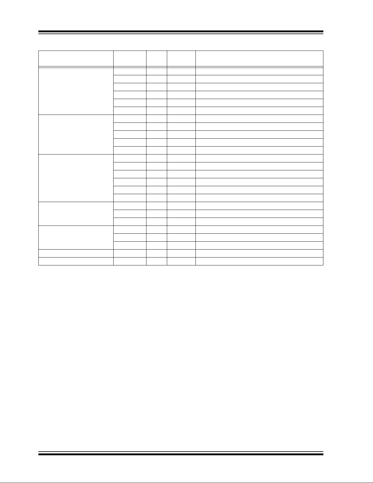
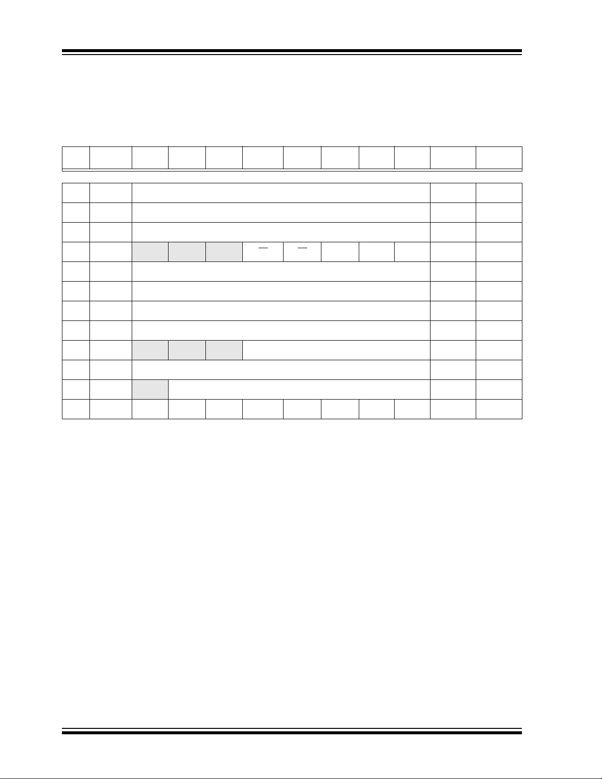
TABLE 1: PIC12/16(L)F161X FAMILY TYPES
Packages:
• PIC12(L)F1612:
- 8-pin: PDIP, SOIC, DFN
• PIC16(L)F1613:
- 14-pin: PDIP, SOIC, TSSOP
- 16-pin: QFN (4x4x0.9)
Debug Features:
• In-Circuit Debug (ICD):
- Integrated: supports all services
- Header: not required
•Emulation:
- Header: supports all devices
Device
Data Sheet Index
PIC12(L)F1612 (A) 2048 256 6 1/1 1 4 1 2/0 1 0 2/3 0 Y Y 0 0 0 I/H
PIC16(L)F1613 (A) 2048 256 12 1/1 2 8 1 2/0 1 0 2/3 0 Y Y 0 0 0 I/H
PIC16(L)F1614 (B) 4096 512 12 1/3 2 8 1 2/2 1 2 2/3 1 Y Y 1 1 1 I/H
PIC16(L)F1615 (C) 8192 1024 12 1/3 2 8 1 2/2 1 4 2/3 1 Y Y 1 1 1 I/H
PIC16(L)F1618 (B) 4096 512 18 1/3 2 12 1 2/2 1 2 2/3 1 Y Y 1 1 1 I/H
PIC16(L)F1619 (C) 8192 1024 18 1/3 2 12 1 2/2 1 4 2/3 1 Y Y 1 1 1 I/H
Note 1: Debugging Methods: (I) – Integrated on Chip; (H) – via ICD Header; E – using Emulation Product.
Data Sheet Index:
A. DS40001737 PIC12(L)F1612/16(L)F1613 Data Sheet, 8/14-Pin, 8-bit Flash Microcontrollers
B. Future Release PIC16(L)F1614/8 Data Sheet, 14/20-Pin, 8-bit Flash Microcontrollers
C. Future Release PIC16(L)F1615/9 Data Sheet, 14/20-Pin, 8-bit Flash Microcontrollers
(W)
(bytes)
Data SRAM
Program Memory Flash
I/O Pins
Comparators
8-bit/16-bit Timers
10-bit ADC (ch)
Zero-Cross Detect
CCP/10-bit PWM
CLC
CWG
SMT/HLT
Timer
Angular Timer
Window Watchdog
Math Accelerator
CRC with Memory Scan
EUSART
C™/SPI
2
I
Note: For other small form-factor package availability and marking information, please visit
http://www.microchip.com/packaging or contact your local sales office.
(1)
Debug
DS40001737A-page 2 Preliminary 2014 Microchip Technology Inc.
PIC12(L)F1612/16(L)F1613
1
2
3
4
8
7
6
5
VDD
RA5
RA3
V
SS
RA0
RA1
RA2
Note: See Table 2 for location of all peripheral functions.
RA4
PIC12F1612
PIC12LF1612
PIC16F1613
1
2
3
4
14
13
12
11
5
6
7
10
9
8
VDD
RA5
RA4
RA3
RC5
RC4
V
SS
RA0
RA1
RA2
RC0
RC1
RC2
RC3
Note: See Table 3 for location of all peripheral functions.
PIC16LF1613
PIC16F1613
PIC16LF1613
RA0
RA1
RA2
RC0
9
10
11
12
5
6
RC4
RC3
RC1
RC2
7
8
2
3
1
4
RA5
RA4
RA3/
MCLR/VPP
RC5
15
16
13
14
NC
VDD
NC
VSS
Note 1: See Ta bl e 3 for location of all peripheral functions.
2: For the QFN package, it is recommended that the bottom pad be connected to V
SS.
PIN DIAGRAMS
Pin Diagram – 8-PIN PDIP, SOIC, DFN, UDFN
Pin Diagram – 14-PIN PDIP, SOIC, TSSOP
Pin Diagram –
2014 Microchip Technology Inc. Preliminary DS40001737A-page 3
16-PIN QFN
PIC12(L)F1612/16(L)F1613
PIN ALLOCATION TABLE
TABLE 2: 8-PIN ALLOCATION TABLE FOR PIC12(L)F1612
I/O
RA0 7 AN0 DAC1OUT1 C1IN+ — CCP2 CWG1B — IOC — Y ICSPDAT
RA1 6 AN1 VREF+ C1IN0- — — — ZCD1OUT IOC — Y ICSPCLK
RA2 5 AN2 — C1OUT T0CKI
RA3 4 — — — T1G
RA4 3 AN3 — C1IN1- T1G — CWG1B — IOC SMTSIG1 Y CLKOUT
RA5 2 — — — T1CKI
VDD 1 — — — — — — — — — — VDD
Vss 8 — — — — — — — — — — VSS
Note 1: Alternate pin function selected with the APFCON register (Register 12-1).
A/D
Reference
8-Pin PDIP/SOIC/DFN
Comparator
Timers
T4IN
(1)
T6IN
T2IN
CCP
(1)
CCP1
— —
CCP1 CWG1A — IOC SMTWIN1 Y CLKIN
CWG1A
CWG1IN
CWG
(1)
ZCD
ZCD1IN INT
—
IOC
IOC SMTWIN2 Y
Interrupt
SMT
SMTSIG2 Y —
Pull-up
MCLR
VPP
TABLE 3: 14-PIN AND 16-PIN ALLOCATION TABLE FOR PIC16(L)F1613
I/O
14-Pin PDIP/SOIC/TSSOP
RA0 13 12 AN0 DAC1OUT1 C1IN+ — — — — IOC — Y ICSPDAT
RA1 12 11 AN1 VREF+ C1IN0-
RA2 11 10 AN2 — C1OUT T0CKI — CWG1IN ZCD1IN INT
RA3 4 3 — — — T1G
RA4 3 2 AN3 — — T1G — — — IOC SMTSIG1 Y CLKOUT
RA5 2 1 — — — T1CKI
RC0 10 9 AN4 — C2IN+ — — — — IOC — Y —
RC1 9 8 AN5 — C1IN1-
RC2 8 7 AN6 — C1IN2-
RC3 7 6 AN7 — C1IN3-
RC4 6 5 — — C2OUT — — CWG1B — IOC — Y —
RC5 5 4 — — — — CCP1 CWG1A — IOC — Y —
VDD 1 16 — — — — — — — — — — VDD
VSS 14 13 — — — — — — — — ——VSS
Note 1: Alternate pin function selected with the APFCON register (Register 12-1).
A/D
16-Pin QFN
Reference
Comparator
C2IN0-
C2IN1-
C2IN2-
C2IN3-
Timers
— — — ZCD1OUT IOC — Y ICSPCLK
(1)
T6IN
T2IN
T4IN — — — IOC SMTSIG2 Y —
— — CWG1D — IOC — Y —
— CCP2 CWG1C — IOC — Y —
CCP
— — — IOC SMTWIN2 Y
(1)
CCP2
CWG
— — IOC SMTWIN1 Y CLKIN
ZCD
Interrupt
IOC
SMT
— Y —
Pull-up
MCLR
Basic
Basic
VPP
DS40001737A-page 4 Preliminary 2014 Microchip Technology Inc.

PIC12(L)F1612/16(L)F1613
TABLE OF CONTENTS
Device Overview ................................................................................................................................................................................... 7
Enhanced Mid-Range CPU ................................................................................................................................................................. 13
Memory Organization .......................................................................................................................................................................... 15
Device Configuration ........................................................................................................................................................................... 47
Oscillator Module ................................................................................................................................................................................ 54
Resets ................................................................................................................................................................................................. 65
Interrupts ............................................................................................................................................................................................. 73
Power-Down Mode (Sleep) ................................................................................................................................................................. 88
Windowed Watchdog Timer (WDT) .................................................................................................................................................... 91
Flash Program Memory Control.......................................................................................................................................................... 99
Cyclic Redundancy Check (CRC) Module ........................................................................................................................................ 115
I/O Ports ............................................................................................................................................................................................ 127
Interrupt-On-Change ......................................................................................................................................................................... 141
Fixed Voltage Reference (FVR)........................................................................................................................................................ 146
Temperature Indicator Module.......................................................................................................................................................... 149
Analog-to-Digital Converter (ADC) Module ....................................................................................................................................... 151
8-bit Digital-to-Analog Converter (DAC1) Module ............................................................................................................................. 165
Comparator Module .......................................................................................................................................................................... 169
Zero-Cross Detection (ZCD) Module ................................................................................................................................................ 177
Timer0 Module .................................................................................................................................................................................. 181
Timer1 Module with Gate Control ..................................................................................................................................................... 184
Timer2/4/6 Module ............................................................................................................................................................................ 195
Capture/Compare/PWM Modules ..................................................................................................................................................... 214
Complementary Waveform Generator (CWG) Module ..................................................................................................................... 228
Signal Measurement Timer (SMTx) .................................................................................................................................................. 255
In-Circuit Serial Programming™ (ICSP™) ........................................................................................................................................ 299
Instruction Set Summary................................................................................................................................................................... 301
Electrical Specifications .................................................................................................................................................................... 315
DC and AC Characteristics Graphs and Charts................................................................................................................................ 339
Development Support ....................................................................................................................................................................... 357
Packaging Information ...................................................................................................................................................................... 361
Appendix A: Data Sheet Revision History......................................................................................................................................... 380
The Microchip Web Site.................................................................................................................................................................... 381
Customer Change Notification Service ............................................................................................................................................. 381
Customer Support ............................................................................................................................................................................. 381
Product Identification System ........................................................................................................................................................... 382
2014 Microchip Technology Inc. Preliminary DS40001737A-page 5

PIC12(L)F1612/16(L)F1613
TO OUR VALUED CUSTOMERS
It is our intention to provide our valued customers with the best documentation possible to ensure successful use of your Microchip
products. To this end, we will continue to improve our publications to better suit your needs. Our publications will be refined and
enhanced as new volumes and updates are introduced.
If you have any questions or comments regarding this publication, please contact the Marketing Communications Department via
E-mail at docerrors@microchip.com or fax the Reader Response Form in the back of this data sheet to (480) 792-4150. We
welcome your feedback.
Most Current Data Sheet
To obtain the most up-to-date version of this data sheet, please register at our Worldwide Web site at:
http://www.microchip.com
You can determine the version of a data sheet by examining its literature number found on the bottom outside corner of any page.
The last character of the literature number is the version number, (e.g., DS30000A is version A of document DS30000).
Errata
An errata sheet, describing minor operational differences from the data sheet and recommended workarounds, may exist for current
devices. As device/documentation issues become known to us, we will publish an errata sheet. The errata will specify the revision
of silicon and revision of document to which it applies.
To determine if an errata sheet exists for a particular device, please check with one of the following:
• Microchip’s Worldwide Web site; http://www.microchip.com
• Your local Microchip sales office (see last page)
When contacting a sales office, please specify which device, revision of silicon and data sheet (include literature number) you are
using.
Customer Notification System
Register on our web site at www.microchip.com to receive the most current information on all of our products.
DS40001737A-page 6 Preliminary 2014 Microchip Technology Inc.
PIC12(L)F1612/16(L)F1613
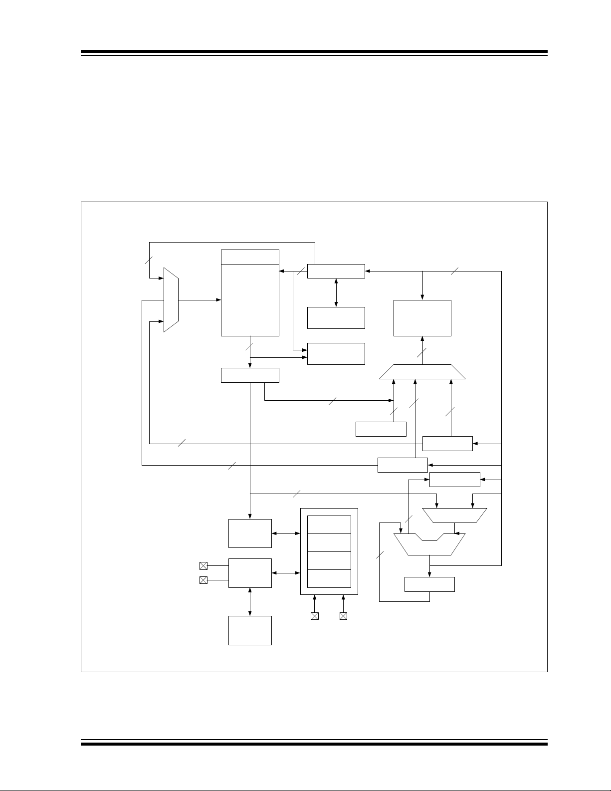
1.0 DEVICE OVERVIEW
The PIC12(L)F1612/16(L)F1613 are described within this
data sheet. The block diagram of these devices are
shown in Figure 1-1, the available peripherals are shown
in Table 1-1, and the pin out descriptions are shown in
Tables 1-2 and 1-3.
TABLE 1-1: DEVICE PERIPHERAL
SUMMARY
Peripheral
PIC12(L)F1612
PIC16(L)F1613
Analog-to-Digital Converter (ADC) ●●
Complementary Wave Generator (CWG) ●●
Cyclic Redundancy Check (CRC) ●●
Digital-to-Analog Converter (DAC) ●●
Fixed Voltage Reference (FVR) ●●
Temperature Indicator ●●
Windowed Watchdog Timer (WDT) ●●
Zero Cross Detection (ZCD) ●●
Capture/Compare/PWM (CCP) Modules
CCP1 ●●
CCP2 ●●
Comparators
C1 ●●
C2 ●
Signal Measurement Timer (SMT)
SMT1 ●●
SMT2 ●●
Timers
Timer0 ●●
Timer1 ●●
Timer2 ●●
Timer4 ●●
Timer6 ●●
2014 Microchip Technology Inc. Preliminary DS40001737A-page 7
PIC12(L)F1612/16(L)F1613
Rev. 10 -000 039F
12/19 /201 3
CLKOUT
CLKIN
RAM
CPU
(Note 3)
Timing
Generation
INTRC
Oscillator
MCLR
Program
Flash Mem ory
FVR
ADC
10-bit
Temp
Indicator
TMR0TMR1TMR2
CCP1CCP2ZCD1CWG1
PORTA
DACC1
CRC
TMR4TMR6 C2
SMT2 SMT 1
PORTC
(4)
(4)
Note 1: See applicable chapters for more information on peripherals.
2: See Table 1-1 for peripherals available on specific devices.
3: See Figure 2-1.
4: PIC16(L)F1613 only.
FIGURE 1-1: PIC12(L)F1612/16(L)F1613 BLOCK DIAGRAM
DS40001737A-page 8 Preliminary 2014 Microchip Technology Inc.
PIC12(L)F1612/16(L)F1613
TABLE 1-2: PIC12(L)F1612 PINOUT DESCRIPTION
Name Function
RA0/AN0/C1IN+/DAC1OUT1/
CCP2/CWG1B
(1)
/
ICSPDAT
RA0
AN0 AN — ADC Channel input.
C1IN+ AN — Comparator positive input.
Input
Typ e
TTL/ST CMOS/OD
DAC1OUT1 — AN Digital-to-Analog Converter output.
CCP2 TTL/ST — Capture/Compare/PWM2.
CWG1B TTL/ST — CWG complementary output B.
ICSPDAT ST CMOS ICSP™ Data I/O.
RA1/AN1/V
REF+/C1IN0-/
ZCD1OUT/ICSPCLK
RA1 TTL/ST CMOS/OD General purpose I/O.
AN1 AN — ADC Channel input.
REF+AN — Voltage Reference input.
V
C1IN0- AN — Comparator negative input.
ZCD1OUT — CMOS Zero-Cross Detect output.
ICSPCLK ST — ICSP Programming Clock.
RA2/AN2/C1OUT/T0CKI/T4IN/
CCP1
(1)
/CWG1A
(1)
/
CWG1IN/ZCD1IN/INT/SMTSIG2
RA2 TTL/ST CMOS/OD General purpose I/O.
AN2 AN — ADC Channel input.
C1OUT — CMOS/OD Comparator output.
T0CKI TTL/ST — Timer0 clock input.
T4IN TTL/ST — Timer4 input.
CCP1 TTL/ST CMOS/OD Capture/Compare/PWM1.
CWG1A ——CWG complementary output A.
CWG1IN TTL/ST — CWG complementary input.
ZCD1IN AN — Zero-Cross Detect input.
INT TTL/ST — External interrupt.
SMTSIG2 TTL/ST — SMT2 signal input.
(1)
PP/T1G
RA3/V
SMTWIN2/MCLR
/T6IN/
RA3 TTL/ST — General purpose input with IOC and WPU.
PP HV — Programming voltage.
V
T1G TTL/ST — Timer1 Gate input.
T6IN TTL/ST — Timer6 input.
SMTWIN2 TTL/ST — SMT2 window input.
TTL/ST — Master Clear with internal pull-up.
RA4/AN3/C1IN1-/T1G
(1)
CWG1B
/SMTSIG1/
CLKOUT
(1)
/
RA4 TTL/ST CMOS/OD General purpose I/O.
AN3 AN — ADC Channel input.
C1IN1- AN — Comparator negative input.
MCLR
T1G TTL/ST — Timer1 Gate input.
CWG1B — CMOS/OD CWG complementary output A.
SMTSIG1 TTL/ST — SMT1 signal input.
CLKOUT — CMOS F
Legend: AN = Analog input or output CMOS = CMOS compatible input or output OD = Open-Drain
Note 1: Alternate pin function selected with the APFCON register (Register 12-1).
TTL = TTL compatible input ST = Schmitt Trigger input with CMOS levels I
HV = High Voltage XTAL = Crystal levels
Output
Type
General purpose I/O.
OSC/4 output.
2
C™ = Schmitt Trigger input with I2C™
Description
2014 Microchip Technology Inc. Preliminary DS40001737A-page 9
PIC12(L)F1612/16(L)F1613
TABLE 1-2: PIC12(L)F1612 PINOUT DESCRIPTION (CONTINUED)
Name Function
RA5/CLKIN/T1CKI/T2IN/
(1)
CCP1
/CWG1A
SMTWIN1
DD VDD Power — Positive supply.
V
SS VSS Power — Ground reference.
V
Legend: AN = Analog input or output CMOS = CMOS compatible input or output OD = Open-Drain
Note 1: Alternate pin function selected with the APFCON register (Register 12-1).
(1)
/
TTL = TTL compatible input ST = Schmitt Trigger input with CMOS levels I
HV = High Voltage XTAL = Crystal levels
RA5 TTL/ST CMOS/OD General purpose I/O.
CLKIN CMOS — External clock input (EC mode).
T1CKI TTL/ST — Timer1 clock input.
T2IN TTL/ST — Timer2 input.
CCP1 TTL/ST CMOS/OD Capture/Compare/PWM1.
CWG1A — CMOS/OD CWG complementary output A.
SMTWIN1 TTL/ST — SMT1 window input.
Input
Typ e
Output
Type
Description
2
C™ = Schmitt Trigger input with I2C™
DS40001737A-page 10 Preliminary 2014 Microchip Technology Inc.
PIC12(L)F1612/16(L)F1613
TABLE 1-3: PIC16(L)F1613 PINOUT DESCRIPTION
Name Function
RA0/AN0/C1IN+/DAC1OUT1/
ICSPDAT
RA0
AN0 AN — ADC Channel input.
Input
Typ e
TTL/ST
C1IN+ AN — Comparator positive input.
DAC1OUT1 — AN Digital-to-Analog Converter output.
ICSPDAT ST CMOS ICSP™ Data I/O.
RA1/AN1/V
REF+/C1IN0-/C2IN0-/
ZCD1OUT/ICSPCLK
RA1 TTL/ST CMOS/OD General purpose I/O.
AN1 AN — ADC Channel input.
REF+ AN — Voltage Reference input.
V
C1IN0- AN — Comparator negative input.
C2IN0- AN CMOS/OD Comparator negative input.
ZCD1OUT — — Zero-Cross Detect output.
ICSPCLK ST ICSP Programming Clock.
RA2/AN2/C1OUT/T0CKI/
CWG1IN/ZCD1IN/INT
RA2 TTL/ST CMOS/OD General purpose I/O.
AN2 AN — ADC Channel input.
C1OUT — CMOS/OD Comparator output.
T0CKI TTL/ST — Timer0 clock input.
CWG1IN TTL/ST — CWG complementary input.
ZCD1IN AN — Zero-Cross Detect input.
INT TTL/ST — External interrupt.
(1)
PP/T1G
RA3/V
SMTWIN2/M
CLR
/T6IN/
RA3 TTL/ST — General purpose input with IOC and WPU.
V
PP HV — Programming voltage.
T1G TTL/ST — Timer1 Gate input.
T6IN TTL/ST — Timer6 input.
SMTWIN2 TTL/ST — SMT2 window input.
TTL/ST — Master Clear with internal pull-up.
RA4/AN3/T1G
CLKOUT
(1)
/SMTSIG1/
MCLR
RA4 TTL/ST CMOS/OD General purpose I/O.
AN3 AN — ADC Channel input.
T1G TTL/ST — Timer1 Gate input.
SMTSIG1 TTL/ST — SMT1 signal input.
CLKOUT — CMOS F
RA5/CLKIN/T1CKI/T2IN/
(1)
/SMTWIN1
CCP2
RA5 TTL/ST CMOS/OD General purpose I/O.
CLKIN CMOS — External clock input (EC mode).
T1CKI TTL/ST — Timer1 clock input.
T2IN TTL/ST — Timer2 input.
CCP2 TTL/ST CMOS/OD Capture/Compare/PWM2.
SMTWIN1 TTL/ST — SMT1 window input.
RC0/AN4/C2IN+ RC0 TTL/ST CMOS/OD General purpose I/O.
AN4 AN — ADC Channel input.
C2IN+ AN — Comparator positive input.
Legend: AN = Analog input or output CMOS = CMOS compatible input or output OD = Open-Drain
Note 1: Alternate pin function selected with the APFCON register (Register 12-1).
TTL = TTL compatible input ST = Schmitt Trigger input with CMOS levels I
HV = High Voltage XTAL = Crystal levels
Output
Typ e
CMOS/OD General purpose I/O.
OSC/4 output.
2
C™ = Schmitt Trigger input with I2C™
Description
2014 Microchip Technology Inc. Preliminary DS40001737A-page 11
PIC12(L)F1612/16(L)F1613
TABLE 1-3: PIC16(L)F1613 PINOUT DESCRIPTION (CONTINUED)
Name Function
RC1/AN5/C1IN1-/C2IN1-/T4IN/
SMTSIG2
RC2/AN6/C1IN2-/C2IN2-/
CWG1D
RC3/AN7/C1IN3-/C2IN3-/
(1)
/CWG1C
CCP2
RC4/C2OUT/CWG1B RC4 TTL/ST CMOS/OD General purpose I/O.
RC5/CCP1/CWG1A RC5 TTL/ST CMOS/OD General purpose I/O.
DD VDD Power — Positive supply.
V
SS VSS Power — Ground reference.
V
Legend: AN = Analog input or output CMOS = CMOS compatible input or output OD = Open-Drain
Note 1: Alternate pin function selected with the APFCON register (Register 12-1).
TTL = TTL compatible input ST = Schmitt Trigger input with CMOS levels I
HV = High Voltage XTAL = Crystal levels
RC1 TTL/ST CMOS/OD General purpose I/O.
AN5 AN — ADC Channel input.
C1IN1- AN — Comparator negative input.
C2IN1- AN — Comparator negative input.
T4IN TTL/ST — Timer4 input.
SMTSIG2 TTL/ST — SMT2 signal input.
RC2 TTL/ST CMOS/OD General purpose I/O.
AN6 AN — ADC Channel input.
C1IN2- AN — Comparator negative input.
C2IN2- AN — Comparator negative input.
CWG1D — CMOS/OD CWG complementary output D.
RC3 TTL/ST — General purpose input with IOC and WPU.
AN7 AN — ADC Channel input.
C1IN3- AN — Comparator negative input.
C2IN3- AN — Comparator negative input.
CCP2 TTL/ST CMOS/OD Capture/Compare/PWM2.
CWG1C — CMOS/OD CWG complementary output C.
C2OUT — CMOS/OD Comparator output.
CWG1B — CMOS/OD CWG complementary output B.
CCP1 TTL/ST CMOS/OD Capture/Compare/PWM1.
CWG1A — CMOS/OD CWG complementary output A.
Input
Typ e
Output
Typ e
Description
2
C™ = Schmitt Trigger input with I2C™
DS40001737A-page 12 Preliminary 2014 Microchip Technology Inc.
PIC12(L)F1612/16(L)F1613
15
15
15
15
8
8
8
12
14
7
5
3
Program Counter
MUX
Addr MUX
16-Level Stack
(15-bit)
Program Memory
Read (PMR)
Instruction Reg
Configuration
FSR0 Reg
FSR1 Reg
BSR Reg
STATUS Reg
RAM
WReg
Power-up
Timer
Power-on
Reset
Watchdog
Timer
Brown-out
Reset
Instruction
Decode and
Control
Timing
Generation
Internal
Oscillator
Block
ALU
Flash
Program
Memory
MUX
Data Bus
Program
Bus
Direct Addr
Indirect
Addr
RAM Addr
CLKIN
CLKOUT
V
DD VSS
Rev. 10-000055A
7/30/2013
12
12
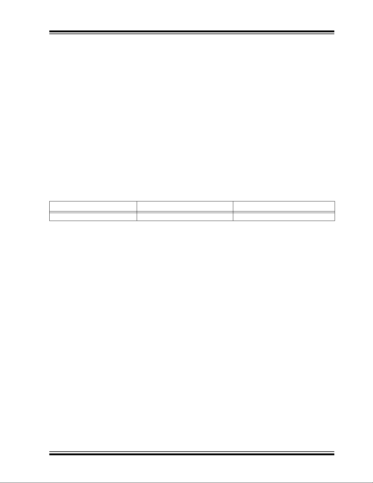
2.0 ENHANCED MID-RANGE CPU
This family of devices contain an enhanced mid-range
8-bit CPU core. The CPU has 49 instructions. Interrupt
capability includes automatic context saving. The
hardware stack is 16 levels deep and has Overflow and
Underflow Reset capability. Direct, Indirect, and
Relative addressing modes are available. Two File
Select Registers (FSRs) provide the ability to read
program and data memory.
FIGURE 2-1: CORE BLOCK DIAGRAM
• Automatic Interrupt Context Saving
• 16-level Stack with Overflow and Underflow
• File Select Registers
• Instruction Set
2014 Microchip Technology Inc. Preliminary DS40001737A-page 13

PIC12(L)F1612/16(L)F1613
2.1 Automatic Interrupt Context Saving
During interrupts, certain registers are automatically
saved in shadow registers and restored when returning
from the interrupt. This saves stack space and user
code. See Section 7.5 “Automatic Context Saving”,
for more information.
2.2 16-Level Stack with Overflow and Underflow
These devices have a hardware stack memory 15 bits
wide and 16 words deep. A Stack Overflow or Underflow will set the appropriate bit (STKOVF or STKUNF)
in the PCON register, and if enabled, will cause a software Reset. See section Section 3.4 “Stack” for more
details.
2.3 File Select Registers
There are two 16-bit File Select Registers (FSR). FSRs
can access all file registers and program memory,
which allows one Data Pointer for all memory. When an
FSR points to program memory, there is one additional
instruction cycle in instructions using INDF to allow the
data to be fetched. General purpose memory can now
also be addressed linearly, providing the ability to
access contiguous data larger than 80 bytes. There are
also new instructions to support the FSRs. See
Section 3.5 “Indirect Addressing” for more details.
2.4 Instruction Set
There are 49 instructions for the enhanced mid-range
CPU to support the features of the CPU. See
Section 27.0 “Instruction Set Summary” for more
details.
DS40001737A-page 14 Preliminary 2014 Microchip Technology Inc.
PIC12(L)F1612/16(L)F1613
3.0 MEMORY ORGANIZATION
These devices contain the following types of memory:
• Program Memory
- Configuration Words
- Device ID
-User ID
- Flash Program Memory
• Data Memory
- Core Registers
- Special Function Registers
- General Purpose RAM
- Common RAM
The following features are associated with access and
control of program memory and data memory:
• PCL and PCLATH
•Stack
• Indirect Addressing
3.1 Program Memory Organization
The enhanced mid-range core has a 15-bit program
counter capable of addressing a 32K x 14 program
memory space. Table 3-1 shows the memory sizes
implemented. Accessing a location above these
boundaries will cause a wrap-around within the
implemented memory space. The Reset vector is at
0000h and the interrupt vector is at 0004h (See
Figure 3-1).
TABLE 3-1: DEVICE SIZES AND ADDRESSES
Device Program Memory Space (Words) Last Program Memory Address
PIC12(L)F1612/16(L)F1613 2,048 07FFh
2014 Microchip Technology Inc. Preliminary DS40001737A-page 15
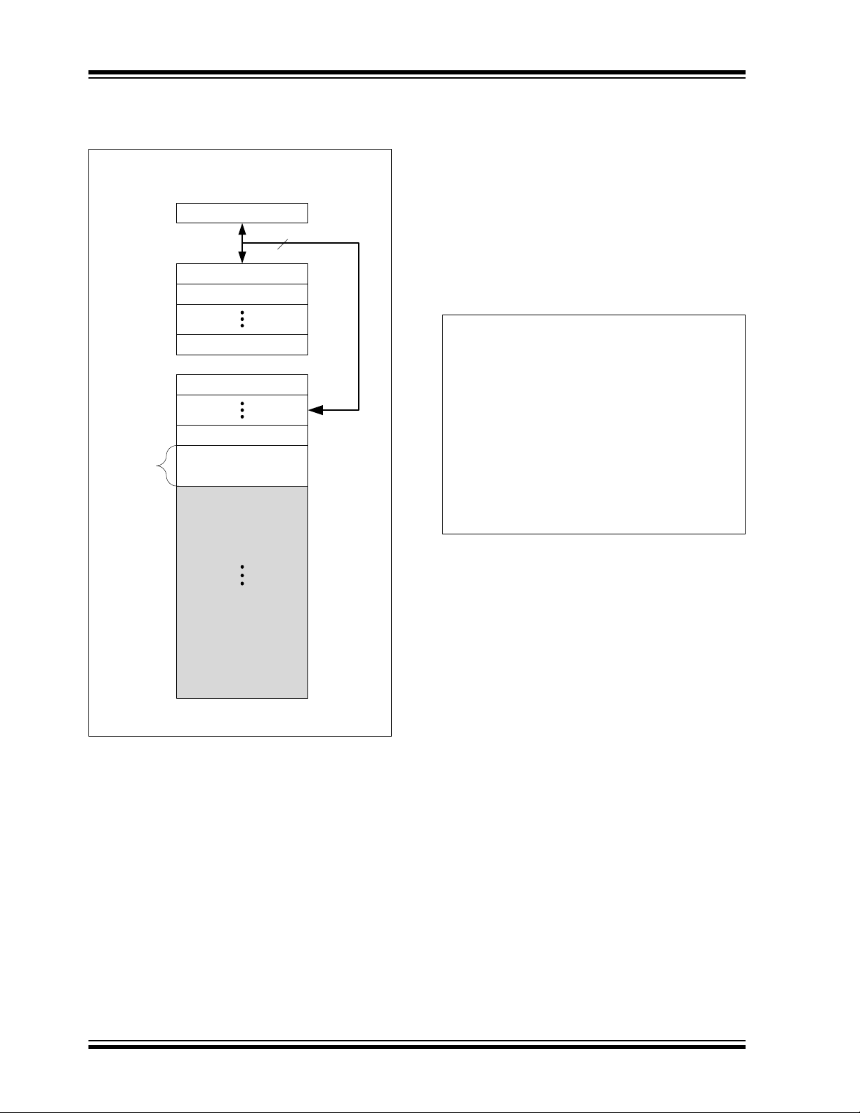
PIC12(L)F1612/16(L)F1613
Stack Level 0
Stack Level 15
Stack Level 1
Reset Vector
PC<14:0>
Interrupt Vector
Page 0
Rollover to Page 0
Rollover to Page 0
0000h
0004h
0005h
07FFh
0800h
7FFFh
CALL, CALLW
RETURN, RETLW
Interrupt, RETFIE
On-chip
Program
Memory
15
Rev. 10-000040C
7/30/2013
constants
BRW ;Add Index in W to
;program counter to
;select data
RETLW DATA0 ;Index0 data
RETLW DATA1 ;Index1 data
RETLW DATA2
RETLW DATA3
my_function
;… LOTS OF CODE…
MOVLW DATA_INDEX
call constants
;… THE CONSTANT IS IN W
FIGURE 3-1: PROGRAM MEMORY MAP
AND STACK FOR
PIC12(L)F1612/16(L)F1613
3.1.1 READING PROGRAM MEMORY AS DATA
There are two methods of accessing constants in program memory. The first method is to use tables of
RETLW instructions. The second method is to set an
FSR to point to the program memory.
3.1.1.1 RETLW Instruction
The RETLW instruction can be used to provide access
to tables of constants. The recommended way to create
such a table is shown in Example 3-1.
EXAMPLE 3-1: RETLW INSTRUCTION
The BRW instruction makes this type of table very simple to implement. If your code must remain portable
with previous generations of microcontrollers, then the
BRW instruction is not available, so the older table read
method must be used.
DS40001737A-page 16 Preliminary 2014 Microchip Technology Inc.

PIC12(L)F1612/16(L)F1613
constants
RETLW DATA0 ;Index0 data
RETLW DATA1 ;Index1 data
RETLW DATA2
RETLW DATA3
my_function
;… LOTS OF CODE…
MOVLW LOW constants
MOVWF FSR1L
MOVLW HIGH constants
MOVWF FSR1H
MOVIW 0[FSR1]
;THE PROGRAM MEMORY IS IN W
3.1.1.2 Indirect Read with FSR
The program memory can be accessed as data by setting bit 7 of the FSRxH register and reading the matching INDFx register. The MOVIW instruction will place the
lower eight bits of the addressed word in the W register.
Writes to the program memory cannot be performed via
the INDF registers. Instructions that access the program memory via the FSR require one extra instruction
cycle to complete. Example 3-2 demonstrates accessing the program memory via an FSR.
The HIGH operator will set bit<7> if a label points to a
location in program memory.
EXAMPLE 3-2: ACCESSING PROGRAM
MEMORY VIA FSR
2014 Microchip Technology Inc. Preliminary DS40001737A-page 17
PIC12(L)F1612/16(L)F1613
Addresses BANKx
x00h or x80h INDF0
x01h or x81h INDF1
x02h or x82h PCL
x03h or x83h STATUS
x04h or x84h FSR0L
x05h or x85h FSR0H
x06h or x86h FSR1L
x07h or x87h FSR1H
x08h or x88h BSR
x09h or x89h WREG
x0Ah or x8Ah PCLATH
x0Bh or x8Bh INTCON
3.2 Data Memory Organization
The data memory is partitioned in 32 memory banks
with 128 bytes in a bank. Each bank consists of
(Figure 3-2):
• 12 core registers
• 20 Special Function Registers (SFR)
• Up to 80 bytes of General Purpose RAM (GPR)
• 16 bytes of common RAM
The active bank is selected by writing the bank number
into the Bank Select Register (BSR). Unimplemented
memory will read as ‘0’. All data memory can be
accessed either directly (via instructions that use the
file registers) or indirectly via the two File Select
Registers (FSR). See Section 3.5 “Indirect
Addressing” for more information.
Data memory uses a 12-bit address. The upper five bits
of the address define the Bank address and the lower
seven bits select the registers/RAM in that bank.
3.2.1 CORE REGISTERS
The core registers contain the registers that directly
affect the basic operation. The core registers occupy
the first 12 addresses of every data memory bank
(addresses x00h/x08h through x0Bh/x8Bh). These
registers are listed below in Ta b l e 3 -2 . For detailed
information, see Tab le 3 -9 .
TABLE 3-2: CORE REGISTERS
DS40001737A-page 18 Preliminary 2014 Microchip Technology Inc.
PIC12(L)F1612/16(L)F1613
3.2.1.1 STATUS Register
The STATUS register, shown in Register 3-1, contains:
• the arithmetic status of the ALU
• the Reset status
The STATUS register can be the destination for any
instruction, like any other register. If the STATUS
register is the destination for an instruction that affects
the Z, DC or C bits, then the write to these three bits is
disabled. These bits are set or cleared according to the
device logic. Furthermore, the TO
writable. Therefore, the result of an instruction with the
STATUS register as destination may be different than
intended.
and PD bits are not
For example, CLRF STATUS will clear the upper three
bits and set the Z bit. This leaves the STATUS register
as ‘000u u1uu’ (where u = unchanged).
It is recommended, therefore, that only BCF, BSF,
SWAPF and MOVWF instructions are used to alter the
STATUS register, because these instructions do not
affect any Status bits. For other instructions not
affecting any Status bits (Refer to Section 27.0
“Instruction Set Summary”).
Note 1: The C and DC bits operate as Borrow
and Digit Borrow out bits, respectively, in
subtraction.
REGISTER 3-1: STATUS: STATUS REGISTER
U-0 U-0 U-0 R-1/q R-1/q R/W-0/u R/W-0/u R/W-0/u
— — —
bit 7 bit 0
Legend:
R = Readable bit W = Writable bit U = Unimplemented bit, read as ‘0’
u = Bit is unchanged x = Bit is unknown -n/n = Value at POR and BOR/Value at all other Resets
‘1’ = Bit is set ‘0’ = Bit is cleared q = Value depends on condition
TO
PD ZDC
(1)
(1)
C
bit 7-5 Unimplemented: Read as ‘0’
bit 4 TO
bit 3 PD
bit 2 Z: Zero bit
bit 1 DC: Digit Carry/Digit Borrow bit (ADDWF, ADDLW, SUBLW, SUBWF instructions)
bit 0 C: Carry/Borrow
Note 1: For Borrow, the polarity is reversed. A subtraction is executed by adding the two’s complement of the
second operand. For rotate (RRF, RLF) instructions, this bit is loaded with either the high-order or low-order
bit of the source register.
: Time-Out bit
1 = After power-up, CLRWDT instruction or SLEEP instruction
0 = A WDT time-out occurred
: Power-Down bit
1 = After power-up or by the CLRWDT instruction
0 = By execution of the SLEEP instruction
1 = The result of an arithmetic or logic operation is zero
0 = The result of an arithmetic or logic operation is not zero
1 = A carry-out from the 4th low-order bit of the result occurred
0 = No carry-out from the 4th low-order bit of the result
(1)
bit
(ADDWF, ADDLW, SUBLW, SUBWF instructions)
1 = A carry-out from the Most Significant bit of the result occurred
0 = No carry-out from the Most Significant bit of the result occurred
(1)
(1)
2014 Microchip Technology Inc. Preliminary DS40001737A-page 19
PIC12(L)F1612/16(L)F1613
Memory Region7-bit Bank Offset
00h
0Bh
0Ch
1Fh
20h
6Fh
7Fh
70h
Core Registers
(12 bytes)
Special Function Registers
(20 bytes maximum)
General Purpose RAM
(80 bytes maximum)
Common RAM
(16 bytes)
Rev. 10-000041A
7/30/2013
3.2.2 SPECIAL FUNCTION REGISTER
The Special Function Registers are registers used by
the application to control the desired operation of
peripheral functions in the device. The Special Function
Registers occupy the 20 bytes after the core registers of
every data memory bank (addresses x0Ch/x8Ch
through x1Fh/x9Fh). The registers associated with the
operation of the peripherals are described in the appropriate peripheral chapter of this data sheet.
3.2.3 GENERAL PURPOSE RAM
There are up to 80 bytes of GPR in each data memory
bank. The Special Function Registers occupy the 20
bytes after the core registers of every data memory
bank (addresses x0Ch/x8Ch through x1Fh/x9Fh).
3.2.3.1 Linear Access to GPR
The general purpose RAM can be accessed in a
non-banked method via the FSRs. This can simplify
access to large memory structures. See Section 3.5.2
“Linear Data Memory” for more information.
3.2.4 COMMON RAM
There are 16 bytes of common RAM accessible from all
banks.
FIGURE 3-2: BANKED MEMORY
PARTITIONING
3.2.5 DEVICE MEMORY MAPS
The memory maps for PIC12(L)F1612/16(L)F1613 are
as shown in Ta bl e 3 -5 through Tab l e 3 - 8.
DS40001737A-page 20 Preliminary 2014 Microchip Technology Inc.
2014 Microchip Technology Inc. Preliminary DS40001737A-page 21
TABLE 3-3: PIC12(L)F1612 MEMORY MAP, BANK 1-7
BANK 0 BANK 1 BANK 2 BANK 3 BANK 4 BANK 5 BANK 6 BANK 7
000h
Core Registers
(Ta bl e 3- 2 )
00Bh 08Bh 10Bh 18Bh 20Bh 28Bh 30Bh 38Bh
00Ch PORTA 08Ch TRISA 10Ch LATA 18Ch ANSELA 20Ch WPUA 28Ch ODCONA 30Ch SLRCONA 38Ch INLVLA
00Dh
00Eh
00Fh
010h
011h PIR1 091h PIE1 111h CM1CON0 191h PMADRL 211h
012h PIR2 092h PIE2 112h CM1CON1 192h PMADRH 212h
013h PIR3 093h PIE3 113h
014h PIR4 094h PIE4 114h
015h TMR0 095h OPTION_REG 115h CMOUT 195h PMCON1 215h
016h
017h
018h
019h
01Ah
01Bh
01Ch
01Dh
01Eh
01Fh
020h
— 08Dh — 10Dh — 18Dh — 20Dh — 28Dh — 30Dh — 38Dh —
—08Eh—10Eh—18Eh—20Eh—28Eh—30Eh—38Eh—
—08Fh—10Fh—18Fh—20Fh—28Fh—30Fh—38Fh—
—090h—110h—190h—210h—290h
TMR1L 096h PCON 116h BORCON 196h PMCON2 216h
TMR1H 097h
T1CON 098h OSCTUNE 118h
T1GCON 099h OSCCON 119h
TMR2 09Ah OSCSTAT 11Ah
PR2 09BhADRESL11Bh
T2CON 09Ch ADRESH 11Ch
T2HLT
T2CLKCON
T2RST
080h
Core Registers
(Ta bl e 3- 2 )
— 117h FVRCON 197h VREGCON 217h
09Dh ADCON0 11Dh APFCON 19Dh
09Eh ADCON1 11Eh
09Fh ADCON2 11Fh
0A0h
100h
120h
Core Registers
(Table 3-2)
— 193h PMDATL 213h
— 194h PMDATH 214h
DAC1CON0
DAC1CON1
—19Ah
—19Bh
ZCD1CON
—
—19Fh
180h
198h
199h
19Ch
19Eh
1A0h
Core Registers
(Table 3-2)
—218h
—
—
—
—
—
—
—
200h
219h
21Ah
21Bh
21Ch
21Dh
21Eh
21Fh
220h
Core Registers
(Table 3-2)
—
—
—
—
—
—
—
—
—299h
—29Ah
—29Bh
— 29Ch — 31Ch
—
—
—
280h
Core Registers
(Table 3-2)
—
291h CCP1RL 311h
292h CCP1RH 312h
293h CCP1CON 313h
294h CCP1CAP 314h
295h
296h
297h
298h
29Dh
29Eh CCPTMRS 31Eh
29Fh
2A0h
—
— 316h — 396h
— 317h — 397h
CCP2RL
CCP2RH
CCP2CON
CCP2CAP
—
—
300h
Core Registers
(Table 3-2)
310h
315h
318h
319h — 399h
31Ah —39Ah—
31Bh
31Dh
31Fh
320h
— 390h —
—
—
—
—
—
— 398h
—
—
—
—
—
380h
Core Registers
(Table 3-2)
391h IOCAP
392h IOCAN
393h
394h
395h
39Bh
39Ch
39Dh
39Eh
39Fh
3A0h
IOCAF
—
—
—
—
—
—
—
—
—
—
—
PIC12(L)F1612/16(L)F1613
General
Purpose
Register
80 Bytes
06Fh
070h
Common RAM
07Fh 0FFh 17Fh 1FFh 27Fh 2FFh 37Fh 3FFh
Legend: = Unimplemented data memory locations, read as ‘0’.
0EFh
0F0h
General
Purpose
Register
80 Bytes
Common RAM
(Accesses
70h – 7Fh)
General
Purpose
Register
80 Bytes
16Fh 1EFh 26Fh 2EFh
170h
Common RAM
(Accesses
70h – 7Fh)
1F0h
Unimplemented
Read as ‘0’
Common RAM
(Accesses
70h – 7Fh)
270h
Unimplemented
Read as ‘0’
Common RAM
(Accesses
70h – 7Fh)
2F0h
Unimplemented
Read as ‘0’
Common RAM
(Accesses
70h – 7Fh)
Unimplemented
Read as ‘0’
36Fh 3EFh
370h
Common RAM
(Accesses
70h – 7Fh)
3F0h
Unimplemented
Read as ‘0’
Common RAM
(Accesses
70h – 7Fh)
DS40001737A-page 22 Preliminary 2014 Microchip Technology Inc.
TABLE 3-4: PIC16(L)F1613 MEMORY MAP, BANK 1-7
PIC12(L)F1612/16(L)F1613
BANK 0 BANK 1 BANK 2 BANK 3 BANK 4 BANK 5 BANK 6 BANK 7
000h
Core Registers
(Ta bl e 3- 2 )
00Bh 08Bh 10Bh 18Bh 20Bh 28Bh 30Bh 38Bh
00Ch PORTA 08Ch TRISA 10Ch LATA 18Ch ANSELA 20Ch WPUA 28Ch ODCONA 30Ch SLRCONA 38Ch INLVLA
00Dh
00Eh PORTC 08Eh TRISC 10Eh LATC 18Eh ANSELC 20Eh WPUC 28Eh ODCONC 30Eh SLRCONC 38Eh INLVLC
00Fh —08Fh—10Fh—18Fh—20Fh—28Fh—30Fh—38Fh—
010h
011h PIR1 091h PIE1 111h CM1CON0 191h PMADRL 211h
012h PIR2 092h PIE2 112h CM1CON1 192h PMADRH 212h
013h PIR3 093h PIE3 113h CM2CON0 193h PMDATL 213h
014h PIR4 094h PIE4 114h CM2CON1 194h PMDATH 214h
015h TMR0 095h OPTION_REG 115h CMOUT 195h PMCON1 215h
016h
017h
018h
019h
01Ah
01Bh
01Ch
01Dh
01Eh
01Fh
020h
— 08Dh — 10Dh — 18Dh — 20Dh — 28Dh — 30Dh — 38Dh —
—090h—110h—190h—210h—290h
TMR1L 096h PCON 116h BORCON 196h PMCON2 216h
TMR1H 097h
T1CON 098h OSCTUNE 118h
T1GCON 099h OSCCON 119h
TMR2 09Ah OSCSTAT 11Ah
PR2 09BhADRESL11Bh
T2CON 09Ch ADRESH 11Ch
T2HLT
T2CLKCON
T2RST
080h
Core Registers
(Ta bl e 3- 2 )
— 117h FVRCON 197h VREGCON 217h
09Dh ADCON0 11Dh APFCON 19Dh
09Eh ADCON1 11Eh
09Fh ADCON2 11Fh
0A0h
100h
120h
Core Registers
(Table 3-2)
DAC1CON0
DAC1CON1
—19Ah
—19Bh
ZCD1CON
—
—19Fh
180h
198h
199h
19Ch
19Eh
1A0h
Core Registers
(Table 3-2)
—218h
—
—
—
—
—
—
—
200h
219h
21Ah
21Bh
21Ch
21Dh
21Eh
21Fh
220h
Core Registers
(Table 3-2)
—
—
—
—
—
—
—
—
—299h
—29Ah
—29Bh
— 29Ch — 31Ch
—
—
—
280h
Core Registers
(Table 3-2)
—
291h CCPR1L 311h
292h CCPR1H 312h
293h CCP1CON 313h
294h CCP1CAP 314h
295h
296h
297h
298h
29Dh
29Eh CCPTMRS 31Eh
29Fh
2A0h
—
— 316h — 396h
— 317h — 397h IOCCP
CCPR2L
CCPR2H
CCP2CON
CCP2CAP
—
—
300h
Core Registers
(Table 3-2)
310h
315h
318h
319h — 399h IOCCF
31Ah —39Ah—
31Bh
31Dh
31Fh
320h
— 390h —
—
—
—
—
—
— 398h IOCCN
—
—
—
—
—
380h
Core Registers
(Table 3-2)
391h IOCAP
392h IOCAN
393h
394h
395h
39Bh
39Ch
39Dh
39Eh
39Fh
3A0h
IOCAF
—
—
—
—
—
—
—
—
General
Purpose
Register
80 Bytes
06Fh
070h
Common RAM
07Fh 0FFh 17Fh 1FFh 27Fh 2FFh 37Fh 3FFh
Legend: = Unimplemented data memory locations, read as ‘0’.
0EFh
0F0h
General
Purpose
Register
80 Bytes
Common RAM
(Accesses
70h – 7Fh)
General
Purpose
Register
80 Bytes
16Fh 1EFh 26Fh 2EFh
170h
Common RAM
(Accesses
70h – 7Fh)
1F0h
Unimplemented
Read as ‘0’
Common RAM
(Accesses
70h – 7Fh)
270h
Unimplemented
Read as ‘0’
Common RAM
(Accesses
70h – 7Fh)
2F0h
Unimplemented
Read as ‘0’
Common RAM
(Accesses
70h – 7Fh)
Unimplemented
Read as ‘0’
36Fh 3EFh
370h
Common RAM
(Accesses
70h – 7Fh)
3F0h
Unimplemented
Read as ‘0’
Common RAM
(Accesses
70h – 7Fh)
2014 Microchip Technology Inc. Preliminary DS40001737A-page 23
TABLE 3-5: PIC12(L)F1612/16(L)F1613 MEMORY MAP, BANK 8-23
BANK 8 BANK 9 BANK 10 BANK 11 BANK 12 BANK 13 BANK 14 BANK 15
400h
Core Registers
(Ta bl e 3- 2 )
40Bh
40Ch
40Dh
40Eh
40Fh
410h
411h
412h
413h TMR4 493h
414h PR4 494h
415h T4CON 495h
416h T4HLT 496h
417h T4CLKCON 497h
418h T4RST 498h
419h
41Ah TMR6 49Ah
41Bh PR6 49Bh
41Ch T6CON 49Ch
41Dh T6HLT 49Dh
41Eh T6CLKCON 49Eh
41Fh T6RST 49Fh
420h
— 48Ch — 50Ch — 58Ch — 60Ch — 68Ch — 70Ch — 78Ch —
— 48Dh — 50Dh — 58Dh — 60Dh — 68Dh — 70Dh — 78Dh —
—48Eh—50Eh—58Eh—60Eh—68Eh—70Eh—78Eh—
—48Fh—50Fh—58Fh—60Fh—68Fh—70Fh—78Fh—
—490h—510h—590h—610h—690h— 710h — 790h —
—491h—511h—591h—611h—691h
—492h—512h—592h—612h—692h
—499h—519h—599h—619h—699h
480h
48Bh
4A0h
Core Registers
(Ta bl e 3- 2 )
—513h—593h—613h—693h
—514h—594h—614h—694h
—515h—595h—615h—695h
—516h—596h—616h—696h
—517h—597h—617h—697h
—518h—598h—618h—698h
—51Ah—59Ah—61Ah—69Ah
—51Bh—59Bh—61Bh—69Bh— 71Bh SCANHADRH 79Bh —
— 51Ch — 59Ch — 61Ch — 69Ch — 71Ch SCANCON0 79Ch —
— 51Dh — 59Dh — 61Dh — 69Dh — 71Dh SCANTRIG 79Dh —
—51Eh—59Eh—61Eh—69Eh—71Eh—79Eh—
—51Fh—59Fh—61Fh—69Fh—71Fh—79Fh—
500h
50Bh
520h
Core Registers
(Table 3-2)
580h
58Bh
5A0h
Core Registers
(Table 3-2)
600h
60Bh
620h
Core Registers
(Table 3-2)
680h
68Bh
6A0h
Core Registers
(Table 3-2)
CWG1DBR
CWG1DBF
CWG1AS0
CWG1AS1
CWG1OCON0
CWG1CON0
CWG1CON1
CWG1OCON1
CWG1CLKCON
CWG1ISM
700h
Core Registers
(Table 3-2)
70Bh
711h WDTCON0 791h CRCDATL
712h WDTCON1 792h CRCDATH
713h WDTPSL 793h CRCACCL
714h WDTPSH 794h CRCACCH
715h WDTTMR 795h CRCSHIFTL
716h — 796h CRCSHIFTH
717h — 797h CRCXORL
718h SCANLADRL 798h CRCXORH
719h SCANLADRH 799h CRCCON0
71Ah SCANHADRL 79Ah CRCCON1
720h
780h
78Bh
7A0h
Core Registers
(Table 3-2)
PIC12(L)F1612/16(L)F1613
Unimplemented
Read as ‘0’
46Fh 4EFh 56Fh 5EFh 66Fh 6EFh 76Fh 7EFh
470h
Accesses
70h – 7Fh
47Fh 4FFh 57Fh 5FFh 67Fh 6FFh 77Fh 7FFh
4F0h
Unimplemented
Read as ‘0’
Accesses
70h – 7Fh
570h
Unimplemented
Read as ‘0’
Accesses
70h – 7Fh
5F0h
Unimplemented
Read as ‘0’
Accesses
70h – 7Fh
670h
Unimplemented
Read as ‘0’
Accesses
70h – 7Fh
6F0h
Unimplemented
Read as ‘0’
Accesses
70h – 7Fh
770h
Unimplemented
Read as ‘0’
7F0h
Accesses
70h – 7Fh
BANK 16 BANK 17 BANK 18 BANK 19 BANK 20 BANK 21 BANK 22 BANK 23
800h
Core Registers
(Ta bl e 3- 2 )
80Bh
80Ch
Unimplemented
Read as ‘0’
86Fh 8EFh 96Fh
870h
87Fh 8FFh 97Fh 9FFh A7Fh AFFh B7Fh BFFh
Legend: = Unimplemented data memory locations, read as ‘0’.
Accesses
70h – 7Fh
880h
88Bh
88Ch
8F0h
Core Registers
(Ta bl e 3- 2 )
Unimplemented
Read as ‘0’
Accesses
70h – 7Fh
900h
90Bh
90Ch
970h
Core Registers
(Table 3-2)
Unimplemented
Read as ‘0’
Accesses
70h – 7Fh
980h
98Bh
98Ch
9EFh
9F0h
Core Registers
(Table 3-2)
Unimplemented
Read as ‘0’
Accesses
70h – 7Fh
A00h
A0Bh
A0Ch
A6Fh
A70h
Core Registers
(Table 3-2)
Unimplemented
Read as ‘0’
Accesses
70h – 7Fh
A80h
A8Bh
A8Ch
AEFh
AF0h
Core Registers
(Table 3-2)
Unimplemented
Read as ‘0’
Accesses
70h – 7Fh
B00h
B0Bh
B0Ch
B6Fh
B70h
Core Registers
(Table 3-2)
Unimplemented
Read as ‘0’
Accesses
70h – 7Fh
B80h
B8Bh
B8Ch
BEFh
BF0h
Unimplemented
Read as ‘0’
Accesses
70h – 7Fh
Core Registers
(Table 3-2)
Unimplemented
Read as ‘0’
Accesses
70h – 7Fh
DS40001737A-page 24 Preliminary 2014 Microchip Technology Inc.
Legend: = Unimplemented data memory locations, read as ‘0’.
BANK 24 BANK 25 BANK 26 BANK 27 BANK 28 BANK 29 BANK 30 BANK 31
C00h
C0Bh
Core Registers
(Ta bl e 3- 2 )
C80h
C8Bh
Core Registers
(Ta bl e 3- 2 )
D00h
D0Bh
Core Registers
(Ta bl e 3- 2 )
D80h
D8Bh
Core Registers
(Ta bl e 3- 2 )
E00h
E0Bh
Core Registers
(Ta bl e 3- 2 )
E80h
E8Bh
Core Registers
(Ta bl e 3- 2 )
F00h
F0Bh
Core Registers
(Ta bl e 3- 2 )
F80h
F8Bh
Core Registers
(Ta bl e 3- 2 )
C0Ch
—C8Ch—D0Ch—D8Ch
See Tab l e 3- 7 for
register mapping
details
E0Ch
—E8Ch—F0Ch—F8Ch
See Tab l e 3- 8 for
register mapping
details
C0Dh —C8Dh—D0Dh— D8Dh E0Dh —E8Dh—F0Dh—F8Dh
C0Eh
—C8Eh—D0Eh—D8Eh E0Eh—E8Eh—F0Eh—F8Eh
C0Fh
—C8Fh—D0Fh—D8Fh E0Fh—E8Fh—F0Fh—F8Fh
C10h
—C90h—D10h—D90h E10h—E90h—F10h—F90h
C11h
—C91h—D11h—D91h E11h—E91h—F11h—F91h
C12h
—C92h—D12h—D92h E12h—E92h—F12h—F92h
C13h
—C93h—D13h—D93h E13h—E93h—F13h—F93h
C14h
—C94h—D14h—D94h E14h—E94h—F14h—F94h
C15h
—C95h—D15h—D95h E15h—E95h—F15h—F95h
C16h
—C96h—D16h—D96h E16h—E96h—F16h—F96h
C17h
—C97h—D17h—D97h E17h—E97h—F17h—F97h
C18h
—C98h—D18h—D98h E18h—E98h—F18h—F98h
C19h
—C99h—D19h—D99h E19h—E99h—F19h—F99h
C1Ah
—C9Ah—D1Ah—D9Ah E1Ah—E9Ah—F1Ah—F9Ah
C1Bh
—C9Bh—D1Bh—D9Bh E1Bh—E9Bh—F1Bh—F9Bh
C1Ch
—C9Ch—D1Ch— D9Ch E1Ch —E9Ch—F1Ch—F9Ch
C1Dh
—C9Dh—D1Dh— D9Dh E1Dh —E9Dh—F1Dh—F9Dh
C1Eh
—C9Eh—D1Eh—D9Eh E1Eh—E9Eh—F1Eh—F9Eh
C1Fh
—C9Fh—D1Fh—D9Fh E1Fh—E9Fh—F1Fh—F9Fh
C20h
Unimplemented
Read as ‘0’
CA0h
Unimplemented
Read as ‘0’
D20h
Unimplemented
Read as ‘0’
DA0h E20h
Unimplemented
Read as ‘0’
EA0h
Unimplemented
Read as ‘0’
F20h
Unimplemented
Read as ‘0’
FA0h
C6Fh CEFh D6Fh DEFh E6Fh EEFh F6Fh FEFh
C70h
Accesses
70h – 7Fh
CF0h
Accesses
70h – 7Fh
D70h
Accesses
70h – 7Fh
DF0h
Accesses
70h – 7Fh
E70h
Accesses
70h – 7Fh
EF0h
Accesses
70h – 7Fh
F70h
Accesses
70h – 7Fh
FF0h
Accesses
70h – 7Fh
CFFh
CFFh D7Fh DFFh E7Fh EFFh F7Fh FFFh
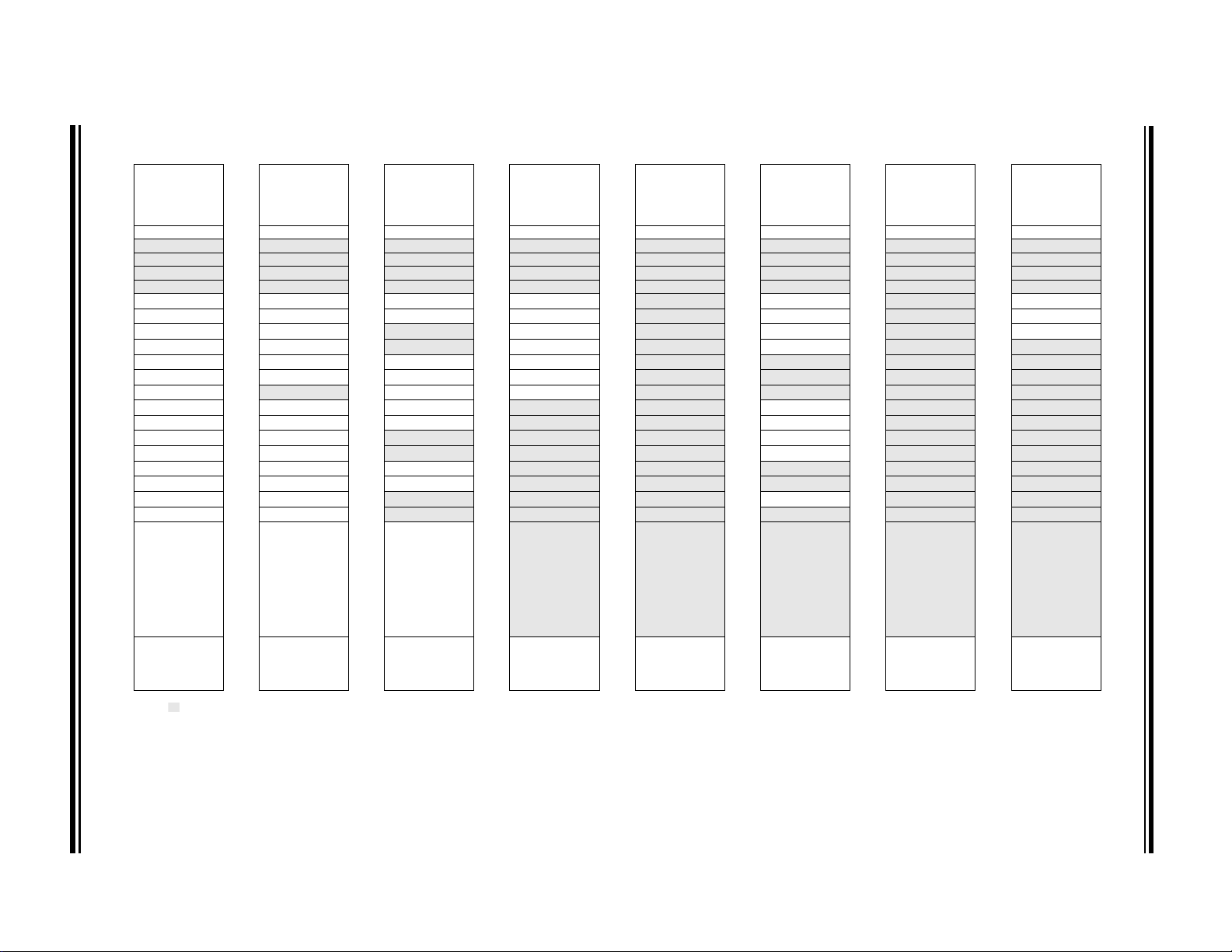
TABLE 3-6: PIC12(L)F1612/16(L)F1613 MEMORY MAP, BANK 24-31
PIC12(L)F1612/16(L)F1613
PIC12(L)F1612/16(L)F1613
Bank 27
D8Ch
SMT1TMRL
D8Dh
SMT1TMRH
D8Eh
SMT1TMRU
D8Fh
SMT1CPRL
D90h
SMT1CPRH
D91h
SMT1CPRU
D92h
SMT1CPWL
D93h
SMT1CPWH
D94h
SMT1CPWU
D95h
SMT1PRL
D96h
SMT1PRH
D97h
SMT1PRU
D98h
SMT1CON0
D99h
SMT1CON1
D9Ah
SMT1STAT
D9Bh
SMT1CLK
D9Ch
SMT1SIG
D9Dh
SMT1WIN
D9Eh
SMT2TMRL
D9Fh
SMT2TMRH
DA0h
SMT2TMRU
DA1h
SMT2CPRL
DA2h
SMT2CPRH
DA3h
SMT2CPRU
DA4h
SMT2CPWL
DA5h
SMT2CPWH
DA6h
SMT2CPWU
DA7h
SMT2PRL
DA8h
SMT2PRH
DA9h
SMT2PRU
DAAh
SMT2CON0
DABh
SMT2CON1
DACh
SMT2STAT
DADh
SMT2CLK
DAEh
SMT2SIG
DAFh
SMT2WIN
DB0h
—
DEFh
Legend: = Unimplemented data memory locations,
read as ‘0’.
Bank 31
F8Ch
FE3h
Unimplemented
Read as ‘0’
FE4h
STATUS_SHAD
FE5h
WREG_SHAD
FE6h
BSR_SHAD
FE7h
PCLATH_SHAD
FE8h
FSR0L_SHAD
FE9h
FSR0H_SHAD
FEAh
FSR1L_SHAD
FEBh
FSR1H_SHAD
FECh
—
FEDh
STKPTR
FEEh
TOSL
FEFh
TOSH
Legend: = Unimplemented data memory locations,
read as ‘0’.
TABLE 3-7: PIC12(L)F1612/16(L)F1613
MEMORY MAP, BANK 27
2014 Microchip Technology Inc. Preliminary DS40001737A-page 25
TABLE 3-8: PIC12(L)F1612/16(L)F1613
MEMORY MAP, BANK 31
PIC12(L)F1612/16(L)F1613
3.2.6 CORE FUNCTION REGISTERS SUMMARY
The Core Function registers listed in Ta bl e 3 -9 can be
addressed from any Bank.
TABLE 3-9: CORE FUNCTION REGISTERS SUMMARY
Addr Name Bit 7 Bit 6 Bit 5 Bit 4 Bit 3 Bit 2 Bit 1 Bit 0
Bank 0-31
x00h or
INDF0
x80h
x01h or
INDF1
x81h
x02h or
PCL Program Counter (PC) Least Significant Byte 0000 0000 0000 0000
x82h
x03h or
STATUS
x83h
x04h or
FSR0L Indirect Data Memory Address 0 Low Pointer 0000 0000 uuuu uuuu
x84h
x05h or
FSR0H Indirect Data Memory Address 0 High Pointer 0000 0000 0000 0000
x85h
x06h or
FSR1L Indirect Data Memory Address 1 Low Pointer 0000 0000 uuuu uuuu
x86h
x07h or
FSR1H Indirect Data Memory Address 1 High Pointer 0000 0000 0000 0000
x87h
x08h or
BSR
x88h
x09h or
WREG Working Register 0000 0000 uuuu uuuu
x89h
x0Ah or
PCLATH
x8Ah
x0Bh or
INTCON GIE PEIE TMR0IE INTE IOCIE TMR0IF INTF IOCIF 0000 0000 0000 0000
x8Bh
Legend: x = unknown, u = unchanged, q = value depends on condition, - = unimplemented, read as ‘0’, r = reserved.
Addressing this location uses contents of FSR0H/FSR0L to address data memory
(not a physical register)
Addressing this location uses contents of FSR1H/FSR1L to address data memory
(not a physical register)
— — —TOPD ZDCC---1 1000 ---q quuu
— — —BSR<4:0>---0 0000 ---0 0000
— Write Buffer for the upper 7 bits of the Program Counter -000 0000 -000 0000
Shaded locations are unimplemented, read as ‘0’.
Val ue o n
POR, BOR
xxxx xxxx uuuu uuuu
xxxx xxxx uuuu uuuu
Value on all
other Resets
DS40001737A-page 26 Preliminary 2014 Microchip Technology Inc.
2014 Microchip Technology Inc. Preliminary DS40001737A-page 27
TABLE 3-10: SPECIAL FUNCTION REGISTER SUMMARY
Addr Name Bit 7 Bit 6 Bit 5 Bit 4 Bit 3 Bit 2 Bit 1 Bit 0
Bank 0
00Ch PORTA
00Dh
00Eh PORTC
00Fh
010h
011h PIR1 TMR1GIF ADIF
012h PIR2
013h PIR3
014h PIR4 SCANIF CRCIF SMT2PWAIF SMT2PRAIF SMT2IF SMT1PWAIF SMT1PRAIF SMT1IF 0000 0000 0000 0000
015h TMR0 Holding Register for the 8-bit Timer0 Count xxxx xxxx uuuu uuuu
016h TMR1L Holding Register for the Least Significant Byte of the 16-bit TMR1 Count xxxx xxxx uuuu uuuu
017h TMR1H Holding Register for the Most Significant Byte of the 16-bit TMR1 Count xxxx xxxx uuuu uuuu
018h T1CON TMR1CS<1:0> T1CKPS<1:0>
019h T1GCON TMR1GE T1GPOL T1GTM T1GSPM T1GGO/
01Ah TMR2 Timer2 Module Register 0000 0000 0000 0000
01Bh PR2 Timer2 Period Register 1111 1111 1111 1111
01Ch T2CON ON CKPS<2:0> OUTPS<3:0> 0000 0000 0000 0000
01Dh T2HLT PSYNC CKPOL CKSYNC
01Eh T2CLKCON
01Fh T2RST
Legend: x = unknown, u = unchanged, q = value depends on condition, - = unimplemented, r = reserved. Shaded locations are unimplemented, read as ‘0’.
Note 1: PIC12F1612/16F1613 only.
— Unimplemented — —
(4)
— Unimplemented — —
— Unimplemented — —
2: Unimplemented, read as ‘1’.
3: PIC12(L)F1612 only.
4: PIC16(L)F1613 only.
— — RA5 RA4 RA3 RA2 RA1 RA0 --xx xxxx --xx xxxx
— — RC5 RC4 RC3 RC2 RC1 RC0 --xx xxxx --xx xxxx
—C2IF
— —CWGIFZCDIF — — — — --00 ---- --00 ----
— — — — — T2CS<2:0> ---- -000 ---- -000
— — — — RSEL<3:0> ---- 0000 ---- 0000
(4)
— — — CCP1IF TMR2IF TMR1IF 00-- -000 00-- -000
C1IF — — TMR6IF TMR4IF CCP2IF -00- -000 -00- -000
—T1SYNC—TMR1ON0000 -0-0 uuuu -u-u
T1GVAL T1GSS<1:0> 0000 0x00 uuuu uxuu
DONE
—MODE<3:0>000- 0000 000- 0000
Val ue o n
POR, BOR
Value on all
other Resets
PIC12(L)F1612/16(L)F1613
DS40001737A-page 28 Preliminary 2014 Microchip Technology Inc.
TABLE 3-10: SPECIAL FUNCTION REGISTER SUMMARY (CONTINUED)
Addr Name Bit 7 Bit 6 Bit 5 Bit 4 Bit 3 Bit 2 Bit 1 Bit 0
Bank 1
08Ch TRISA
08Dh
08Eh TRISC
08Fh
090h
091h PIE1 TMR1GIE ADIE
092h PIE2
093h PIE3
094h PIE4 SCANIE CRCIE SMT2PWAIE SMT2PRAIE SMT2IE SMT1PWAIE SMT1PRAIE SMT1IE 0000 0000 0000 0000
095h OPTION_REG WPUEN
096h PCON STKOVF STKUNF WDTWV
097h
098h OSCTUNE
099h OSCCON SPLLEN IRCF<3:0>
09Ah OSCSTAT
09Bh ADRESL ADC Result Register Low xxxx xxxx uuuu uuuu
09Ch ADRESH ADC Result Register High xxxx xxxx uuuu uuuu
09Dh ADCON0
09Eh ADCON1 ADFM ADCS<2:0>
09Fh ADCON2 TRIGSEL<3:0>
Legend: x = unknown, u = unchanged, q = value depends on condition, - = unimplemented, r = reserved. Shaded locations are unimplemented, read as ‘0’.
Note 1: PIC12F1612/16F1613 only.
— Unimplemented — —
(4)
— Unimplemented — —
— Unimplemented — —
— Unimplemented — —
2: Unimplemented, read as ‘1’.
3: PIC12(L)F1612 only.
4: PIC16(L)F1613 only.
— — TRISA5 TRISA4 —
— — TRISC5 TRISC4 TRISC3 TRISC2 TRISC1 TRISC0 --11 1111 --11 1111
—C2IE
— — CWGIE ZCDIE — — — — --00 ---- --00 ----
— — TUN<5:0> --00 0000 --00 0000
— PLLR — HFIOFR HFIOFL MFIOFR LFIOFR HFIOFS -0-0 0000 -q-q qqqq
— CHS<4:0> GO/DONE ADON -000 0000 -000 0000
(4)
INTEDG TMR0CS TMR0SE PSA PS<2:0> 1111 1111 1111 1111
— — — CCP1IE TMR2IE TMR1IE 00-- -000 00-- -000
C1IE — — TMR6IE TMR4IE CCP2IE -00- -000 -00- -000
RWDT RMCLR RI POR BOR 00-1 11qq qq-q qquu
(2)
— — ADPREF<1:0> 0000 --00 0000 --00
— — — — 0000 ---- 0000 ----
TRISA2 TRISA1 TRISA0 --11 1111 --11 1111
—SCS<1:0>0011 1-00 0011 1-00
Val ue o n
POR, BOR
Value on all
other Resets
PIC12(L)F1612/16(L)F1613
2014 Microchip Technology Inc. Preliminary DS40001737A-page 29
TABLE 3-10: SPECIAL FUNCTION REGISTER SUMMARY (CONTINUED)
Addr Name Bit 7 Bit 6 Bit 5 Bit 4 Bit 3 Bit 2 Bit 1 Bit 0
Bank 2
10Ch LATA
10Dh
10Eh LATC
10Fh
110h
111h CM1CON0 C1ON C1OUT C1OE C1POL
112h CM1CON1 C1INTP C1INTN C1PCH<1:0>
113h CM2CON0
114h CM2CON1
115h CMOUT
116h BORCON SBOREN BORFS
117h FVRCON FVREN FVRRDY TSEN TSRNG CDAFVR<1:0> ADFVR<1:0> 0q00 0000 0q00 0000
118h DAC1CON0 DAC1EN
119h DAC1CON1 DAC1R<7:0> 0000 0000 0000 0000
11Ah
11Bh
11Ch ZCD1CON ZCD1EN ZCD1OE ZCD1OUT ZCD1POL
11Dh APFC ON
11Eh
11Fh
Legend: x = unknown, u = unchanged, q = value depends on condition, - = unimplemented, r = reserved. Shaded locations are unimplemented, read as ‘0’.
Note 1: PIC12F1612/16F1613 only.
— Unimplemented — —
(4)
— Unimplemented — —
— Unimplemented — —
(4)
(4)
— Unimplemented — —
— Unimplemented — —
— Unimplemented — —
— Unimplemented — —
2: Unimplemented, read as ‘1’.
3: PIC12(L)F1612 only.
4: PIC16(L)F1613 only.
— —LATA5LATA4— LATA2 LATA1 LATA0 --xx -xxx --uu -uuu
— — LAT C5 LATC4 LATC3 LAT C2 LATC1 LAT C0 --xx xxxx --uu uuuu
— C1SP C1HYS C1SYNC 0000 -100 0000 -100
— C1NCH<2:0> 0000 -000 0000 -000
C2ON C2OUT C2OE C2POL — C2SP C2HYS C2SYNC 0000 -100 0000 -100
C2INTP C2INTN C2PCH<1:0> — C2NCH<2:0> 0000 -000 0000 -000
— — — — — — MC2OUT MC1OUT ---- --00 ---- --00
— — — — — BORRDY 10-- ---q uu-- ---u
—DAC1OE1— DAC1PSS<1:0> — — 0-0- 00-- 0-0- 00--
— — ZCD1INTP ZCD1INTN 0000 --00 0000 --00
(4)
CCP1SEL
— CWGASEL
(3)
CWGBSEL
(3)
—T1GSEL— CCP2SEL
Val ue o n
POR, BOR
(3)
-00- 0-00 -00- 0-00
Value on all
other Resets
PIC12(L)F1612/16(L)F1613
DS40001737A-page 30 Preliminary 2014 Microchip Technology Inc.
TABLE 3-10: SPECIAL FUNCTION REGISTER SUMMARY (CONTINUED)
Addr Name Bit 7 Bit 6 Bit 5 Bit 4 Bit 3 Bit 2 Bit 1 Bit 0
Bank 3
18Ch ANSELA
18Dh
18Eh ANSELC
18Fh
190h
191h PMADRL Flash Program Memory Address Register Low Byte 0000 0000 0000 0000
192h PMADRH
193h PMDATL Flash Program Memory Read Data Register Low Byte xxxx xxxx uuuu uuuu
194h PMDATH
195h PMCON1
196h PMCON2 Flash Program Memory Control Register 2 0000 0000 0000 0000
197h VREGCON
Bank 4
20Ch WPUA
20Dh
20Eh WPUC
Legend: x = unknown, u = unchanged, q = value depends on condition, - = unimplemented, r = reserved. Shaded locations are unimplemented, read as ‘0’.
Note 1: PIC12F1612/16F1613 only.
— Unimplemented — —
— Unimplemented — —
— Unimplemented — —
198h
— Unimplemented — —
to
19Fh
— Unimplemented — —
20Fh
— Unimplemented — —
to
21Fh
2: Unimplemented, read as ‘1’.
3: PIC12(L)F1612 only.
4: PIC16(L)F1613 only.
(4)
(1)
(4)
— — —ANSA4— ANSA2 ANSA1 ANSA0 ---1 -111 ---1 -111
— — — — ANSC3 ANSC2 ANSC1 ANSC0 ---- 1111 ---- 1111
(2)
—
— — Flash Program Memory Read Data Register High Byte --xx xxxx --uu uuuu
(2)
—
— — — — — —VREGPMReserved ---- --01 ---- --01
— — WPUA5 WPUA4 WPUA3 WPUA2 WPUA1 WPUA0 --11 1111 --11 1111
— — WPUC5 WPUC4 WPUC3 WPUC2 WPUC1 WPUC0 --11 1111 --11 1111
Flash Program Memory Address Register High Byte 1000 0000 1000 0000
CFGS LWLO FREE WRERR WREN WR RD 1000 x000 1000 q000
Val ue o n
POR, BOR
Value on all
other Resets
PIC12(L)F1612/16(L)F1613
 Loading...