

Page 1

PIC12LF1552
8-Pin Flash, 8-Bit Microcontrollers
High-Performance RISC CPU:
• C Compiler Optimized Architecture
• Only 49 Instructions
• 2K Words Linear Program Memory Addressing
• 256 bytes Linear Data Memory Addressing
• Operating Speed:
- DC – 32 MHz clock input
- DC – 125 ns instruction cycle
• Interrupt Capability with Automatic Context
Saving
• 16-Level Deep Hardware Stack with Optional
Overflow/Underflow Reset
• Direct, Indirect and Relative Addressing modes:
- Two full 16-bit File Select Registers (FSRs)
- FSRs can read program and data memory
Flexible Oscillator Structure:
• 16 MHz Internal Oscillator Block:
- Factory calibrated to ±1%, typical
- Software selectable frequency range from
32 MHz to 31 kHz
• 4x Phase-Lock Loop (PLL), usable with 16 MHz
internal oscillator
- Allows 32 MHz software selectable clock
frequency
• 31 kHz Low-Power Internal Oscillator
• Three External Clock modes up to 20 MHz
Special Microcontroller Features:
• Operating Voltage Range:
- 1.8V to 3.6V
• Self-Programmable under Software Control
• Power-on Reset (POR)
• Power-up Timer (PWRT)
• Programmable Low-Power Brown-Out Reset
(LPBOR)
• Extended Watchdog Timer (WDT):
- Programmable period from 1 ms to 256s
• Programmable Code Protection
• In-Circuit Serial Programming™ (ICSP™) via Two
Pins
• Enhanced Low-Voltage Programming (LVP)
• Power-Saving Sleep mode:
- Low-Power Sleep mode
- Low-Power BOR (LPBOR)
• Integrated Temperature Indicator
• 128 Bytes High-Endurance Flash:
- 100,000 write Flash endurance (minimum)
Low-Power Features:
• Standby Current:
- 20 nA @ 1.8V, typical
• Watchdog Timer Current:
- 200 nA @ 1.8V, typical
• Operating Current:
-30 A/MHz @ 1.8V, typical
Peripheral Features:
• Analog-to-Digital Converter (ADC):
- 10-bit resolution
- 5 external channels
- 2 internal channels:
- Fixed Voltage Reference
- Temperature Indicator channel
- Auto acquisition capability
- Conversion available during Sleep
- Special Event Triggers
• Hardware Capacitive Voltage Divider (CVD)
- Double sample conversions
- Two sets of result registers
- Inverted acquisition
- 7-bit pre-charge timer
- 7-bit acquisition timer
- Two guard ring output drives
- Adjustable sample and hold capacitor array
• Voltage Reference module:
- Fixed Voltage Reference (FVR) with 1.024V
and 2.048V output levels
• 6 I/O Pins (1 Input-only Pin):
- High current sink/source 25 mA/25 mA
- Individually programmable weak pull-ups
- Individually programmable interrupt-on-change
(IOC) pins
• Timer0: 8-Bit Timer/Counter with 8-Bit
Programmable Prescaler
• Master Synchronous Serial Port (MSSP) with SPI
2
CTM with:
and I
- 7-bit address masking
- SMBus/PMBusTM compatibility
2012-2014 Microchip Technology Inc. DS40001674D-page 1
Page 2

PIC12LF1552
PIC12LF1552 Family Types Table
Device
(bytes)
Data SRAM
Data Sheet Index
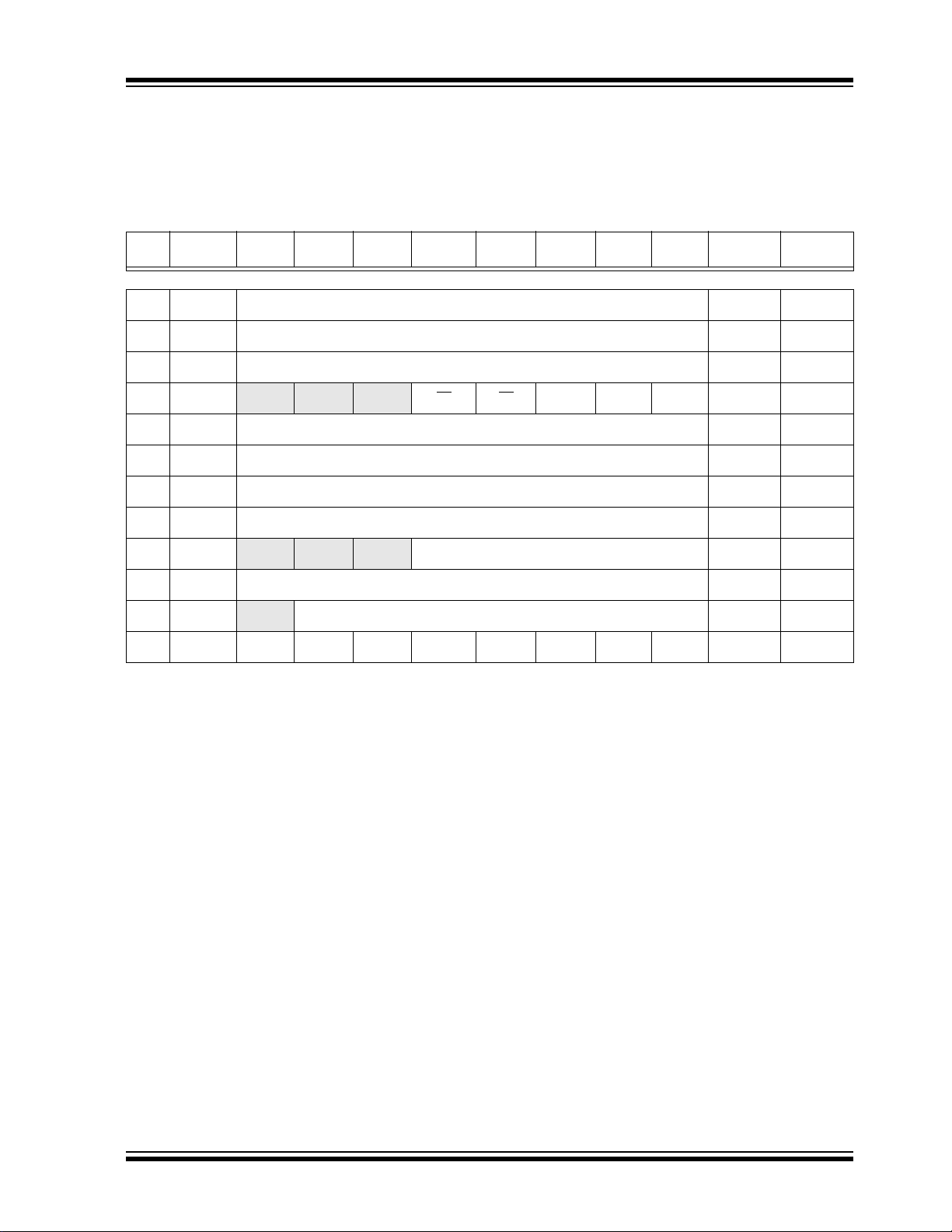
PIC12LF1552 (1) 2048 256 6 5 1 1 N/A
Note 1: Not available.
2: One pin is input-only.
Data Sheet Index: (Unshaded devices are described in this document.)
1: DS40001674 PIC12LF1552 Data Sheet, 8-Pin Flash, 8-bit Microcontrollers.
Note: For other small form-factor package availability and marking information, please visit
http://www.microchip.com/packaging or contact your local sales office.
Program Memory
Flash (words)
(2)
I/O’s
10-bit ADC (ch)
(8-bit)
Timers
C™/SPI)
2
MSSP (I
(1)
Debug
DS40001674D-page 2 2012-2014 Microchip Technology Inc.
Page 3

FIGURE 1: 8-PIN PDIP, SOIC, MSOP, UDFN
Note: See Ta b le 1 for location of all peripheral functions.
1
2
3
4
8
7
6
5
VDD
RA5
RA4
MCLR/VPP/RA3
V
SS
RA0/ICSPDAT
RA1/ICSPCLK
RA2
PIC12LF1552
TABLE 1: 8-PIN ALLOCATION TABLE
PIC12LF1552
I/O
Reference
ADC/Hardware CVD
8-Pin PDIP/SOIC/MSOP/UDFN
RA0 7 AN0 — — SDO
RA1 6 AN1 VREF+ — SCK
RA2 5 AN2
ADOUT
RA3 4 — — — SS
RA4 3 AN3
ADGRDA
RA5 2 AN4
ADGRDB
VDD 1 — — — — — — VDD
VSS 8— — — — —— VSS
Note 1: Default location for peripheral pin function. Alternate location can be selected using the APFCON register.
2: Alternate location for peripheral pin function selected by the APFCON register.
— T0CKI SDI
— — SDO
— — — IOC Y CLKIN
Timer
SS
SCL
SDA
SDA
SDI
(2)
(1)
MSSP
(1)
(1)
(1)
(2)
(2)
(2)
Interrupt
IOC Y ICSPDAT
IOC Y ICSPCLK
INT
IOC
IOC Y MCLR
IOC Y CLKOUT
Pull-Up
Y —
VPP
Basic
2012-2014 Microchip Technology Inc. DS40001674D-page 3
Page 4

PIC12LF1552
Table of Contents
1.0 Device Overview .......................................................................................................................................................................... 5
2.0 Enhanced Mid-Range CPU .......................................................................................................................................................... 8
3.0 Memory Organization ................................................................................................................................................................. 10
4.0 Device Configuration.................................................................................................................................................................. 31
5.0 Oscillator Module........................................................................................................................................................................ 36
6.0 Resets ........................................................................................................................................................................................ 44
7.0 Interrupts .................................................................................................................................................................................... 52
8.0 Power-down Mode (Sleep) ......................................................................................................................................................... 63
9.0 Watchdog Timer (WDT) ............................................................................................................................................................. 65
10.0 Flash Program Memory Control ................................................................................................................................................. 69
11.0 I/O Ports ..................................................................................................................................................................................... 85
12.0 Interrupt-on-Change ................................................................................................................................................................... 91
13.0 Fixed Voltage Reference (FVR) ................................................................................................................................................. 95
14.0 Temperature Indicator Module ................................................................................................................................................... 97
15.0 Analog-to-Digital Converter (ADC) Module ................................................................................................................................ 99
16.0 Hardware Capacitive Voltage Divider (CVD) Module ............................................................................................................... 112
17.0 Timer0 Module ......................................................................................................................................................................... 131
18.0 Master Synchronous Serial Port Module.................................................................................................................................. 134
19.0 In-Circuit Serial Programming™ (ICSP™) ............................................................................................................................... 186
20.0 Instruction Set Summary .......................................................................................................................................................... 188
21.0 Electrical Specifications............................................................................................................................................................ 202
22.0 DC and AC Characteristics Graphs and Charts ....................................................................................................................... 219
23.0 Development Support............................................................................................................................................................... 234
24.0 Packaging Information.............................................................................................................................................................. 238
The Microchip Web Site..................................................................................................................................................................... 251
Customer Change Notification Service .............................................................................................................................................. 251
Customer Support .............................................................................................................................................................................. 251
Product Identification System............................................................................................................................................................. 252
TO OUR VALUED CUSTOMERS
It is our intention to provide our valued customers with the best documentation possible to ensure successful use of your Microchip
products. To this end, we will continue to improve our publications to better suit your needs. Our publications will be refined and
enhanced as new volumes and updates are introduced.
If you have any questions or comments regarding this publication, please contact the Marketing Communications Department via
E-mail at docerrors@microchip.com. We welcome your feedback.
Most Current Data Sheet
To obtain the most up-to-date version of this data sheet, please register at our Worldwide Web site at:
http://www.microchip.com
You can determine the version of a data sheet by examining its literature number found on the bottom outside corner of any page.
The last character of the literature number is the version number, (e.g., DS30000000A is version A of document DS30000000).
Errata
An errata sheet, describing minor operational differences from the data sheet and recommended workarounds, may exist for current
devices. As device/documentation issues become known to us, we will publish an errata sheet. The errata will specify the revision
of silicon and revision of document to which it applies.
To determine if an errata sheet exists for a particular device, please check with one of the following:
• Microchip’s Worldwide Web site; http://www.microchip.com
• Your local Microchip sales office (see last page)
When contacting a sales office, please specify which device, revision of silicon and data sheet (include literature number) you are
using.
Customer Notification System
Register on our web site at www.microchip.com to receive the most current information on all of our products.
DS40001674D-page 4 2012-2014 Microchip Technology Inc.
Page 5

1.0 DEVICE OVERVIEW
The PIC12LF1552 are described within this data sheet.
They are available in 8-pin packages. Figure 1-1 shows a
block diagram of the PIC12LF1552 devices. Ta b l e 1 -2
shows the pinout descriptions.
Reference Ta bl e 1- 1 for peripherals available per
device.
TABLE 1-1: DEVICE PERIPHERAL
SUMMARY
Peripheral
PIC12LF1552
Analog-to-Digital Converter (ADC) ●
Hardware Capacitor Voltage Divider (CVD) ●
Fixed Voltage Reference (FVR) ●
Temperature Indicator ●
Master Synchronous Serial Ports
MSSP1 ●
Timers
Timer0 ●
PIC12LF1552
2012-2014 Microchip Technology Inc. DS40001674D-page 5
Page 6

PIC12LF1552
Note 1: See applicable chapters for more information on peripherals.
2: See Table 1-1 for peripherals available on specific devices.
CPU
Program
Flash Memory
RAM
Timing
Generation
INTRC
Oscillator
MCLR
(Figure 2-1)
Timer0
PORTA
ADC
10-Bit
FVR
Te mp .
Indicator
CLKIN
CLKOUT
MSSP
Hardware
CVD
FIGURE 1-1: PIC12LF1552 BLOCK DIAGRAM
DS40001674D-page 6 2012-2014 Microchip Technology Inc.
Page 7

PIC12LF1552
TABLE 1-2: PIC12LF1552 PINOUT DESCRIPTION
Input
Name Function
(1)
RA0/AN0/SDO
ICSPDAT
/SS
(2)
/
RA0 TTL CMOS General purpose I/O.
AN0 AN — ADC Channel input.
SDO — CMOS SPI data output.
SS
ICSPDAT ST CMOS ICSP™ Data I/O.
RA1/AN1/V
ICSPCLK
REF+/SCK/SCL/
RA1 TTL CMOS General purpose I/O.
AN1 AN — ADC Channel input.
REF+ AN — ADC Positive Voltage Reference input.
V
SCK ST CMOS SPI clock.
SCL I
ICSPCLK ST — ICSP™ Programming Clock.
RA2/AN2/ADOUT/T0CKI/
(1)
(1)
/SDA
SDI
/INT
RA2 ST CMOS General purpose I/O.
AN2 AN — ADC Channel input.
ADOUT CMOS — ADC with CVD output.
T0CKI ST — Timer0 clock input.
SDI ST — SPI data input.
SDA I
INT ST — External interrupt.
(1)
RA3/MCLR/
(2)
SDA
VPP/SS
/SDI
(2)
/
RA3 TTL — General purpose input.
MCLR
V
PP HV — Programming voltage.
SS
SDI ST — SPI data input.
SDA I
RA4/AN3/SDO
ADGRDA
/CLKOUT/
RA4 TTL CMOS General purpose I/O.
AN3 AN — ADC Channel input.
(2)
SDO — CMOS SPI data output.
CLKOUT — CMOS F
ADGRDA — CMOS Guard ring output A.
RA5/AN4/CLKIN/ADGRDB RA5 TTL CMOS General purpose I/O.
AN4 AN — ADC Channel input.
CLKIN CMOS — External clock input (EC mode).
ADGRDB — CMOS Guard ring output B.
DD VDD Power — Positive supply.
V
SS VSS Power — Ground reference.
V
Legend: AN = Analog input or output CMOS= CMOS compatible input or output OD = Open Drain
TTL = TTL compatible input ST = Schmitt Trigger input with CMOS levels I
HV = High Voltage XTAL = Crystal levels
Note 1: Default location for peripheral pin function. Alternate location can be selected using the APFCON register.
2: Alternate location for peripheral pin function selected by the APFCON register.
Typ e
Output
Typ e
Description
ST — Slave Select input.
2
CODI2C™ clock.
2
CODI2C™ data input/output.
ST — Master Clear with internal pull-up.
ST — Slave Select input.
2
CODI2C™ data input/output.
OSC/4 output.
2
C™ = Schmitt Trigger input with I2C
2012-2014 Microchip Technology Inc. DS40001674D-page 7
Page 8

PIC12LF1552
Data Bus
8
14
Program
Bus
Instruction reg
Program Counter
8 Level Stack
(13-bit)
Direct Addr
7
12
Addr MUX
FSR reg
STATUS reg
MUX
ALU
Instruction
Decode &
Control
Timing
Generation
CLKIN
CLKOUT
8
8
12
3
Internal
Oscillator
Block
Configuration
Data Bus
8
14
Program
Bus
Instruction reg
Program Counter
8 Level Stack
(13-bit)
Direct Addr
7
Addr MUX
FSR reg
STATUS reg
MUX
ALU
W Reg
Instruction
Decode &
Control
Timing
Generation
8
8
3
Internal
Oscillator
Block
Configuration
15
Data Bus
8
14
Program
Bus
Instruction Reg
Program Counter
16-Level Stack
(15-bit)
Direct Addr
7
RAM Addr
Addr MUX
Indirect
Addr
FSR0 Reg
STATUS Reg
MUX
ALU
Instruction
Decode and
Control
Timing
Generation
8
8
3
Internal
Oscillator
Block
Configuration
Flash
Program
Memory
RAM
FSR regFSR reg
FSR1 Reg
15
15
MUX
15
Program Memory
Read (PMR)
12
FSR regFSR reg
BSR Reg
5
Power-up
Timer
Power-on
Reset
Watchdog
Timer
V
DD
Brown-out
Reset
VSSVDD VSSVDD VSS
2.0 ENHANCED MID-RANGE CPU
This family of devices contain an enhanced mid-range
8-bit CPU core. The CPU has 49 instructions. Interrupt
capability includes automatic context saving. The
hardware stack is 16 levels deep and has Overflow and
Underflow Reset capability. Direct, Indirect, and
Relative addressing modes are available. Two File
Select Registers (FSRs) provide the ability to read
program and data memory.
FIGURE 2-1: CORE BLOCK DIAGRAM
• Automatic Interrupt Context Saving
• 16-level Stack with Overflow and Underflow
• File Select Registers
• Instruction Set
DS40001674D-page 8 2012-2014 Microchip Technology Inc.
Page 9

2.1 Automatic Interrupt Context Saving
During interrupts, certain registers are automatically
saved in shadow registers and restored when returning
from the interrupt. This saves stack space and user
code. See Section 7.5 “Automatic Context Saving”,
for more information.
2.2 16-Level Stack with Overflow and Underflow
These devices have an external stack memory 15 bits
wide and 16 words deep. A Stack Overflow or
Underflow will set the appropriate bit (STKOVF or
STKUNF) in the PCON register and, if enabled, will
cause a software Reset. See section Section 3.5
“Stack” for more details.
2.3 File Select Registers
There are two 16-bit File Select Registers (FSR). FSRs
can access all file registers and program memory,
which allows one Data Pointer for all memory. When an
FSR points to program memory, there is one additional
instruction cycle in instructions using INDF to allow the
data to be fetched. General purpose memory can now
also be addressed linearly, providing the ability to
access contiguous data larger than 80 bytes. There are
also new instructions to support the FSRs. See
Section 3.6 “Indirect Addressing” for more details.
PIC12LF1552
2.4 Instruction Set
There are 49 instructions for the enhanced mid-range
CPU to support the features of the CPU. See
Section 20.0 “Instruction Set Summary” for more
details.
2012-2014 Microchip Technology Inc. DS40001674D-page 9
Page 10

PIC12LF1552
3.0 MEMORY ORGANIZATION
These devices contain the following types of memory:
• Program Memory
- Configuration Words
-Device ID
-User ID
- Flash Program Memory
• Data Memory
- Core Registers
- Special Function Registers
- General Purpose RAM
- Common RAM
The following features are associated with access and
control of program memory and data memory:
• PCL and PCLATH
•Stack
• Indirect Addressing
3.1 Program Memory Organization
The enhanced mid-range core has a 15-bit program
counter capable of addressing a 32K x 14 program
memory space. Table 3-1 shows the memory sizes
implemented. Accessing a location above these
boundaries will cause a wrap-around within the
implemented memory space. The Reset vector is at
0000h and the interrupt vector is at 0004h (see
Figure 3-1).
TABLE 3-1: DEVICE SIZES AND ADDRESSES
Device
PIC12LF1552 2,048 07FFh 0780h-07FFh
Note 1: High-endurance Flash applies to the low byte of each address in the range.
Program Memory
Space (Words)
Last Program Memory
Address
High-Endurance Flash
Memory Address Range
(1)
DS40001674D-page 10 2012-2014 Microchip Technology Inc.
Page 11

PIC12LF1552
PC<14:0>
15
0000h
0004h
Stack Level 0
Stack Level 15
Reset Vector
Interrupt Vector
Stack Level 1
0005h
On-chip
Program
Memory
Page 0
7FFFh
Wraps to Page 0
Wraps to Page 0
Wraps to Page 0
0800h
CALL, CALLW
RETURN, RETLW
Interrupt, RETFIE
Rollover to Page 0
Rollover to Page 0
7FFFh
constants
BRW ;Add Index in W to
;program counter to
;select data
RETLW DATA0 ;Index0 data
RETLW DATA1 ;Index1 data
RETLW DATA2
RETLW DATA3
my_function
;… LOTS OF CODE…
MOVLW DATA_INDEX
call constants
;… THE CONSTANT IS IN W
FIGURE 3-1: PROGRAM MEMORY MAP
AND STACK FOR
PIC12LF1552
3.1.1 READING PROGRAM MEMORY AS DATA
There are two methods of accessing constants in
program memory. The first method is to use tables of
RETLW instructions. The second method is to set an
FSR to point to the program memory.
3.1.1.1 RETLW Instruction
The RETLW instruction can be used to provide access
to tables of constants. The recommended way to create
such a table is shown in Example 3-1.
EXAMPLE 3-1: RETLW INSTRUCTION
The BRW instruction makes this type of table very
simple to implement. If your code must remain portable
with previous generations of microcontrollers, then the
BRW instruction is not available so the older table read
method must be used.
2012-2014 Microchip Technology Inc. DS40001674D-page 11
Page 12

PIC12LF1552
constants
RETLW DATA0 ;Index0 data
RETLW DATA1 ;Index1 data
RETLW DATA2
RETLW DATA3
my_function
;… LOTS OF CODE…
MOVLW LOW constants
MOVWF FSR1L
MOVLW HIGH constants
MOVWF FSR1H
MOVIW 0[FSR1]
;THE PROGRAM MEMORY IS IN W
Addresses BANKx
x00h or x80h INDF0
x01h or x81h INDF1
x02h or x82h PCL
x03h or x83h STATUS
x04h or x84h FSR0L
x05h or x85h FSR0H
x06h or x86h FSR1L
x07h or x87h FSR1H
x08h or x88h BSR
x09h or x89h WREG
x0Ah or x8Ah PCLATH
x0Bh or x8Bh INTCON
3.1.1.2 Indirect Read with FSR
The program memory can be accessed as data by
setting bit 7 of the FSRxH register and reading the
matching INDFx register. The MOVIW instruction will
place the lower eight bits of the addressed word in the
W register. Writes to the program memory cannot be
performed via the INDF registers. Instructions that
access the program memory via the FSR require one
extra instruction cycle to complete. Example 3-2
demonstrates accessing the program memory via an
FSR.
The High directive will set bit<7> if a label points to a
location in program memory.
EXAMPLE 3-2: ACCESSING PROGRAM
MEMORY VIA FSR
3.2.1 CORE REGISTERS
The core registers contain the registers that directly
affect the basic operation. The core registers occupy
the first 12 addresses of every data memory bank
(addresses x00h/x08h through x0Bh/x8Bh). These
registers are listed below in Ta b le 3 - 2 . For detailed
information, see Tab le 3 -5 .
TABLE 3-2: CORE REGISTERS
3.2 Data Memory Organization
The data memory is partitioned into 32 memory banks
with 128 bytes in a bank. Each bank consists of
(Figure 3-2):
• 12 core registers
• 20 Special Function Registers (SFR)
• Up to 80 bytes of General Purpose RAM (GPR)
• 16 bytes of common RAM
The active bank is selected by writing the bank number
into the Bank Select Register (BSR). Unimplemented
memory will read as ‘0’. All data memory can be
accessed either directly (via instructions that use the
file registers) or indirectly via the two File Select
Registers (FSR). See Section 3.6 “Indirect
Addressing” for more information.
Data memory uses a 12-bit address. The upper seven
bits of the address define the Bank address and the
lower five bits select the registers/RAM in that bank.
DS40001674D-page 12 2012-2014 Microchip Technology Inc.
Page 13

PIC12LF1552
3.2.1.1 STATUS Register
The STATUS register, shown in Register 3-1, contains:
• the arithmetic status of the ALU
• the Reset status
The STATUS register can be the destination for any
instruction, like any other register. If the STATUS
register is the destination for an instruction that affects
the Z, DC or C bits, then the write to these three bits is
disabled. These bits are set or cleared according to the
device logic. Furthermore, the TO
writable. Therefore, the result of an instruction with the
STATUS register as destination may be different than
intended.
and PD bits are not
For example, CLRF STATUS will clear the upper three
bits and set the Z bit. This leaves the STATUS register
as ‘000u u1uu’ (where u = unchanged).
It is recommended, therefore, that only BCF, BSF,
SWAPF and MOVWF instructions are used to alter the
STATUS register, because these instructions do not
affect any Status bits. For other instructions not
affecting any Status bits (Refer to Section 20.0
“Instruction Set Summary”).
Note 1: The C and DC bits operate as Borrow
and Digit Borrow out bits, respectively, in
subtraction.
3.3 Register Definitions: Status
REGISTER 3-1: STATUS: STATUS REGISTER
U-0 U-0 U-0 R-1/q R-1/q R/W-0/u R/W-0/u R/W-0/u
— — —
bit 7 bit 0
Legend:
R = Readable bit W = Writable bit U = Unimplemented bit, read as ‘0’
u = Bit is unchanged x = Bit is unknown -n/n = Value at POR and BOR/Value at all other Resets
‘1’ = Bit is set ‘0’ = Bit is cleared q = Value depends on condition
TO
PD ZDC
(1)
(1)
C
bit 7-5 Unimplemented: Read as ‘0’
bit 4 TO
bit 3 PD
bit 2 Z: Zero bit
bit 1 DC: Digit Carry/Digit Borrow
bit 0 C: Carry/Borrow
Note 1: For Borrow
second operand. For rotate (RRF, RLF) instructions, this bit is loaded with either the high-order or low-order
bit of the source register.
: Time-Out bit
1 = After power-up, CLRWDT instruction or SLEEP instruction
0 = A WDT time-out occurred
: Power-Down bit
1 = After power-up or by the CLRWDT instruction
0 = By execution of the SLEEP instruction
1 = The result of an arithmetic or logic operation is zero
0 = The result of an arithmetic or logic operation is not zero
1 = A carry-out from the 4th low-order bit of the result occurred
0 = No carry-out from the 4th low-order bit of the result
(1)
bit
(ADDWF, ADDLW, SUBLW, SUBWF instructions)
1 = A carry-out from the Most Significant bit of the result occurred
0 = No carry-out from the Most Significant bit of the result occurred
, the polarity is reversed. A subtraction is executed by adding the two’s complement of the
bit (ADDWF, ADDLW, SUBLW, SUBWF instructions)
(1)
(1)
2012-2014 Microchip Technology Inc. DS40001674D-page 13
Page 14

PIC12LF1552
0Bh
0Ch
1Fh
20h
6Fh
70h
7Fh
00h
Common RAM
(16 bytes)
General Purpose RAM
(80 bytes maximum)
Core Registers
(12 bytes)
Special Function Registers
(20 bytes maximum)
Memory Region
7-bit Bank Offset
3.3.1 SPECIAL FUNCTION REGISTER
The Special Function Registers are registers used by
the application to control the desired operation of
peripheral functions in the device. The Special Function
Registers occupy the 20 bytes after the core registers of
every data memory bank (addresses x0Ch/x8Ch
through x1Fh/x9Fh). The registers associated with the
operation of the peripherals are described in the
appropriate peripheral chapter of this data sheet.
3.3.2 GENERAL PURPOSE RAM
There are up to 80 bytes of GPR in each data memory
bank. The Special Function Registers occupy the 20
bytes after the core registers of every data memory
bank (addresses x0Ch/x8Ch through x1Fh/x9Fh).
3.3.2.1 Linear Access to GPR
The general purpose RAM can be accessed in a
non-banked method via the FSRs. This can simplify
access to large memory structures. See Section 3.6.2
“Linear Data Memory” for more information.
3.3.3 COMMON RAM
There are 16 bytes of common RAM accessible from all
banks.
FIGURE 3-2: BANKED MEMORY
PARTITIONING
DS40001674D-page 14 2012-2014 Microchip Technology Inc.
3.3.4 DEVICE MEMORY MAPS
The memory maps for PIC12LF1552 are as shown in
Table 3-3.
Page 15

2012-2014 Microchip Technology Inc. DS40001674D-page 15
TABLE 3-3: PIC12LF1552 MEMORY MAP
BANK 0 BANK 1 BANK 2 BANK 3 BANK 4 BANK 5 BANK 6 BANK 7
000h
Core Registers
(Ta bl e 3- 2 )
00Bh 08Bh 10Bh 18Bh 20Bh 28Bh 30Bh 38Bh
00Ch PORTA 08Ch TRISA 10Ch LATA 18Ch ANSELA 20Ch WPUA 28Ch
00Dh
00Eh
00Fh
010h
011h PIR1 091h PIE1 111h
012h PIR2 092h PIE2 112h
013h
014h
015h TMR0 095h OPTION_REG 115h
016h
017h
018h
019h
01Ah
01Bh
01Ch
01Dh
01Eh
01Fh
020h
— 08Dh — 10Dh — 18Dh — 20Dh — 28Dh — 30Dh — 38Dh —
—08Eh—10Eh—18Eh—20Eh—28Eh—30Eh—38Eh—
—08Fh—10Fh—18Fh—20Fh—28Fh—30Fh—38Fh—
—090h—110h—190h—210h—290h
—093h—113h— 193h PMDATL 213h
—094h—114h— 194h PMDATH 214h
—
—
—
—
—
—
—
— 09Dh ADCON0
—
—
080h
Core Registers
(Ta bl e 3- 2 )
096h PCON 116h BORCON 196h PMCON2 216h
097h WDTCON 117h FVRCON 197h
098h
099h OSCCON 119h
09Ah OSCSTAT 11Ah
09Bh ADRESL
09Ch ADRESH
09Eh ADCON1
09Fh ADCON2
0A0h
—118h
100h
Core Registers
(Table 3-2)
— 191h PMADRL 211h
— 192h PMADRH 212h
— 195h PMCON1 215h
—
—
(1)
11Bh —19Bh
(1)
11Ch — 19Ch
(1)
11Dh APFCON 19Dh
(1)
11Eh
(1)
11Fh —19Fh
120h
—19Ah
—
180h
198h
199h
19Eh
1A0h
Core Registers
(Table 3-2)
—217h
—218h
—
—
—
—
—
—
—
200h
219h
21Ah
21Bh
21Ch
21Dh
21Eh
21Fh
220h
Core Registers
(Table 3-2)
SSPBUF
SSPADD
SSPMSK
SSPSTAT
SSPCON1
SSPCON2
SSPCON3
—
—299h— 319h — 399h —
—29Ah—31Ah—39Ah—
—29Bh—31Bh
— 29Ch — 31Ch
—
—
—
280h
Core Registers
(Table 3-2)
— 30Ch — 38Ch —
—
291h
292h
293h
294h
295h
296h
297h — 317h — 397h —
298h
29Dh
29Eh
29Fh
2A0h
—
—
—
—
—
— 316h — 396h
— 318h — 398h —
—
—
—
300h
310h
311h
312h
313h
314h
315h
31Dh
31Eh
31Fh
320h
Core Registers
(Table 3-2)
— 390h —
—
—
—
—
—
—
—
—
—
—
380h
Core Registers
(Table 3-2)
391h IOCAP
392h IOCAN
393h
394h
395h
39Bh
39Ch
39Dh
39Eh
39Fh
3A0h
IOCAF
—
—
—
—
—
—
—
—
General
Purpose
General Purpose
Register
48 Bytes
07Fh 0FFh 17Fh 1FFh 27Fh 2FFh 37Fh 3FFh
Legend: = Unimplemented data memory locations, read as ‘0’
Note 1: These ADC registers are the same as the registers in Bank 14.
0EFh
0F0h
Register
80 Bytes
Common RAM
(Accesses
70h – 7Fh)
16Fh 1EFh 26Fh 2EFh
170h
General
Purpose
Register
80 Bytes
Common RAM
(Accesses
70h – 7Fh)
1F0h
Unimplemented
Read as ‘0’
Accesses
70h – 7Fh
270h
Unimplemented
Read as ‘0’
Accesses
70h – 7Fh
2F0h
Unimplemented
Read as ‘0’
Accesses
70h – 7Fh
Unimplemented
Read as ‘0’
36Fh 3EFh
370h
Accesses
70h – 7Fh
3F0h
Unimplemented
Read as ‘0’
PIC12LF1552
Accesses
70h – 7Fh
Page 16

DS40001674D-page 16 2012-2014 Microchip Technology Inc.
TABLE 3-3: PIC12LF1552 MEMORY MAP (CONTINUED)
PIC12LF1552
BANK 8 BANK 9 BANK 10 BANK 11 BANK 12 BANK 13 BANK 14 BANK 15
400h
40Bh
40Ch
40Dh
40Eh
40Fh
410h
411h
412h
413h
414h
415h
416h
417h
418h
419h
41Ah
41Bh
41Ch
41Dh
41Eh
41Fh
420h
Core Registers
(Ta bl e 3- 2 )
— 48Ch — 50Ch — 58Ch — 60Ch — 68Ch — 70Ch — 78Ch —
— 48Dh — 50Dh — 58Dh — 60Dh — 68Dh — 70Dh — 78Dh —
—48Eh—50Eh—58Eh—60Eh—68Eh—70Eh—78Eh—
—48Fh—50Fh—58Fh—60Fh—68Fh—70Fh—78Fh—
—490h—510h—590h—610h—690h— 710h — 790h —
—491h—511h—591h—611h—691h— 711h AADCON0
—492h—512h—592h—612h—692h— 712h AADCON1
—493h—513h—593h—613h—693h— 713h AADCON2
—494h—514h—594h—614h—694h— 714h AADCON3 794h —
—495h—515h—595h—615h—695h— 715h AADSTAT 795h —
—496h—516h—596h—616h—696h— 716h AADPRE 796h —
—497h—517h—597h—617h—697h— 717h AADACQ 797h —
—498h—518h—598h—618h—698h— 718h AADGRD 798h —
—499h—519h—599h—619h—699h— 719h AADCAP 799h —
—49Ah—51Ah—59Ah—61Ah—69Ah—71AhAADRES0L
—49Bh—51Bh—59Bh—61Bh—69Bh— 71Bh AADRES0H
— 49Ch — 51Ch — 59Ch — 61Ch — 69Ch — 71Ch AADRES1L 79Ch —
— 49Dh — 51Dh — 59Dh — 61Dh — 69Dh — 71Dh AADRES1H 79Dh —
—49Eh—51Eh—59Eh—61Eh—69Eh—71Eh—79Eh—
—49Fh—51Fh—59Fh—61Fh—69Fh—71Fh—79Fh—
480h
48Bh
4A0h
Core Registers
(Ta bl e 3- 2 )
500h
50Bh
520h
Core Registers
(Table 3-2)
580h
58Bh
5A0h
Core Registers
(Table 3-2)
600h
60Bh
620h
Core Registers
(Table 3-2)
680h
68Bh
6A0h
Core Registers
(Table 3-2)
700h
70Bh
720h
Core Registers
(Table 3-2)
(1)
(1)
(1)
(1)
(1)
780h
Core Registers
(Table 3-2)
78Bh
791h —
792h —
793h —
79Ah —
79Bh —
7A0h
Unimplemented
Read as ‘0’
46Fh 4EFh 56Fh 5EFh 66Fh 6EFh 76Fh 7EFh
470h
Accesses
70h – 7Fh
47Fh 4FFh 57Fh 5FFh 67Fh 6FFh 77Fh 7FFh
4F0h
Unimplemented
Read as ‘0’
Accesses
70h – 7Fh
570h
Unimplemented
Read as ‘0’
Accesses
70h – 7Fh
5F0h
Unimplemented
Read as ‘0’
Accesses
70h – 7Fh
670h
Unimplemented
Read as ‘0’
Accesses
70h – 7Fh
6F0h
Unimplemented
Read as ‘0’
Accesses
70h – 7Fh
770h
Unimplemented
Read as ‘0’
7F0h
Accesses
70h – 7Fh
BANK 16 BANK 17 BANK 18 BANK 19 BANK 20 BANK 21 BANK 22 BANK 23
800h
Core Registers
(Ta bl e 3- 2 )
80Bh
80Ch
Unimplemented
Read as ‘0’
86Fh 8EFh 96Fh
870h
87Fh 8FFh 97Fh 9FFh A7Fh AFFh B7Fh BFFh
Legend: = Unimplemented data memory locations, read as ‘0’
Note 1: These ADC registers are the same as the registers in Bank 1.
Accesses
70h – 7Fh
880h
88Bh
88Ch
8F0h
Core Registers
(Ta bl e 3- 2 )
Unimplemented
Read as ‘0’
Accesses
70h – 7Fh
900h
90Bh
90Ch
970h
Core Registers
(Table 3-2)
Unimplemented
Read as ‘0’
Accesses
70h – 7Fh
980h
98Bh
98Ch
9EFh
9F0h
Core Registers
(Table 3-2)
Unimplemented
Read as ‘0’
Accesses
70h – 7Fh
A00h
A0Bh
A0Ch
A6Fh
A70h
Core Registers
(Table 3-2)
Unimplemented
Read as ‘0’
Accesses
70h – 7Fh
A80h
A8Bh
A8Ch
AEFh
AF0h
Core Registers
(Table 3-2)
Unimplemented
Read as ‘0’
Accesses
70h – 7Fh
B00h
B0Bh
B0Ch
B6Fh
B70h
Core Registers
(Table 3-2)
Unimplemented
Read as ‘0’
Accesses
70h – 7Fh
B80h
B8Bh
B8Ch
BEFh
BF0h
Unimplemented
Read as ‘0’
Accesses
70h – 7Fh
Core Registers
(Table 3-2)
Unimplemented
Read as ‘0’
Accesses
70h – 7Fh
Page 17

2012-2014 Microchip Technology Inc. DS40001674D-page 17
BANK 24 BANK 25 BANK 26 BANK 27 BANK 28 BANK 29 BANK 30 BANK 31
C00h
C0Bh
Core Registers
(Ta bl e 3- 2 )
C80h
C8Bh
Core Registers
(Ta bl e 3- 2 )
D00h
D0Bh
Core Registers
(Ta bl e 3- 2 )
D80h
D8Bh
Core Registers
(Ta bl e 3- 2 )
E00h
E0Bh
Core Registers
(Ta bl e 3- 2 )
E80h
E8Bh
Core Registers
(Ta bl e 3- 2 )
F00h
F0Bh
Core Registers
(Ta bl e 3- 2 )
F80h
F8Bh
Core Registers
(Ta bl e 3- 2 )
C0Ch
—C8Ch—D0Ch—D8Ch—E0Ch—E8Ch—F0Ch—F8Ch
See Tab l e 3- 4 for
register mapping
details
C0Dh
—C8Dh—D0Dh—D8Dh—E0Dh—E8Dh—F0Dh—F8Dh
C0Eh
—C8Eh—D0Eh—D8Eh—E0Eh—E8Eh—F0Eh—F8Eh
C0Fh
—C8Fh—D0Fh—D8Fh—E0Fh—E8Fh—F0Fh—F8Fh
C10h
—C90h—D10h—D90h—E10h—E90h—F10h—F90h
C11h
—C91h—D11h—D91h—E11h—E91h—F11h—F91h
C12h
—C92h—D12h—D92h—E12h—E92h—F12h—F92h
C13h
—C93h—D13h—D93h—E13h—E93h—F13h—F93h
C14h
—C94h—D14h—D94h—E14h—E94h—F14h—F94h
C15h
—C95h—D15h—D95h—E15h—E95h—F15h—F95h
C16h
—C96h—D16h—D96h—E16h—E96h—F16h—F96h
C17h
—C97h—D17h—D97h—E17h—E97h—F17h—F97h
C18h
—C98h—D18h—D98h—E18h—E98h—F18h—F98h
C19h
—C99h—D19h—D99h—E19h—E99h—F19h—F99h
C1Ah
—C9Ah—D1Ah—D9Ah—E1Ah—E9Ah—F1Ah—F9Ah
C1Bh
—C9Bh—D1Bh—D9Bh—E1Bh—E9Bh—F1Bh—F9Bh
C1Ch
—C9Ch—D1Ch—D9Ch—E1Ch—E9Ch—F1Ch—F9Ch
C1Dh
—C9Dh—D1Dh—D9Dh—E1Dh—E9Dh—F1Dh—F9Dh
C1Eh
—C9Eh—D1Eh—D9Eh—E1Eh—E9Eh—F1Eh—F9Eh
C1Fh
—C9Fh—D1Fh—D9Fh—E1Fh—E9Fh—F1Fh—F9Fh
C20h
Unimplemented
Read as ‘0’
CA0h
Unimplemented
Read as ‘0’
D20h
Unimplemented
Read as ‘0’
DA0h
Unimplemented
Read as ‘0’
E20h
Unimplemented
Read as ‘0’
EA0h
Unimplemented
Read as ‘0’
F20h
Unimplemented
Read as ‘0’
FA0h
C6Fh CEFh D6Fh DEFh E6Fh EEFh F6Fh FEFh
C70h
Accesses
70h – 7Fh
CF0h
Accesses
70h – 7Fh
D70h
Accesses
70h – 7Fh
DF0h
Accesses
70h – 7Fh
E70h
Accesses
70h – 7Fh
EF0h
Accesses
70h – 7Fh
F70h
Accesses
70h – 7Fh
FF0h
Accesses
70h – 7Fh
CFFh
CFFh D7Fh DFFh E7Fh EFFh F7Fh FFFh
Legend: = Unimplemented data memory locations, read as ‘0’
Note 1: These ADC registers are the same as the registers in Bank 1.
TABLE 3-3: PIC12LF1552 MEMORY MAP (CONTINUED)
PIC12LF1552
Page 18

PIC12LF1552
Bank 31
F8Ch
FE3h
Unimplemented
Read as ‘0’
FE4h
STATUS_SHAD
FE5h
WREG_SHAD
FE6h
BSR_SHAD
FE7h
PCLATH_SHAD
FE8h
FSR0L_SHAD
FE9h
FSR0H_SHAD
FEAh
FSR1L_SHAD
FEBh
FSR1H_SHAD
FECh
—
FEDh
STKPTR
FEEh
TOSL
FEFh
TOSH
Legend: = Unimplemented data memory locations,
read as ‘0’.
TABLE 3-4: PIC12LF1552 MEMORY MAP
DETAIL (BANK 31)
DS40001674D-page 18 2012-2014 Microchip Technology Inc.
Page 19
PIC12LF1552
3.3.5 CORE FUNCTION REGISTERS SUMMARY
The Core Function registers listed in Ta bl e 3 -5 can be
addressed from any Bank.
TABLE 3-5: CORE FUNCTION REGISTERS SUMMARY
Addr Name Bit 7 Bit 6 Bit 5 Bit 4 Bit 3 Bit 2 Bit 1 Bit 0
Bank 0-31
x00h or
INDF0
x80h
x01h or
INDF1
x81h
x02h or
PCL Program Counter (PC) Least Significant Byte 0000 0000 0000 0000
x82h
x03h or
STATUS
x83h
x04h or
FSR0L Indirect Data Memory Address 0 Low Pointer 0000 0000 uuuu uuuu
x84h
x05h or
FSR0H Indirect Data Memory Address 0 High Pointer 0000 0000 0000 0000
x85h
x06h or
FSR1L Indirect Data Memory Address 1 Low Pointer 0000 0000 uuuu uuuu
x86h
x07h or
FSR1H Indirect Data Memory Address 1 High Pointer 0000 0000 0000 0000
x87h
x08h or
BSR
x88h
x09h or
WREG Working Register 0000 0000 uuuu uuuu
x89h
x0Ah or
PCLATH
x8Ah
x0Bh or
INTCON GIE PEIE TMR0IE INTE IOCIE TMR0IF INTF IOCIF 0000 0000 0000 0000
x8Bh
Legend: x = unknown, u = unchanged, q = value depends on condition, - = unimplemented, read as ‘0’, r = reserved.
Addressing this location uses contents of FSR0H/FSR0L to address data memory
(not a physical register)
Addressing this location uses contents of FSR1H/FSR1L to address data memory
(not a physical register)
— — —TOPD ZDCC---1 1000 ---q quuu
— — —BSR<4:0>---0 0000 ---0 0000
— Write Buffer for the upper 7 bits of the Program Counter -000 0000 -000 0000
Shaded locations are unimplemented, read as ‘0’.
Val ue o n
POR, BOR
xxxx xxxx uuuu uuuu
xxxx xxxx uuuu uuuu
Value on all
other Resets
2012-2014 Microchip Technology Inc. DS40001674D-page 19
Page 20

PIC12LF1552
TABLE 3-6: SPECIAL FUNCTION REGISTER SUMMARY
Address Name Bit 7 Bit 6 Bit 5 Bit 4 Bit 3 Bit 2 Bit 1 Bit 0
Value o n
POR, BOR
Bank 0
00Ch PORTA — — RA5 RA4 RA3 RA2 RA1 RA0 --xx xxxx --xx xxxx
00Eh
to
010h
011h PIR1
012h PIR2
013h
014h
015h TMR0 Holding Register for the 8-bit Timer0 Count xxxx xxxx uuuu uuuu
016h
to
01Fh
— Unimplemented — —
—ADIF— —SSPIF— — — -0-- 0--- -0-- 0---
— — — —BCLIF— — — ---- 0--- ---- 0---
— Unimplemented — —
— Unimplemented — —
— Unimplemented — —
Bank 1
08Ch TRISA — — TRISA5 TRISA4 —
08Dh
08Eh
08Fh
090h
091h PIE1
092h PIE2
093h
094h
095h
096h PCON STKOVF STKUNF
097h WDTCON
098h
099h OSCCON SPLLEN IRCF<3:0>
09Ah OSCSTAT
09Bh ADRESL
09Ch ADRESH
09Dh ADCON0
09Eh ADCON1
09Fh ADCON2
— Unimplemented — —
— Unimplemented — —
— Unimplemented — —
— Unimplemented — —
—ADIE— — SSPIE — — — -0-- 0--- -0-- 0---
— — — —BCLIE— — — ---- 0--- ---- 0---
— Unimplemented — —
— Unimplemented — —
OPTION_REG
— Unimplemented — —
WPUEN INTEDG TMR0CS TMR0SE PSA PS<2:0> 1111 1111 1111 1111
—RWDTRMCLR RI POR BOR 00-1 11qq qq-q qquu
— — WDTPS<4:0> SWDTEN --01 0110 --01 0110
(2)
(2)
(2)
(2)
(2)
—PLLR—HFIOFR— — LFIOFR HFIOFS -0-0 --00 -q-q --qq
ADC Result Register 0 Low xxxx xxxx uuuu uuuu
ADC Result Register 0 High xxxx xxxx uuuu uuuu
— CHS<4:0>
ADFM ADCS<2:0> — —
TRIGSEL<2:0> — — — — 0000 ---- 0000 ----
(1)
TRISA2 TRISA1 TRISA0 --11 1111 --11 1111
—SCS<1:0>0011 1-00 0011 1-00
GO/DONE
ADPREF<1:0>
ADON -000 0000 -000 0000
0000 --00 0000 --00
Bank 2
10Ch LATA — —LATA5LATA4— LATA2 LATA 1 LATA 0 --xx -xxx --uu -uuu
10Dh
to
115h
116h BORCON SBOREN BORFS
117h FVRCON FVREN FVRRDY TSEN TSRNG
118h
to
11Ch
11Dh APFCON
11Eh
11Fh
Legend: x = unknown, u = unchanged, q = value depends on condition, - = unimplemented, r = reserved. Shaded locations are unimplemented, read as ‘0’.
Note 1: Unimplemented, read as ‘1’.
— Unimplemented — —
— — — — — BORRDY 10-- ---q uu-- ---u
— —ADFVR<1:0>0q00 --00 0q00 --00
— Unimplemented — —
— SDOSEL SSSEL SDSEL — — — — -000 ---- -000 ----
— — —
— Unimplemented — —
2: This register is available in Bank 1 and Bank 14 under similar register names. See Section 16.1.11 “Hardware CVD Register Mapping”.
Valu e o n
all other
Resets
DS40001674D-page 20 2012-2014 Microchip Technology Inc.
Page 21

PIC12LF1552
TABLE 3-6: SPECIAL FUNCTION REGISTER SUMMARY (CONTINUED)
Address Name Bit 7 Bit 6 Bit 5 Bit 4 Bit 3 Bit 2 Bit 1 Bit 0
Value o n
POR, BOR
Bank 3
18Ch ANSELA — — ANSA5 ANSA4 — ANSA2 ANSA1 ANSA0 --11 -111 --11 -111
18Dh
18Eh
18Fh
190h
191h PMADRL Flash Program Memory Address Register Low Byte 0000 0000 0000 0000
192h PMADRH
193h PMDATL Flash Program Memory Read Data Register Low Byte xxxx xxxx uuuu uuuu
194h PMDATH
195h PMCON1
196h PMCON2 Flash Program Memory Control Register 2 0000 0000 0000 0000
197h
to
19Fh
— Unimplemented — —
— Unimplemented — —
— Unimplemented — —
— Unimplemented — —
(1)
—
Flash Program Memory Address Register High Byte 1000 0000 1000 0000
— — Flash Program Memory Read Data Register High Byte --xx xxxx --uu uuuu
(1)
—
— Unimplemented — —
CFGS LWLO FREE WRERR WREN WR RD 0000 x000 0000 q000
Bank 4
20Ch WPUA — — WPUA5 WPUA4 WPUA3 WPUA2 WPUA1 WPUA0 --11 1111 --11 1111
20Dh
to
210h
211h SSPBUF Synchronous Serial Port Receive Buffer/Transmit Register xxxx xxxx uuuu uuuu
212h SSPADD ADD<7:0> 0000 0000 0000 0000
213h SSPMSK MSK<7:0> 1111 1111 1111 1111
214h SSPSTAT SMP CKE D/A
215h SSPCON1 WCOL SSPOV SSPEN CKP SSPM<3:0> 0000 0000 0000 0000
216h SSPCON2 GCEN ACKSTAT ACKDT ACKEN RCEN PEN RSEN SEN 0000 0000 0000 0000
217h SSPCON3 ACKTIM PCIE SCIE BOEN SDAHT SBCDE AHEN DHEN 0000 0000 0000 0000
218h
to
21Fh
— Unimplemented — —
PSR/WUA BF 0000 0000 0000 0000
— Unimplemented — —
Bank 5
28Ch
to
29Fh
— Unimplemented — —
Bank 6
30Ch
to
31Fh
Legend: x = unknown, u = unchanged, q = value depends on condition, - = unimplemented, r = reserved. Shaded locations are unimplemented, read as ‘0’.
Note 1: Unimplemented, read as ‘1’.
— Unimplemented — —
2: This register is available in Bank 1 and Bank 14 under similar register names. See Section 16.1.11 “Hardware CVD Register Mapping”.
Valu e o n
all other
Resets
2012-2014 Microchip Technology Inc. DS40001674D-page 21
Page 22

PIC12LF1552
TABLE 3-6: SPECIAL FUNCTION REGISTER SUMMARY (CONTINUED)
Address Name Bit 7 Bit 6 Bit 5 Bit 4 Bit 3 Bit 2 Bit 1 Bit 0
Bank 7
38Ch
to
390h
391h IOCAP
392h IOCAN
393h IOCAF
394h
to
39Fh
— Unimplemented — —
— — IOCAP5 IOCAP4 IOCAP3
— — IOCAN5 IOCAN4 IOCAN3
— — IOCAF5 IOCAF4 IOCAF3
— Unimplemented — —
IOCAP2 IOCAP1 IOCAP0
IOCAN2 IOCAN1 IOCAN0
IOCAF2 IOCAF1 IOCAF0
Value o n
POR, BOR
--00 0000 --00 0000
--00 0000 --00 0000
--00 0000 --00 0000
Bank 8-13
x0Ch/
x8Ch
—
x1Fh/
x9Fh
— Unimplemented — —
Bank 14
70Ch
to
710h
711h AADCON0
712h AADCON1
713h AADCON2
714h AADCON3 ADEPPOL ADIPPOL
715h AADSTAT
716h AADPRE
717h AADACQ
718h AADGRD GRDBOE GRDAOE GRDPOL
719h AADCAP
71Ah AADRES0L
71Bh AADRES0H
71Ch AADRES1L
71Dh AADRES1H
71Eh
71Fh
Legend: x = unknown, u = unchanged, q = value depends on condition, - = unimplemented, r = reserved. Shaded locations are unimplemented, read as ‘0’.
Note 1: Unimplemented, read as ‘1’.
— Unimplemented — —
(2)
— CHS<4:0>
(2)
ADFM ADCS<2:0> — —
(2)
— TRIGSEL<2:0> — — — — -000 ---- -000 ----
— ADOEN ADOOEN —
— — — — —
— ADPRE<6:0> -000 0000 -000 0000
— ADACQ<6:0> -000 0000 -000 0000
— — — — — 000- ---- 000- ----
— — — — —
(2)
ADC Result Register 0 Low xxxx xxxx uuuu uuuu
(2)
ADC Result Register 0 High xxxx xxxx uuuu uuuu
(2)
ADC Result Register 1 Low xxxx xxxx uuuu uuuu
(2)
ADC Result Register 1 High xxxx xxxx uuuu uuuu
— Unimplemented — —
— Unimplemented — —
2: This register is available in Bank 1 and Bank 14 under similar register names. See Section 16.1.11 “Hardware CVD Register Mapping”.
ADCONV ADSTG<1:0>
GO/DONE
ADPREF<1:0>
ADIPEN ADDSEN
ADCAP<2:0>
ADON -000 0000 -000 0000
0000 --00 0000 --00
0000 0-00 0000 0-00
---- -000 ---- -000
---- -000 ---- -000
Valu e o n
all other
Resets
DS40001674D-page 22 2012-2014 Microchip Technology Inc.
Page 23

PIC12LF1552
TABLE 3-6: SPECIAL FUNCTION REGISTER SUMMARY (CONTINUED)
Address Name Bit 7 Bit 6 Bit 5 Bit 4 Bit 3 Bit 2 Bit 1 Bit 0
Value o n
POR, BOR
Banks 15-30
x0Ch/
x8Ch
—
x1Fh/
x9Fh
— Unimplemented — —
Bank 31
F8Ch
—
FE3h
FE4h STATUS_
FE5h WREG_
FE6h BSR_
FE7h PCLATH_
FE8h FSR0L_
FE9h FSR0H_
FEAh FSR1L_
FEBh FSR1H_
FECh
FEDh
FEEh
FEFh
Legend: x = unknown, u = unchanged, q = value depends on condition, - = unimplemented, r = reserved. Shaded locations are unimplemented, read as ‘0’.
Note 1: Unimplemented, read as ‘1’.
— Unimplemented — —
— — — — — Z_SHAD DC_SHAD C_SHAD ---- -xxx ---- -uuu
SHAD
Working Register Shadow xxxx xxxx uuuu uuuu
SHAD
— — — Bank Select Register Shadow ---x xxxx ---u uuuu
SHAD
— Program Counter Latch High Register Shadow -xxx xxxx uuuu uuuu
SHAD
Indirect Data Memory Address 0 Low Pointer Shadow xxxx xxxx uuuu uuuu
SHAD
Indirect Data Memory Address 0 High Pointer Shadow xxxx xxxx uuuu uuuu
SHAD
Indirect Data Memory Address 1 Low Pointer Shadow xxxx xxxx uuuu uuuu
SHAD
Indirect Data Memory Address 1 High Pointer Shadow xxxx xxxx uuuu uuuu
SHAD
— Unimplemented — —
STKPTR
TOSL
TOSH
2: This register is available in Bank 1 and Bank 14 under similar register names. See Section 16.1.11 “Hardware CVD Register Mapping”.
— — — Current Stack Pointer ---1 1111 ---1 1111
Top-of-Stack Low byte xxxx xxxx uuuu uuuu
— Top-of-Stack High byte -xxx xxxx -uuu uuuu
Valu e o n
all other
Resets
2012-2014 Microchip Technology Inc. DS40001674D-page 23
Page 24

PIC12LF1552
PCLPCH
0
14
PC
06
7
ALU Result
8
PCLATH
PCLPCH
0
14
PC
06
4
OPCODE <10:0>
11
PCLATH
PCLPCH
0
14
PC
06
7
W
8
PCLATH
Instruction with
PCL as
Destination
GOTO, CALL
CALLW
PCLPCH
0
14
PC
PC + W
15
BRW
PCLPCH
0
14
PC
PC + OPCODE <8:0>
15
BRA
3.4 PCL and PCLATH
The Program Counter (PC) is 15 bits wide. The low byte
comes from the PCL register, which is a readable and
writable register. The high byte (PC<14:8>) is not directly
readable or writable and comes from PCLATH. On any
Reset, the PC is cleared. Figure 3-3 shows the five
situations for the loading of the PC.
FIGURE 3-3: LOADING OF PC IN
DIFFERENT SITUATIONS
3.4.1 MODIFYING PCL
Executing any instruction with the PCL register as the
destination simultaneously causes the Program
Counter PC<14:8> bits (PCH) to be replaced by the
contents of the PCLATH register. This allows the entire
contents of the program counter to be changed by
writing the desired upper seven bits to the PCLATH
register. When the lower eight bits are written to the
PCL register, all 15 bits of the program counter will
change to the values contained in the PCLATH register
and those being written to the PCL register.
3.4.2 COMPUTED GOTO
A computed GOTO is accomplished by adding an offset to
the program counter (ADDWF PCL). When performing a
table read using a computed GOTO method, care should
be exercised if the table location crosses a PCL memory
boundary (each 256-byte block). Refer to Application
Note AN556, “Implementing a Table Read” (DS00556).
3.4.3 COMPUTED FUNCTION CALLS
A computed function CALL allows programs to maintain
tables of functions and provide another way to execute
state machines or look-up tables. When performing a
table read using a computed function CALL, care
should be exercised if the table location crosses a PCL
memory boundary (each 256-byte block).
If using the CALL instruction, the PCH<2:0> and PCL
registers are loaded with the operand of the CALL
instruction. PCH<6:3> is loaded with PCLATH<6:3>.
The CALLW instruction enables computed calls by
combining PCLATH and W to form the destination
address. A computed CALLW is accomplished by
loading the W register with the desired address and
executing CALLW. The PCL register is loaded with the
value of W and PCH is loaded with PCLATH.
3.4.4 BRANCHING
The branching instructions add an offset to the PC.
This allows relocatable code and code that crosses
page boundaries. There are two forms of branching,
BRW and BRA. The PC will have incremented to fetch
the next instruction in both cases. When using either
branching instruction, a PCL memory boundary may be
crossed.
If using BRW, load the W register with the desired
unsigned address and execute BRW. The entire PC will
be loaded with the address PC + 1 + W.
If using BRA, the entire PC will be loaded with PC + 1 +,
the signed value of the operand of the BRA instruction.
DS40001674D-page 24 2012-2014 Microchip Technology Inc.
Page 25

PIC12LF1552
0x0F
0x0E
0x0D
0x0C
0x0B
0x0A
0x09
0x08
0x07
0x06
0x05
0x04
0x03
0x02
0x01
0x00
0x0000
STKPTR = 0x1F
Initial Stack Configuration:
After Reset, the stack is empty. The
empty stack is initialized so the Stack
Pointer is pointing at 0x1F. If the Stack
Overflow/Underflow Reset is enabled, the
TOSH/TOSL registers will return ‘0’. If
the Stack Overflow/Underflow Reset is
disabled, the TOSH/TOSL registers will
return the contents of stack address 0x0F.
0x1F STKPTR = 0x1F
Stack Reset Disabled
(STVREN = 0)
Stack Reset Enabled
(STVREN = 1)
TOSH:TOSL
TOSH:TOSL
3.5 Stack
All devices have a 16-level x 15-bit wide hardware
stack (refer to Figures 3-4 through 3-7). The stack
space is not part of either program or data space. The
PC is PUSHed onto the stack when CALL or CALLW
instructions are executed or an interrupt causes a
branch. The stack is POPed in the event of a RETURN,
RETLW or a RETFIE instruction execution. PCLATH is
not affected by a PUSH or POP operation.
The stack operates as a circular buffer if the STVREN
bit is programmed to ‘0‘ (Configuration Words). This
means that after the stack has been PUSHed sixteen
times, the seventeenth PUSH overwrites the value that
was stored from the first PUSH. The eighteenth PUSH
overwrites the second PUSH (and so on). The
STKOVF and STKUNF flag bits will be set on an
Overflow/Underflow, regardless of whether the Reset is
enabled.
Note 1: There are no instructions/mnemonics
called PUSH or POP. These are actions
that occur from the execution of the
CALL, CALLW, RETURN, RETLW and
RETFIE instructions or the vectoring to
an interrupt address.
3.5.1 ACCESSING THE STACK
The stack is available through the TOSH, TOSL and
STKPTR registers. STKPTR is the current value of the
Stack Pointer. TOSH:TOSL register pair points to the
TOP of the stack. Both registers are read/writable. TOS
is split into TOSH and TOSL due to the 15-bit size of the
PC. To access the stack, adjust the value of STKPTR,
which will position TOSH:TOSL, then read/write to
TOSH:TOSL. STKPTR is five bits to allow detection of
overflow and underflow.
Note: Care should be taken when modifying the
STKPTR while interrupts are enabled.
During normal program operation, CALL, CALLW and
Interrupts will increment STKPTR while RETLW,
RETURN, and RETFIE will decrement STKPTR. At any
time, STKPTR can be inspected to see how much
stack is left. The STKPTR always points at the currently
used place on the stack. Therefore, a CALL or CALLW
will increment the STKPTR and then write the PC, and
a return will unload the PC and then decrement the
STKPTR.
Reference Figure 3-4 through Figure 3-7 for examples
of accessing the stack.
FIGURE 3-4: ACCESSING THE STACK EXAMPLE 1
2012-2014 Microchip Technology Inc. DS40001674D-page 25
Page 26

PIC12LF1552
0x0F
0x0E
0x0D
0x0C
0x0B
0x0A
0x09
0x08
0x07
0x06
0x05
0x04
0x03
0x02
0x01
Return Address0x00
STKPTR = 0x00
This figure shows the stack configuration
after the first CALL or a single interrupt.
If a RETURN instruction is executed, the
return address will be placed in the
Program Counter and the Stack Pointer
decremented to the empty state (0x1F).
TOSH:TOSL
0x0F
0x0E
0x0D
0x0C
0x0B
0x0A
0x09
0x08
0x07
Return Address0x06
Return Address0x05
Return Address0x04
Return Address0x03
Return Address0x02
Return Address0x01
Return Address0x00
STKPTR = 0x06
After seven CALLs or six CALLs and an
interrupt, the stack looks like the figure
on the left. A series of RETURN instructions
will repeatedly place the return addresses
into the Program Counter and pop the stack.
TOSH:TOSL
FIGURE 3-5: ACCESSING THE STACK EXAMPLE 2
FIGURE 3-6: ACCESSING THE STACK EXAMPLE 3
DS40001674D-page 26 2012-2014 Microchip Technology Inc.
Page 27

FIGURE 3-7: ACCESSING THE STACK EXAMPLE 4
0x0F
0x0E
0x0D
0x0C
0x0B
0x0A
0x09
0x08
0x07
0x06
0x05
0x04
0x03
0x02
0x01
Return Address0x00 STKPTR = 0x10
When the stack is full, the next CALL or
an interrupt will set the Stack Pointer to
0x10. This is identical to address 0x00
so the stack will wrap and overwrite the
return address at 0x00. If the Stack
Overflow/Underflow Reset is enabled, a
Reset will occur and location 0x00 will
not be overwritten.
Return Address
Return Address
Return Address
Return Address
Return Address
Return Address
Return Address
Return Address
Return Address
Return Address
Return Address
Return Address
Return Address
Return Address
Return Address
TOSH:TOSL
PIC12LF1552
3.5.2 OVERFLOW/UNDERFLOW RESET
If the STVREN bit in Configuration Words is
programmed to ‘1’, the device will be reset if the stack
is PUSHed beyond the sixteenth level or POPed
beyond the first level, setting the appropriate bits
(STKOVF or STKUNF, respectively) in the PCON
register.
3.6 Indirect Addressing
The INDFn registers are not physical registers. Any
instruction that accesses an INDFn register actually
accesses the register at the address specified by the
File Select Registers (FSR). If the FSRn address
specifies one of the two INDFn registers, the read will
return ‘0’ and the write will not occur (though Status bits
may be affected). The FSRn register value is created
by the pair FSRnH and FSRnL.
The FSR registers form a 16-bit address that allows an
addressing space with 65536 locations. These locations
are divided into three memory regions:
• Traditional Data Memory
• Linear Data Memory
• Program Flash Memory
2012-2014 Microchip Technology Inc. DS40001674D-page 27
Page 28

PIC12LF1552
0x0000
0x0FFF
Traditional
FSR
Address
Range
Data Memory
0x1000
Reserved
Linear
Data Memory
Reserved
0x2000
0x29AF
0x29B0
0x7FFF
0x8000
0xFFFF
0x0000
0x0FFF
0x0000
0x7FFF
Program
Flash Memory
Note: Not all memory regions are completely implemented. Consult device memory tables for memory limits.
0x1FFF
FIGURE 3-8: INDIRECT ADDRESSING
DS40001674D-page 28 2012-2014 Microchip Technology Inc.
Page 29
3.6.1 TRADITIONAL DATA MEMORY
Indirect AddressingDirect Addressing
Bank Select
Location Select
4BSR 6
0
From Opcode
FSRxL70
Bank Select
Location Select
00000 00001 00010 11111
0x00
0x7F
Bank 0 Bank 1 Bank 2 Bank 31
0
FSRxH70
0000
The traditional data memory is a region from FSR
address 0x000 to FSR address 0xFFF. The addresses
correspond to the absolute addresses of all SFR, GPR
and common registers.
FIGURE 3-9: TRADITIONAL DATA MEMORY MAP
PIC12LF1552
2012-2014 Microchip Technology Inc. DS40001674D-page 29
Page 30

PIC12LF1552
7
0
1
7
0
0
Location Select
0x2000
FSRnH
FSRnL
0x020
Bank 0
0x06F
0x0A0
Bank 1
0x0EF
0x120
Bank 2
0x16F
0xF20
Bank 30
0xF6F
0x29AF
0
7
1
7
0
0
Location Select
0x8000
FSRnH
FSRnL
0x0000
0x7FFF
0xFFFF
Program
Flash
Memory
(low 8
bits)
3.6.2 LINEAR DATA MEMORY
The linear data memory is the region from FSR
address 0x2000 to FSR address 0x29AF. This region is
a virtual region that points back to the 80-byte blocks of
GPR memory in all the banks.
Unimplemented memory reads as 0x00. Use of the
linear data memory region allows buffers to be larger
than 80 bytes because incrementing the FSR beyond
one bank will go directly to the GPR memory of the next
bank.
The 16 bytes of common memory are not included in
the linear data memory region.
FIGURE 3-10: LINEAR DATA MEMORY
MAP
3.6.3 PROGRAM FLASH MEMORY
To make constant data access easier, the entire
program Flash memory is mapped to the upper half of
the FSR address space. When the MSB of FSRnH is
set, the lower 15 bits are the address in program
memory which will be accessed through INDF. Only the
lower eight bits of each memory location is accessible
via INDF. Writing to the program Flash memory cannot
be accomplished via the FSR/INDF interface. All
instructions that access program Flash memory via the
FSR/INDF interface will require one additional
instruction cycle to complete.
FIGURE 3-11: PROGRAM FLASH
MEMORY MAP
DS40001674D-page 30 2012-2014 Microchip Technology Inc.
Page 31

4.0 DEVICE CONFIGURATION
Device configuration consists of Configuration Words,
Code Protection and Device ID.
4.1 Configuration Words
There are several Configuration Word bits that allow
different oscillator and memory protection options.
These are implemented as Configuration Word 1 at
8007h and Configuration Word 2 at 8008h.
PIC12LF1552
2012-2014 Microchip Technology Inc. DS40001674D-page 31
Page 32

PIC12LF1552
4.2 Register Definitions: Configuration Words
REGISTER 4-1: CONFIG1: CONFIGURATION WORD 1
U-1 U-1 R/P-1 R/P-1 R/P-1 U-1
— —
bit 13 bit 8
R/P-1 R/P-1 R/P-1 R/P-1 R/P-1 U-1 R/P-1 R/P-1
CP
bit 7 bit 0
Legend:
R = Readable bit P = Programmable bit U = Unimplemented bit, read as ‘1’
‘0’ = Bit is cleared ‘1’ = Bit is set -n = Value when blank or after Bulk Erase
bit 13-12 Unimplemented: Read as ‘1’
bit 11 CLKOUTEN
bit 10-9 BOREN<1:0>: Brown-out Reset Enable bits
bit 8 Unimplemented: Read as ‘1’
bit 7 CP
bit 6 MCLRE: MCLR
bit 5 PWRTE
bit 4-3 WDTE<1:0>: Watchdog Timer Enable bits
bit 2 Unimplemented: Read as ‘1’
bit 1-0 FOSC<1:0>: Oscillator Selection bits
MCLRE PWRTE WDTE<1:0>
: Clock Out Enable bit
1 = CLKOUT function is disabled. I/O function on the CLKOUT pin
0 = CLKOUT function is enabled on the CLKOUT pin
11 = BOR enabled
10 = BOR enabled during operation and disabled in Sleep
01 = BOR controlled by SBOREN bit of the BORCON register
00 = BOR disabled
: Code Protection bit
1 = Program memory code protection is disabled
0 = Program memory code protection is enabled
/VPP Pin Function Select bit
If LVP bit =
This bit is ignored.
If LVP bit = 0:
1 =MCLR
0 =MCLR
1 = PWRT disabled
0 = PWRT enabled
11 = WDT enabled
10 = WDT enabled while running and disabled in Sleep
01 = WDT controlled by the SWDTEN bit in the WDTCON register
00 = WDT disabled
11 = ECH: External Clock, High-Power mode: on CLKIN pin
10 = ECM: External Clock, Medium-Power mode: on CLKIN pin
01 = ECL: External Clock, Low-Power mode: on CLKIN pin
00 = INTOSC oscillator: I/O function on CLKIN pin
1:
/VPP pin function is MCLR; Weak pull-up enabled.
/VPP pin function is digital input; MCLR internally disabled; Weak pull-up under control of
WPUE3 bit.
: Power-Up Timer Enable bit
(2)
CLKOUTEN
(1)
BOREN<1:0>
—
—
FOSC<1:0>
Note 1: Enabling Brown-out Reset does not automatically enable Power-up Timer.
2: Once enabled, code-protect can only be disabled by bulk erasing the device.
DS40001674D-page 32 2012-2014 Microchip Technology Inc.
Page 33

PIC12LF1552
REGISTER 4-2: CONFIG2: CONFIGURATION WORD 2
R/P-1 U-1 R/P-1 R/P-1 R/P-1 U-1
LVP
bit 13 bit 8
U-1U-1U-1U-1U-1U-1R/P-1R/P-1
— —
bit 7 bit 0
Legend:
R = Readable bit P = Programmable bit U = Unimplemented bit, read as ‘1’
‘0’ = Bit is cleared ‘1’ = Bit is set -n = Value when blank or after Bulk Erase
— —
—LPBORBORV STVREN —
— —WRT<1:0>
bit 13 LVP: Low-Voltage Programming Enable bit
1 = Low-voltage programming enabled
0 = High-voltage on MCLR
bit 12 Unimplemented: Read as ‘1’
bit 11
bit 10 BORV: Brown-out Reset Voltage Selection bit
bit 9 STVREN: Stack Overflow/Underflow Reset Enable bit
bit 8-2 Unimplemented: Read as ‘1’
bit 1-0 WRT<1:0>: Flash Memory Self-Write Protection bits
Note 1: The LVP bit cannot be programmed to ‘0’ when Programming mode is entered via LVP.
2: See Vbor parameter for specific trip point voltages.
LPBOR
1 = Low-Power Brown-out Reset is disabled
0 = Low-Power Brown-out Reset is enabled
1 = Brown-out Reset voltage (Vbor), low trip point selected
0 = Brown-out Reset voltage (Vbor), high trip point selected
1 = Stack Overflow or Underflow will cause a Reset
0 = Stack Overflow or Underflow will not cause a Reset
2 kW Flash memory
: Low-Power BOR Enable bit
11 = Write protection off
10 = 000h to 1FFh write-protected, 200h to 7FFh may be modified
01 = 000h to 3FFh write-protected, 400h to 7FFh may be modified
00 = 000h to 7FFh write-protected, no addresses may be modified
must be used for programming
:
(1)
(2)
2012-2014 Microchip Technology Inc. DS40001674D-page 33
Page 34

PIC12LF1552
4.3 Code Protection
Code protection allows the device to be protected from
unauthorized access. Internal access to the program
memory is unaffected by any code protection setting.
4.3.1 PROGRAM MEMORY PROTECTION
The entire program memory space is protected from
external reads and writes by the CP
Words. When CP
program memory are inhibited and a read will return all
‘0’s. The CPU can continue to read program memory,
regardless of the protection bit settings. Writing the
program memory is dependent upon the write
protection setting. See Section 4.4 “Write
Protection” for more information.
= 0, external reads and writes of
4.4 Write Protection
Write protection allows the device to be protected from
unintended self-writes. Applications, such as
bootloader software, can be protected while allowing
other regions of the program memory to be modified.
The WRT<1:0> bits in Configuration Words define the
size of the program memory block that is protected.
bit in Configuration
4.5 User ID
Four memory locations (8000h-8003h) are designated as
ID locations where the user can store checksum or other
code identification numbers. These locations are
readable and writable during normal execution. See
Section 10.4 “User ID, Device ID and Configuration
Word Access” for more information on accessing these
memory locations.
calculation, see the “PIC12LF1552 Memory
Programming Specification” (DS41642).
For more information on checksum
DS40001674D-page 34 2012-2014 Microchip Technology Inc.
Page 35

PIC12LF1552
Device
DEVID<13:0> Values
DEV<8:0> REV<4:0>
PIC12LF1552 0010 1011 110 x xxxx
4.6 Device ID and Revision ID
The memory location 8006h is where the Device ID and
Revision ID are stored. The upper nine bits hold the
Device ID. The lower five bits hold the Revision ID. See
Section 10.4 “User ID, Device ID and Configuration
Word Access” for more information on accessing
these memory locations.
Development tools, such as device programmers and
debuggers, may be used to read the Device ID and
Revision ID.
4.7 Register Definitions: Device
REGISTER 4-3: DEVID: DEVICE ID REGISTER
RRRRRR
DEV<8:3>
bit 13 bit 8
RRRRRRRR
DEV<2:0> REV<4:0>
bit 7 bit 0
Legend:
R = Readable bit
‘1’ = Bit is set ‘0’ = Bit is cleared
bit 13-5 DEV<8:0>: Device ID bits
bit 4-0 REV<4:0>: Revision ID bits
These bits are used to identify the revision (see Table under DEV<8:0> above).
2012-2014 Microchip Technology Inc. DS40001674D-page 35
Page 36

PIC12LF1552
Postscaler
MUX
16 MHz
8 MHz
4 MHz
2 MHz
1 MHz
500 kHz
250 kHz
125 kHz
62.5 kHz
31.25 kHz
31 kHz
31 kHz
Source
WDT, PWRT and other Modules
MUX
Sleep
CPU and
Peripherals
Clock
Control
SCS<1:0>
FOSC<1:0>
CLKIN
EC
INTOSC
IRCF<3:0>
16 MHz
Primary OSC
Start-up
Control Logic
4
22
4x PLL
5.0 OSCILLATOR MODULE
The oscillator module can be configured in one of the
following clock modes.
5.1 Overview
1. ECL – External Clock Low-Power mode
(0 MHz to 0.5 MHz)
The oscillator module has a wide variety of clock
sources and selection features that allow it to be used
in a wide range of applications while maximizing
performance and minimizing power consumption.
Figure 5-1 illustrates a block diagram of the oscillator
module.
Clock sources can be supplied from external clock
oscillators. In addition, the system clock source can be
supplied from one of two internal oscillators and PLL
circuits, with a choice of speeds selectable via software.
Additional clock features include:
• Selectable system clock source between external
or internal sources via software.
2. ECM – External Clock Medium-Power mode
(0.5 MHz to 4 MHz)
3. ECH – External Clock High-Power mode
(4 MHz to 20 MHz)
4. INTOSC – Internal oscillator (31 kHz to 32 MHz)
Clock Source modes are selected by the FOSC<1:0>
bits in the Configuration Words. The FOSC bits
determine the type of oscillator that will be used when
the device is first powered.
The EC clock mode relies on an external logic level
signal as the device clock source.
The INTOSC internal oscillator block produces low and
high-frequency clock sources, designated LFINTOSC
and HFINTOSC. (see Internal Oscillator Block,
Figure 5-1). A wide selection of device clock
frequencies may be derived from these clock sources.
FIGURE 5-1: SIMPLIFIED PIC® MCU CLOCK SOURCE BLOCK DIAGRAM
DS40001674D-page 36 2012-2014 Microchip Technology Inc.
Page 37

PIC12LF1552
CLKIN
CLKOUT
Clock from
Ext. System
PIC
®
MCU
FOSC/4 or
I/O
(1)
Note 1: Output depends upon CLKOUTEN bit of the
Configuration Words.
5.2 Clock Source Types
Clock sources can be classified as external or internal.
External clock sources rely on external circuitry for the
clock source to function. Examples are: oscillator
modules (EC mode).
Internal clock sources are contained within the
oscillator module. The oscillator block has two internal
oscillators that are used to generate two system clock
sources: the 16 MHz High-Frequency Internal
Oscillator (HFINTOSC) and the 31 kHz Low-Frequency
Internal Oscillator (LFINTOSC).
The system clock can be selected between external or
internal clock sources via the System Clock Select
(SCS) bits in the OSCCON register. See Section 5.3
“Clock Switching” for additional information.
5.2.1 EXTERNAL CLOCK SOURCES
An external clock source can be used as the device
system clock by performing one of the following
actions:
• Program the FOSC<1:0> bits in the Configuration
Words to select an external clock source that will
be used as the default system clock upon a
device Reset.
• Clear the SCS<1:0> bits in the OSCCON register
to switch the system clock source to:
- An external clock source determined by the
value of the FOSC bits.
See Section 5.3 “Clock Switching” for more
information.
5.2.1.1 EC Mode
The External Clock (EC) mode allows an externally
generated logic level signal to be the system clock
source. When operating in this mode, an external clock
source is connected to the CLKIN input. CLKOUT is
available for general purpose I/O or CLKOUT.
Figure 5-2 shows the pin connections for EC mode.
EC mode has three power modes to select from through
Configuration Words:
• High power, 4-20 MHz (FOSC = 11)
• Medium power, 0.5-4 MHz (FOSC = 10)
• Low power, 0-0.5 MHz (FOSC = 01)
When EC mode is selected, there is no delay in
operation after a Power-on Reset (POR) or wake-up
from Sleep. Because the PIC
®
MCU design is fully
static, stopping the external clock input will have the
effect of halting the device while leaving all data intact.
Upon restarting the external clock, the device will
resume operation as if no time had elapsed.
FIGURE 5-2: EXTERNAL CLOCK (EC)
MODE OPERATION
2012-2014 Microchip Technology Inc. DS40001674D-page 37
Page 38

PIC12LF1552
5.2.2 INTERNAL CLOCK SOURCES
The device may be configured to use the internal
oscillator block as the system clock by performing
either of the following actions:
• Program the FOSC<1:0> bits in Configuration
Words to select the INTOSC clock source, which
will be used as the default system clock upon a
device Reset.
• Set the SCS<1:0> bits in the OSCCON register to
‘1x’ to switch the system clock source to the
internal oscillator during run-time. See Section 5.3
“Clock Switching” for more information.
In INTOSC mode, the CLKIN pin is available for
general purpose I/O. The CLKOUT pin is available for
general purpose I/O or CLKOUT.
The function of the CLKOUT pin is determined by the
LKOUTEN bit in Configuration Words.
C
The internal oscillator block has two independent
oscillators.
1. The HFINTOSC (High-Frequency Internal
Oscillator) is factory calibrated and operates at
16 MHz.
2. The LFINTOSC (Low-Frequency Internal
Oscillator) is uncalibrated and operates at
31 kHz.
5.2.2.1 HFINTOSC
The High-Frequency Internal Oscillator (HFINTOSC) is
a factory calibrated 16 MHz internal clock source.
The outputs of the HFINTOSC connects to a prescaler
and multiplexer (see Figure 5-1). One of multiple
frequencies derived from the HFINTOSC can be
selected via software using the IRCF<3:0> bits of the
OSCCON register. See Section 5.2.2.4 “Internal
Oscillator Clock Switch Timing” for more information.
The HFINTOSC is enabled by:
• Configure the IRCF<3:0> bits of the OSCCON
register for the desired HF frequency, and
•FOSC<1:0> = 00, or
• Set the System Clock Source (SCS) bits of the
OSCCON register to ‘1x’.
A fast start-up oscillator allows internal circuits to
power-up and stabilize before switching to HFINTOSC.
The High-Frequency Internal Oscillator Ready bit
(HFIOFR) of the OSCSTAT register indicates when the
HFINTOSC is running.
The High-Frequency Internal Oscillator Stable bit
(HFIOFS) of the OSCSTAT register indicates when the
HFINTOSC is running within 0.5% of its final value.
5.2.2.2 LFINTOSC
The Low-Frequency Internal Oscillator (LFINTOSC) is
an uncalibrated 31 kHz internal clock source.
The output of the LFINTOSC connects to a multiplexer
(see Figure 5-1). Select 31 kHz, via software, using the
IRCF<3:0> bits of the OSCCON register. See
Section 5.2.2.4 “Internal Oscillator Clock Switch
Timing” for more information. The LFINTOSC is also
the source for the Power-up Timer (PWRT) and
Watchdog Timer (WDT).
The LFINTOSC is enabled by selecting 31 kHz
(IRCF<3:0> bits of the OSCCON register = 000x) as
the system clock source (SCS bits of the OSCCON
register = 1x), or when any of the following are
enabled:
• Configure the IRCF<3:0> bits of the OSCCON
register for the LF frequency, and
•FOSC<1:0> = 00, or
• Set the System Clock Source (SCS) bits of the
OSCCON register to ‘1x’
Peripherals that use the LFINTOSC are:
• Power-up Timer (PWRT)
• Watchdog Timer (WDT)
The Low-Frequency Internal Oscillator Ready bit
(LFIOFR) of the OSCSTAT register indicates when the
LFINTOSC is running.
DS40001674D-page 38 2012-2014 Microchip Technology Inc.
Page 39

PIC12LF1552
5.2.2.3 Internal Oscillator Frequency
Selection
The system clock speed can be selected via software
using the Internal Oscillator Frequency Select bits
IRCF<3:0> of the OSCCON register.
The outputs of the 16 MHz HFINTOSC postscaler and
the LFINTOSC connect to a multiplexer (see
Figure 5-1). The Internal Oscillator Frequency Select
bits IRCF<3:0> of the OSCCON register select the
frequency. One of the following frequencies can be
selected via software:
- 32 MHz (requires 4x PLL)
-16 MHz
-8 MHz
-4 MHz
-2 MHz
-1 MHz
- 500 kHz (default after Reset)
- 250 kHz
- 125 kHz
- 62.5 kHz
- 31.25 kHz
- 31 kHz (LFINTOSC)
Note: Following any Reset, the IRCF<3:0> bits
of the OSCCON register are set to ‘0111’
and the frequency selection is set to
500 kHz. The user can modify the IRCF
bits to select a different frequency.
The IRCF<3:0> bits of the OSCCON register allow
duplicate selections for some frequencies. These
duplicate choices can offer system design trade-offs.
Lower power consumption can be obtained when
changing oscillator sources for a given frequency.
Faster transition times can be obtained between
frequency changes that use the same oscillator source.
5.2.2.4 Internal Oscillator Clock Switch
Timing
When switching between the HFINTOSC and the
LFINTOSC, the new oscillator may already be shut
down to save power (see Figure 5-3). If this is the case,
there is a delay after the IRCF<3:0> bits of the
OSCCON register are modified before the frequency
selection takes place. The OSCSTAT register will
reflect the current active status of the HFINTOSC and
LFINTOSC oscillators. The sequence of a frequency
selection is as follows:
1. IRCF<3:0> bits of the OSCCON register are
modified.
2. If the new clock is shut down, a clock start-up
delay is started.
3. Clock switch circuitry waits for a falling edge of
the current clock.
4. Clock switch is complete.
See Figure 5-3 for more details.
If the internal oscillator speed is switched between two
clocks of the same source, there is no start-up delay
before the new frequency is selected.
Start-up delay specifications are located in the
oscillator tables of Section 21.0 “Electrical
Specifications”.
5.2.2.5 32 MHz Internal Oscillator
Frequency Selection
The Internal Oscillator Block can be used with the
4x PLL to produce a 32 MHz internal system clock
source. The following settings are required to use the
32 MHz internal clock source:
• The FOSC bits in Configuration Word 1 must be
set to use the INTOSC source as the device
system clock (FOSC<1:0> = 00).
• The SCS bits in the OSCCON register must be
cleared to use the clock determined by
FOSC<1:0> in Configuration Word 1 (SCS<1:0> =
00).
• The IRCF bits in the OSCCON register must be
set to the 8 MHz HFINTOSC set to use
(IRCF<3:0> = 1110).
• The SPLLEN bit in the OSCCON register must be
set to enable the 4x PLL.
The 4x PLL is not available for use with the internal
oscillator when the SCS bits of the OSCCON register
are set to ‘1x’. The SCS bits must be set to ‘00’ to use
the 4x PLL with the internal oscillator.
2012-2014 Microchip Technology Inc. DS40001674D-page 39
Page 40

PIC12LF1552
HFINTOSC
LFINTOSC
IRCF <3:0>
System Clock
HFINTOSC
LFINTOSC
IRCF <3:0>
System Clock
0 0
0 0
Start-up Time
2-cycle Sync Running
2-cycle Sync Running
HFINTOSC LFINTOSC (WDT disabled)
HFINTOSC LFINTOSC (WDT enabled)
LFINTOSC
HFINTOSC
IRCF <3:0>
System Clock
= 0 0
Start-up Time 2-cycle Sync
Running
LFINTOSC HFINTOSC
LFINTOSC turns off unless WDT is enabled
FIGURE 5-3: INTERNAL OSCILLATOR SWITCH TIMING
DS40001674D-page 40 2012-2014 Microchip Technology Inc.
Page 41

PIC12LF1552
5.3 Clock Switching
The system clock source can be switched between
external and internal clock sources via software using
the System Clock Select (SCS) bits of the OSCCON
register. The following clock sources can be selected
using the SCS bits:
• Default system oscillator determined by FOSC
bits in Configuration Words
• Internal Oscillator Block (INTOSC)
5.3.1 SYSTEM CLOCK SELECT (SCS) BITS
The System Clock Select (SCS) bits of the OSCCON
register selects the system clock source that is used for
the CPU and peripherals.
• When the SCS bits of the OSCCON register = 00,
the system clock source is determined by value of
the FOSC<1:0> bits in the Configuration Words.
• When the SCS bits of the OSCCON register = 1x,
the system clock source is chosen by the internal
oscillator frequency selected by the IRCF<3:0>
bits of the OSCCON register. After a Reset, the
SCS bits of the OSCCON register are always
cleared.
When switching between clock sources, a delay is
required to allow the new clock to stabilize. These
oscillator delays are shown in Table 5-2.
TABLE 5-1: OSCILLATOR SWITCHING DELAYS
Switch From Switch To Frequency Oscillator Delay
LFINTOSC
Sleep/POR
LFINTOSC EC DC – 20 MHz 1 cycle of each
Any clock source HFINTOSC 31.25 kHz-16 MHz 2 s (approx.)
Any clock source LFINTOSC 31 kHz 1 cycle of each
HFINTOSC
EC DC – 20 MHz
31 kHz
31.25kHz-32MHz
2 cycles
2012-2014 Microchip Technology Inc. DS40001674D-page 41
Page 42

PIC12LF1552
5.4 Register Definitions: Oscillator Control
REGISTER 5-1: OSCCON: OSCILLATOR CONTROL REGISTER
R/W-0/0 R/W-0/0 R/W-1/1 R/W-1/1 R/W-1/1 U-0 R/W-0/0 R/W-0/0
SPLLEN IRCF<3:0>
bit 7 bit 0
Legend:
R = Readable bit W = Writable bit U = Unimplemented bit, read as ‘0’
u = Bit is unchanged x = Bit is unknown -n/n = Value at POR and BOR/Value at all other Resets
‘1’ = Bit is set ‘0’ = Bit is cleared
bit 7 SPLLEN: Software PLL Enable bit
1 = 4x PLL Is enabled
0 = 4x PLL is disabled
bit 6-3 IRCF<3:0>: Internal Oscillator Frequency Select bits
1111 =16MHz
1110 =8MHz
1101 =4MHz
1100 =2MHz
1011 =1MHz
1010 =500kHz
1001 =250kHz
1000 =125kHz
0111 = 500 kHz (default upon Reset)
0110 =250kHz
0101 =125kHz
0100 =62.5kHz
001x =31.25kHz
000x = 31 kHz (LFINTOSC)
bit 2 Unimplemented: Read as ‘0’
bit 1-0 SCS<1:0>: System Clock Select bits
1x = Internal oscillator block
01 = Reserved
00 = Clock determined by FOSC<1:0> in Configuration Words
Note 1: Duplicate frequency derived from HFINTOSC.
(1)
(1)
(1)
—
SCS<1:0>
DS40001674D-page 42 2012-2014 Microchip Technology Inc.
Page 43

PIC12LF1552
REGISTER 5-2: OSCSTAT: OSCILLATOR STATUS REGISTER
U-0 R-0/q U-0 R-0/q U-0 U-0 R-0/q R-0/q
—
PLLR
—
bit 7 bit 0
Legend:
R = Readable bit W = Writable bit U = Unimplemented bit, read as ‘0’
u = Bit is unchanged x = Bit is unknown -n/n = Value at POR and BOR/Value at all other Resets
‘1’ = Bit is set ‘0’ = Bit is cleared q = Conditional
bit 7 Unimplemented: Read as ‘0’
bit 6 PLLR 4x PLL Ready bit
1 = 4x PLL is ready
0 = 4x PLL is not ready
bit 5 Unimplemented: Read as ‘0’
bit 4 HFIOFR: High-Frequency Internal Oscillator Ready bit
1 = 16 MHz Internal Oscillator (HFINTOSC) is ready
0 = 16 MHz Internal Oscillator (HFINTOSC) is not ready
bit 3-2 Unimplemented: Read as ‘0’
bit 1 LFIOFR: Low-Frequency Internal Oscillator Ready bit
1 = 31 kHz Internal Oscillator (LFINTOSC) is ready
0 = 31 kHz Internal Oscillator (LFINTOSC) is not ready
bit 0 HFIOFS: High-Frequency Internal Oscillator Stable bit
1 = 16 MHz Internal Oscillator (HFINTOSC) is stable
0 = 16 MHz Internal Oscillator (HFINTOSC) is not yet stable
HFIOFR
— —
LFIOFR HFIOFS
TABLE 5-2: SUMMARY OF REGISTERS ASSOCIATED WITH CLOCK SOURCES
Name Bit 7 Bit 6 Bit 5 Bit 4 Bit 3 Bit 2 Bit 1 Bit 0
OSCCON
OSCSTAT
Legend: —
SPLLEN
— PLLR —HFIOFR — — LFIOFR HFIOFS 43
= unimplemented location, read as ‘0’. Shaded cells are not used by clock sources.
IRCF<3:0> —SCS<1:0>42
TABLE 5-3: SUMMARY OF CONFIGURATION WORD WITH CLOCK SOURCES
Name Bits Bit -/7 Bit -/6 Bit 13/5 Bit 12/4 Bit 11/3 Bit 10/2 Bit 9/1 Bit 8/0
CONFIG1
Legend: — = unimplemented location, read as ‘0’. Shaded cells are not used by clock sources.
13:8
7:0
— — — —CLKOUTEN BOREN<1:0> —
CP MCLRE PWRTE WDTE<1:0>
—
FOSC<1:0>
Register
on Page
Register
on Page
32
2012-2014 Microchip Technology Inc. DS40001674D-page 43
Page 44

PIC12LF1552
Note 1: See Table 6-1 for BOR active conditions.
Device
Reset
Power-on
Reset
WDT
Time-out
Brown-out
Reset
LPBOR
Reset
RESET Instruction
MCLRE
Sleep
BOR
Active
(1)
PWRT
R
Done
PWRTE
LFINTOSC
VDD
ICSP™ Programming Mode Exit
Stack
Pointer
MCLR
6.0 RESETS
There are multiple ways to reset this device:
• Power-on Reset (POR)
• Brown-out Reset (BOR)
• Low-Power Brown-out Reset (LPBOR)
•MCLR Reset
•WDT Reset
• RESET instruction
• Stack Overflow
• Stack Underflow
• Programming mode exit
To allow VDD to stabilize, an optional Power-up Timer
can be enabled to extend the Reset time after a BOR
or POR event.
A simplified block diagram of the On-chip Reset Circuit
is shown in Figure 6-1.
FIGURE 6-1: SIMPLIFIED BLOCK DIAGRAM OF ON-CHIP RESET CIRCUIT
DS40001674D-page 44 2012-2014 Microchip Technology Inc.
Page 45

PIC12LF1552
6.1 Power-on Reset (POR)
The POR circuit holds the device in Reset until VDD has
reached an acceptable level for minimum operation.
Slow rising V
performance may require greater than minimum V
The PWRT, BOR or MCLR
extend the start-up period until all device operation
conditions have been met.
6.1.1 POWER-UP TIMER (PWRT)
The Power-up Timer provides a nominal 64 ms
time-out on POR or Brown-out Reset.
The device is held in Reset as long as PWRT is active.
The PWRT delay allows additional time for the V
rise to an acceptable level. The Power-up Timer is
enabled by clearing the PWRTE bit in Configuration
Words.
The Power-up Timer starts after the release of the POR
and BOR.
For additional information, refer to Application Note
AN607, “Power-up Trouble Shooting” (DS00607).
DD, fast operating speeds or analog
DD.
features can be used to
DD to
6.2 Brown-out Reset (BOR)
The BOR circuit holds the device in Reset when VDD
reaches a selectable minimum level. Between the
POR and BOR, complete voltage range coverage for
execution protection can be implemented.
The Brown-out Reset module has four operating
modes controlled by the BOREN<1:0> bits in
Configuration Words. The four operating modes are:
• BOR is always on
• BOR is off when in Sleep
• BOR is controlled by software
• BOR is always off
Refer to Tab le 6 -1 for more information.
The Brown-out Reset voltage level is selectable by
configuring the BORV bit in Configuration Words.
DD noise rejection filter prevents the BOR from
A V
triggering on small events. If V
a duration greater than parameter T
will reset. See Figure 6-2 for more information.
DD falls below VBOR for
BORDC, the device
TABLE 6-1: BOR OPERATING MODES
BOREN<1:0> SBOREN Device Mode BOR Mode
11 X X Active Waits for BOR ready
10 X
1
01
0 X Disabled Begins immediately
00 X XDisabled
Note 1: In these specific cases, “release of POR” and “wake-up from Sleep,” there is no delay in start-up. The BOR
ready flag, (BORRDY = 1), will be set before the CPU is ready to execute instructions because the BOR
circuit is forced on by the BOREN<1:0> bits.
Awake Active Waits for BOR ready
Sleep Disabled
X
Active Waits for BOR ready
Instruction Execution upon:
Release of POR or Wake-up from Sleep
(1)
(BORRDY = 1)
(BORRDY = 1)
(1)
(BORRDY = 1)
(BORRDY = x)
6.2.1 BOR IS ALWAYS ON
When the BOREN bits of Configuration Words are
programmed to ‘11’, the BOR is always on. The device
start-up will be delayed until the BOR is ready and VDD
is higher than the BOR threshold.
BOR protection is active during Sleep. The BOR does
not delay wake-up from Sleep.
6.2.2 BOR IS OFF IN SLEEP
When the BOREN bits of Configuration Words are
programmed to ‘10’, the BOR is on, except in Sleep.
The device start-up will be delayed until the BOR is
ready and V
2012-2014 Microchip Technology Inc. DS40001674D-page 45
DD is higher than the BOR threshold.
BOR protection is not active during Sleep. The device
wake-up will be delayed until the BOR is ready.
6.2.3 BOR CONTROLLED BY SOFTWARE
When the BOREN bits of Configuration Words are
programmed to ‘01’, the BOR is controlled by the
SBOREN bit of the BORCON register. The device
start-up is not delayed by the BOR ready condition or
DD level.
the V
BOR protection begins as soon as the BOR circuit is
ready. The status of the BOR circuit is reflected in the
BORRDY bit of the BORCON register.
BOR protection is unchanged by Sleep.
Page 46

PIC12LF1552
TPWRT
(1)
VBOR
VDD
Internal
Reset
VBOR
VDD
Internal
Reset
TPWRT
(1)
< TPWRT
TPWRT
(1)
VBOR
VDD
Internal
Reset
Note 1: TPWRT delay only if PWRTE bit is programmed to ‘0’.
FIGURE 6-2: BROWN-OUT SITUATIONS
6.3 Register Definitions: BOR Control
REGISTER 6-1: BORCON: BROWN-OUT RESET CONTROL REGISTER
R/W-1/u R/W-0/u U-0 U-0 U-0 U-0 U-0 R-q/u
SBOREN BORFS
bit 7 bit 0
Legend:
R = Readable bit W = Writable bit U = Unimplemented bit, read as ‘0’
u = Bit is unchanged x = Bit is unknown -n/n = Value at POR and BOR/Value at all other Resets
‘1’ = Bit is set ‘0’ = Bit is cleared q = Value depends on condition
bit 7 SBOREN: Software Brown-out Reset Enable bit
If BOREN <1:0> in Configuration Words = 01:
1 = BOR Enabled
bit 6 BORFS: Brown-out Reset Fast Start bit
bit 5-1 Unimplemented: Read as ‘0’
bit 0 BORRDY: Brown-out Reset Circuit Ready Status bit
Note 1: BOREN<1:0> bits are located in Configuration Words.
0 = BOR Disabled
If BOREN <1:0> in Configuration Word
SBOREN is read/write, but has no effect on the BOR.
If BOREN <1:0> = 10 (Disabled in Sleep) or BOREN<1:0> = 01 (Under software control):
1 = Band gap is forced on always (covers sleep/wake-up/operating cases)
0 = Band gap operates normally, and may turn off
If BOREN<1:0> = 11 (Always on) or BOREN<1:0> = 00 (Always off)
BORFS is Read/Write, but has no effect.
1 = The Brown-out Reset circuit is active
0 = The Brown-out Reset circuit is inactive
— — — — — BORRDY
s 00:
(1)
DS40001674D-page 46 2012-2014 Microchip Technology Inc.
Page 47

PIC12LF1552
6.4 Low-Power Brown-out Reset (LPBOR)
The Low-Power Brown-Out Reset (LPBOR) is an
essential part of the Reset subsystem. Refer to
Figure 6-1 to see how the BOR interacts with other
modules.
The LPBOR is used to monitor the external V
When too low of a voltage is detected, the device is
held in Reset. When this occurs, a register bit (BOR) is
changed to indicate that a BOR Reset has occurred.
The same bit is set for both the BOR and the LPBOR.
Refer to Register 6-2.
DD pin.
6.4.1 ENABLING LPBOR
The LPBOR is controlled by the LPBOR bit of
Configuration Words. When the device is erased, the
LPBOR module defaults to disabled.
6.4.1.1 LPBOR Module Output
The output of the LPBOR module is a signal indicating
whether or not a Reset is to be asserted. This signal is
OR’d together with the Reset signal of the BOR
module to provide the generic BOR
to the PCON register and to the power control block.
signal which goes
6.5 MCLR
The MCLR is an optional external input that can reset
the device. The MCLR
MCLRE bit of Configuration Words and the LVP bit of
Configuration Words (Table 6-2).
TABLE 6-2: MCLR CONFIGURATION
MCLRE LVP MCLR
00Disabled
10Enabled
x1Enabled
6.5.1 MCLR ENABLED
When MCLR is enabled and the pin is held low, the
device is held in Reset. The MCLR
V
DD through an internal weak pull-up.
The device has a noise filter in the MCLR
The filter will detect and ignore small pulses.
Note: A Reset does not drive the MCLR
6.5.2 MCLR DISABLED
When MCLR is disabled, the pin functions as a general
purpose input and the internal weak pull-up is under
software control. See Section 11.3 “PORTA Regis-
ters” for more information.
function is controlled by the
pin is connected to
Reset path.
pin low.
6.6 Watchdog Timer (WDT) Reset
The Watchdog Timer generates a Reset if the firmware
does not issue a CLRWDT instruction within the time-out
period. The TO
changed to indicate the WDT Reset. See Section 9.0
“Watchdog Timer (WDT)” for more information.
and PD bits in the STATUS register are
6.7 RESET Instruction
A RESET instruction will cause a device Reset. The RI
bit in the PCON register will be set to ‘0’. See Ta b le 6 - 4
for default conditions after a RESET instruction has
occurred.
6.8 Stack Overflow/Underflow Reset
The device can reset when the Stack Overflows or
Underflows. The STKOVF or STKUNF bits of the PCON
register indicate the Reset condition. These Resets are
enabled by setting the STVREN bit in Configuration
Words. See Section 3.5.2 “Overflow/Underflow
Reset” for more information.
6.9 Programming Mode Exit
Upon exit of Programming mode, the device will
behave as if a POR had just occurred.
6.10 Power-up Timer
The Power-up Timer optionally delays device execution
after a BOR or POR event. This timer is typically used to
allow VDD to stabilize before allowing the device to start
running.
The Power-up Timer is controlled by the PWRTE
Configuration Words.
bit of
6.11 Start-up Sequence
Upon the release of a POR or BOR, the following must
occur before the device will begin executing:
1. Power-up Timer runs to completion (if enabled).
2. MCLR
The total time-out will vary based on oscillator
configuration and Power-up Timer configuration. See
Section 5.0 “Oscillator Module” for more
information.
The Power-up Timer runs independently of MCLR
Reset. If MCLR is kept low long enough, the Power-up
Timer will expire. Upon bringing MCLR
will begin execution immediately (see Figure 6-3). This
is useful for testing purposes or to synchronize more
than one device operating in parallel.
must be released (if enabled).
high, the device
2012-2014 Microchip Technology Inc. DS40001674D-page 47
Page 48

PIC12LF1552
TMCLR
TPWRT
VDD
Internal POR
Power-Up Timer
MCLR
Internal RESET
Internal Oscillator
Oscillator
F
OSC
External Clock (EC)
CLKIN
F
OSC
FIGURE 6-3: RESET START-UP SEQUENCE
DS40001674D-page 48 2012-2014 Microchip Technology Inc.
Page 49

PIC12LF1552
6.12 Determining the Cause of a Reset
Upon any Reset, multiple bits in the STATUS and
PCON registers are updated to indicate the cause of
the Reset. Tab le 6 - 3 and Ta bl e 6 -4 show the Reset
conditions of these registers.
TABLE 6-3: RESET STATUS BITS AND THEIR SIGNIFICANCE
STKOVF STKUNF RWDT RMCLR RI POR BOR TO PD Condition
0 0 1 1 10 x11Power-on Reset
0 0 1 1 10 x0xIllegal, TO
0 0 1 1 10 xx0Illegal, PD is set on POR
0 0 u 1 1u 011Brown-out Reset
u u 0 u uu u0uWDT Reset
u u u u uu u00WDT Wake-up from Sleep
u u u u uu u10Interrupt Wake-up from Sleep
u u u 0 uu uuuMCLR
u u u 0 uu u10MCLR
u u u u 0 u u u u RESET Instruction Executed
1 u u u uu uuuStack Overflow Reset (STVREN = 1)
u 1 u u uu uuuStack Underflow Reset (STVREN = 1)
is set on POR
Reset during normal operation
Reset during Sleep
TABLE 6-4: RESET CONDITION FOR SPECIAL REGISTERS
Condition
Power-on Reset 0000h ---1 1000 00-- 110x
MCLR
Reset during normal operation 0000h ---u uuuu uu-- 0uuu
MCLR Reset during Sleep 0000h ---1 0uuu uu-- 0uuu
WDT Reset 0000h ---0 uuuu uu-- uuuu
WDT Wake-up from Sleep PC + 1 ---0 0uuu uu-- uuuu
Brown-out Reset 0000h ---1 1uuu 00-- 11u0
Interrupt Wake-up from Sleep PC + 1
RESET Instruction Executed 0000h ---u uuuu uu-- u0uu
Stack Overflow Reset (STVREN = 1) 0000h ---u uuuu 1u-- uuuu
Stack Underflow Reset (STVREN = 1) 0000h ---u uuuu u1-- uuuu
Legend: u = unchanged, x = unknown, - = unimplemented bit, reads as ‘0’.
Note 1: When the wake-up is due to an interrupt and the Global Interrupt Enable bit (GIE) is set, the return address
is pushed on the stack and PC is loaded with the interrupt vector (0004h) after execution of PC + 1.
Program
Counter
(1)
STATUS
Register
---1 0uuu uu-- uuuu
PCON
Register
2012-2014 Microchip Technology Inc. DS40001674D-page 49
Page 50

PIC12LF1552
6.13 Power Control (PCON) Register
The Power Control (PCON) register contains flag bits
to differentiate between a:
• Power-on Reset (POR
• Brown-out Reset (BOR)
• Reset Instruction Reset (RI
•MCLR Reset (RMCLR)
• Watchdog Timer Reset (RWDT)
• Stack Underflow Reset (STKUNF)
• Stack Overflow Reset (STKOVF)
The PCON register bits are shown in Register 6-2.
6.14 Register Definitions: Power Control
REGISTER 6-2: PCON: POWER CONTROL REGISTER
R/W/HS-0/q R/W/HS-0/q U-0 R/W/HC-1/q R/W/HC-1/q R/W/HC-1/q R/W/HC-q/u R/W/HC-q/u
STKOVF STKUNF —
bit 7 bit 0
)
)
RWDT
RMCLR RI POR BOR
Legend:
HC = Bit is cleared by hardware HS = Bit is set by hardware
R = Readable bit W = Writable bit U = Unimplemented bit, read as ‘0’
u = Bit is unchanged x = Bit is unknown -n/n = Value at POR and BOR/Value at all other Resets
‘1’ = Bit is set ‘0’ = Bit is cleared q = Value depends on condition
bit 7 STKOVF: Stack Overflow Flag bit
1 = A Stack Overflow occurred
0 = A Stack Overflow has not occurred or cleared by firmware
bit 6 STKUNF: Stack Underflow Flag bit
1 = A Stack Underflow occurred
0 = A Stack Underflow has not occurred or cleared by firmware
bit 5 Unimplemented: Read as ‘0’
bit 4 RWDT
bit 3 RMCLR
bit 2 RI: RESET Instruction Flag bit
bit 1 POR
bit 0 BOR
: Watchdog Timer Reset Flag bit
1 = A Watchdog Timer Reset has not occurred or set by firmware
0 = A Watchdog Timer Reset has occurred (cleared by hardware)
: MCLR Reset Flag bit
1 = A MCLR Reset has not occurred or set by firmware
0 = A MCLR
1 = A RESET instruction has not been executed or set by firmware
0 = A RESET instruction has been executed (cleared by hardware)
1 = No Power-on Reset occurred
0 = A Power-on Reset occurred (must be set in software after a Power-on Reset occurs)
1 = No Brown-out Reset occurred
0 = A Brown-out Reset occurred (must be set in software after a Power-on Reset or Brown-out Reset
occurs)
Reset has occurred (cleared by hardware)
: Power-on Reset Status bit
: Brown-out Reset Status bit
DS40001674D-page 50 2012-2014 Microchip Technology Inc.
Page 51

PIC12LF1552
TABLE 6-5: SUMMARY OF REGISTERS ASSOCIATED WITH RESETS
Name Bit 7 Bit 6 Bit 5 Bit 4 Bit 3 Bit 2 Bit 1 Bit 0
Register
on Page
BORCON SBOREN BORFS
PCON STKOVF STKUNF
STATUS
WDTCON
Legend: — = unimplemented bit, reads as ‘0’. Shaded cells are not used by Resets.
— — —TOPD Z DC C 13
— — WDTPS<4:0> SWDTEN 67
— — — — — BORRDY 46
—RWDTRMCLR RI POR BOR 50
TABLE 6-6: SUMMARY OF CONFIGURATION WORD WITH RESETS
Name Bits Bit -/7 Bit -/6 Bit 13/5 Bit 12/4 Bit 11/3 Bit 10/2 Bit 9/1 Bit 8/0
CONFIG1
CONFIG2
Legend: — = unimplemented location, read as ‘0’. Shaded cells are not used by Resets.
13:8
7:0
13:8
7:0
— — — — CLKOUTEN BOREN<1:0> —
CP MCLRE PWRTE WDTE<1:0> — FOSC<1:0>
— — LVP — LPBOR BORV STVREN —
— — — — — — WRT<1:0>
Register
on Page
32
33
2012-2014 Microchip Technology Inc. DS40001674D-page 51
Page 52

PIC12LF1552
TMR0IF
TMR0IE
INTF
INTE
IOCIF
IOCIE
Interrupt
to CPU
Wake-up
(If in Sleep mode)
GIE
ADIF
SSPIF
SSPIE
PEIE
Peripheral Interrupts
ADIE
7.0 INTERRUPTS
The interrupt feature allows certain events to preempt
normal program flow. Firmware is used to determine
the source of the interrupt and act accordingly. Some
interrupts can be configured to wake the MCU from
Sleep mode.
This chapter contains the following information for
Interrupts:
• Operation
• Interrupt Latency
• Interrupts During Sleep
•INT Pin
• Automatic Context Saving
Many peripherals produce interrupts. Refer to the
corresponding chapters for details.
A block diagram of the interrupt logic is shown in
Figure 7-1.
FIGURE 7-1: INTERRUPT LOGIC
DS40001674D-page 52 2012-2014 Microchip Technology Inc.
Page 53

PIC12LF1552
7.1 Operation
Interrupts are disabled upon any device Reset. They
are enabled by setting the following bits:
• GIE bit of the INTCON register
• Interrupt Enable bit(s) for the specific interrupt
event(s)
• PEIE bit of the INTCON register (if the Interrupt
Enable bit of the interrupt event is contained in the
PIE1 and PIE2 registers)
The INTCON, PIR1, and PIR2 registers record
individual interrupts via interrupt flag bits. Interrupt flag
bits will be set, regardless of the status of the GIE, PEIE
and individual interrupt enable bits.
The following events happen when an interrupt event
occurs while the GIE bit is set:
• Current prefetched instruction is flushed
• GIE bit is cleared
• Current Program Counter (PC) is pushed onto the
stack
• Critical registers are automatically saved to the
shadow registers (See “Section 7.5 “Automatic
Context Saving”.”)
• PC is loaded with the interrupt vector 0004h
The firmware within the Interrupt Service Routine (ISR)
should determine the source of the interrupt by polling
the interrupt flag bits. The interrupt flag bits must be
cleared before exiting the ISR to avoid repeated
interrupts. Because the GIE bit is cleared, any interrupt
that occurs while executing the ISR will be recorded
through its interrupt flag, but will not cause the
processor to redirect to the interrupt vector.
The RETFIE instruction exits the ISR by popping the
previous address from the stack, restoring the saved
context from the shadow registers and setting the GIE
bit.
For additional information on a specific interrupt’s
operation, refer to its peripheral chapter.
7.2 Interrupt Latency
Interrupt latency is defined as the time from when the
interrupt event occurs to the time code execution at the
interrupt vector begins. The latency for synchronous
interrupts is three or four instruction cycles. For
asynchronous interrupts, the latency is three to five
instruction cycles, depending on when the interrupt
occurs. See Figure 7-2 and Figure 7-3 for more details.
Note 1: Individual interrupt flag bits are set,
regardless of the state of any other
enable bits.
2: All interrupts will be ignored while the GIE
bit is cleared. Any interrupt occurring
while the GIE bit is clear will be serviced
when the GIE bit is set again.
2012-2014 Microchip Technology Inc. DS40001674D-page 53
Page 54

Q1 Q2 Q3 Q4 Q1 Q2 Q3 Q4 Q1 Q2 Q3 Q4 Q1 Q2 Q3 Q4 Q1 Q2 Q3 Q4 Q1 Q2 Q3 Q4
Fosc
CLKR
PC 0004h 0005h
PC
Inst(0004h)NOP
GIE
Q1 Q2 Q3 Q4Q1 Q2 Q3 Q4
1 Cycle Instruction at PC
PC
Inst(0004h)NOP
2 Cycle Instruction at PC
FSR ADDR PC+1 PC+2 0004h 0005h
PC
Inst(0004h)NOP
GIE
PCPC-1
3 Cycle Instruction at PC
Execute
Interrupt
Inst(PC )
Interrupt Sam pled
during Q1
Inst(PC )
PC-1 PC+1
NOP
PC
New PC/
PC+1
0005hPC-1
PC+1/FSR
ADDR
0004h
NOP
Interrupt
GIE
Interrupt
INST(PC) NOPNOP
FSR ADDR PC+1 PC+2 0004h 0005h
PC
Inst(0004h)NOP
GIE
PCPC-1
3 Cycle Instruction at PC
Interrupt
INST(PC) NOPNOP
NOP
Inst(0005h)
Execute
Execute
Execute
PIC12LF1552
FIGURE 7-2: INTERRUPT LATENCY
DS40001674D-page 54 2012-2014 Microchip Technology Inc.
Page 55

FIGURE 7-3: INT PIN INTERRUPT TIMING
Q2Q1 Q3 Q4 Q2Q1 Q3 Q4 Q2Q1 Q3 Q4 Q2Q1 Q3 Q4 Q2Q1 Q3 Q4
FOSC
CLKOUT
INT pin
INTF
GIE
INSTRUCTION FLOW
PC
Instruction
Fetched
Instruction
Executed
Interrupt Latency
PC PC + 1
PC + 1
0004h
0005h
Inst (0004h)
Inst (0005h)
Forced NOP
Inst (PC)
Inst (PC + 1)
Inst (PC – 1)
Inst (0004h)
Forced NOP
Inst (PC)
—
Note 1: INTF flag is sampled here (every Q1).
2: Asynchronous interrupt latency = 3-5 TCY. Synchronous latency = 3-4 TCY, where TCY = instruction cycle time.
Latency is the same whether Inst (PC) is a single cycle or a 2-cycle instruction.
3: For minimum width of INT pulse, refer to AC specifications in Section 21.0 “Electrical Specifications””.
4: INTF is enabled to be set any time during the Q4-Q1 cycles.
(1)
(2)
(3)
(4)
(1)
PIC12LF1552
2012-2014 Microchip Technology Inc. DS40001674D-page 55
Page 56

PIC12LF1552
7.3 Interrupts During Sleep
Some interrupts can be used to wake from Sleep. To
wake from Sleep, the peripheral must be able to
operate without the system clock. The interrupt source
must have the appropriate Interrupt Enable bit(s) set
prior to entering Sleep.
On waking from Sleep, if the GIE bit is also set, the
processor will branch to the interrupt vector. Otherwise,
the processor will continue executing instructions after
the SLEEP instruction. The instruction directly after the
SLEEP instruction will always be executed before
branching to the ISR. Refer to Section 8.0
“Power-down Mode (Sleep)” for more details.
7.4 INT Pin
The INT pin can be used to generate an asynchronous
edge-triggered interrupt. This interrupt is enabled by
setting the INTE bit of the INTCON register. The
INTEDG bit of the OPTION_REG register determines on
which edge the interrupt will occur. When the INTEDG
bit is set, the rising edge will cause the interrupt. When
the INTEDG bit is clear, the falling edge will cause the
interrupt. The INTF bit of the INTCON register will be set
when a valid edge appears on the INT pin. If the GIE and
INTE bits are also set, the processor will redirect
program execution to the interrupt vector.
7.5 Automatic Context Saving
Upon entering an interrupt, the return PC address is
saved on the stack. Additionally, the following registers
are automatically saved in the Shadow registers:
• W register
• STATUS register (except for TO
• BSR register
• FSR registers
• PCLATH register
Upon exiting the Interrupt Service Routine, these
registers are automatically restored. Any modifications
to these registers during the ISR will be lost. If
modifications to any of these registers are desired, the
corresponding shadow register should be modified and
the value will be restored when exiting the ISR. The
shadow registers are available in Bank 31 and are
readable and writable. Depending on the user’s
application, other registers may also need to be saved.
and PD)
DS40001674D-page 56 2012-2014 Microchip Technology Inc.
Page 57

PIC12LF1552
7.6 Register Definitions: Interrupt Control
REGISTER 7-1: INTCON: INTERRUPT CONTROL REGISTER
R/W-0/0 R/W-0/0 R/W-0/0 R/W-0/0 R/W-0/0 R/W-0/0 R/W-0/0 R-0/0
GIE PEIE TMR0IE INTE IOCIE TMR0IF INTF IOCIF
bit 7 bit 0
Legend:
R = Readable bit W = Writable bit U = Unimplemented bit, read as ‘0’
u = Bit is unchanged x = Bit is unknown -n/n = Value at POR and BOR/Value at all other Resets
‘1’ = Bit is set ‘0’ = Bit is cleared
bit 7 GIE: Global Interrupt Enable bit
1 = Enables all active interrupts
0 = Disables all interrupts
bit 6 PEIE: Peripheral Interrupt Enable bit
1 = Enables all active peripheral interrupts
0 = Disables all peripheral interrupts
bit 5 TMR0IE: Timer0 Overflow Interrupt Enable bit
1 = Enables the Timer0 interrupt
0 = Disables the Timer0 interrupt
bit 4 INTE: INT External Interrupt Enable bit
1 = Enables the INT external interrupt
0 = Disables the INT external interrupt
bit 3 IOCIE: Interrupt-on-Change Enable bit
1 = Enables the interrupt-on-change
0 = Disables the interrupt-on-change
bit 2 TMR0IF: Timer0 Overflow Interrupt Flag bit
1 = TMR0 register has overflowed
0 = TMR0 register did not overflow
bit 1 INTF: INT External Interrupt Flag bit
1 = The INT external interrupt occurred
0 = The INT external interrupt did not occur
bit 0 IOCIF: Interrupt-on-Change Interrupt Flag bit
1 = When at least one of the interrupt-on-change pins changed state
0 = None of the interrupt-on-change pins have changed state
(1)
(1)
Note 1: The IOCIF Flag bit is read-only and cleared when all the interrupt-on-change flags in the IOCBF register
have been cleared by software.
Note: Interrupt flag bits are set when an interrupt
condition occurs, regardless of the state of
its corresponding enable bit or the Global
Interrupt Enable bit, GIE, of the INTCON
register. User software should ensure the
appropriate interrupt flag bits are clear
prior to enabling an interrupt.
2012-2014 Microchip Technology Inc. DS40001674D-page 57
Page 58

PIC12LF1552
REGISTER 7-2: PIE1: PERIPHERAL INTERRUPT ENABLE REGISTER 1
U-0 R/W-0/0 U-0 U-0 R/W-0/0 U-0 U-0 U-0
—ADIE— — SSPIE — — —
bit 7 bit 0
Legend:
R = Readable bit W = Writable bit U = Unimplemented bit, read as ‘0’
u = Bit is unchanged x = Bit is unknown -n/n = Value at POR and BOR/Value at all other Resets
‘1’ = Bit is set ‘0’ = Bit is cleared
bit 7 Unimplemented: Read as ‘0’
bit 6 ADIE: Analog-to-Digital Converter (ADC) Interrupt Enable bit
1 = Enables the ADC interrupt
0 = Disables the ADC interrupt
bit 5-4 Unimplemented: Read as ‘0’
bit 3 SSPIE: Synchronous Serial Port (MSSP) Interrupt Enable bit
1 = Enables the MSSP interrupt
0 = Disables the MSSP interrupt
bit 2-0 Unimplemented: Read as ‘0’
Note: Bit PEIE of the INTCON register must be
set to enable any peripheral interrupt.
DS40001674D-page 58 2012-2014 Microchip Technology Inc.
Page 59

PIC12LF1552
REGISTER 7-3: PIE2: PERIPHERAL INTERRUPT ENABLE REGISTER 2
U-0 U-0 U-0 U-0 R/W-0/0 U-0 U-0 U-0
— — — —BCLIE — — —
bit 7 bit 0
Legend:
R = Readable bit W = Writable bit U = Unimplemented bit, read as ‘0’
u = Bit is unchanged x = Bit is unknown -n/n = Value at POR and BOR/Value at all other Resets
‘1’ = Bit is set ‘0’ = Bit is cleared
bit 7-4 Unimplemented: Read as ‘0’
bit 3 BCLIE: MSSP Bus Collision Interrupt Enable bit
1 = Enables the MSSP Bus Collision Interrupt
0 = Disables the MSSP Bus Collision Interrupt
bit 2-0 Unimplemented: Read as ‘0’
Note: Bit PEIE of the INTCON register must be
set to enable any peripheral interrupt.
2012-2014 Microchip Technology Inc. DS40001674D-page 59
Page 60

PIC12LF1552
REGISTER 7-4: PIR1: PERIPHERAL INTERRUPT REQUEST REGISTER 1
U-0 R/W-0/0 U-0 U-0 R/W-0/0 U-0 U-0 U-0
—ADIF— — SSPIF — — —
bit 7 bit 0
Legend:
R = Readable bit W = Writable bit U = Unimplemented bit, read as ‘0’
u = Bit is unchanged x = Bit is unknown -n/n = Value at POR and BOR/Value at all other Resets
‘1’ = Bit is set ‘0’ = Bit is cleared
bit 7 Unimplemented: Read as ‘0’
bit 6 ADIF: ADC Interrupt Flag bit
1 = Interrupt is pending
0 = Interrupt is not pending
bit 5-4 Unimplemented: Read as ‘0’
bit 3 SSPIF: Synchronous Serial Port (MSSP) Interrupt Flag bit
1 = Interrupt is pending
0 = Interrupt is not pending
bit 2-0 Unimplemented: Read as ‘0’
Note: Interrupt flag bits are set when an interrupt
condition occurs, regardless of the state of
its corresponding enable bit or the Global
Interrupt Enable bit, GIE, of the INTCON
register. User software should ensure the
appropriate interrupt flag bits are clear prior
to enabling an interrupt.
DS40001674D-page 60 2012-2014 Microchip Technology Inc.
Page 61

PIC12LF1552
REGISTER 7-5: PIR2: PERIPHERAL INTERRUPT REQUEST REGISTER 2
U-0 U-0 U-0 U-0 R/W-0/0 U-0 U-0 U-0
— — — —BCLIF — — —
bit 7 bit 0
Legend:
R = Readable bit W = Writable bit U = Unimplemented bit, read as ‘0’
u = Bit is unchanged x = Bit is unknown -n/n = Value at POR and BOR/Value at all other Resets
‘1’ = Bit is set ‘0’ = Bit is cleared
bit 7-4 Unimplemented: Read as ‘0’
bit 3 BCLIF: MSSP Bus Collision Interrupt Flag bit
1 = Interrupt is pending
0 = Interrupt is not pending
bit 2-0 Unimplemented: Read as ‘0’
Note: Interrupt flag bits are set when an interrupt
condition occurs, regardless of the state of
its corresponding enable bit or the Global
Interrupt Enable bit, GIE, of the INTCON
register. User software should ensure the
appropriate interrupt flag bits are clear prior
to enabling an interrupt.
2012-2014 Microchip Technology Inc. DS40001674D-page 61
Page 62

PIC12LF1552
TABLE 7-1: SUMMARY OF REGISTERS ASSOCIATED WITH INTERRUPTS
Name Bit 7 Bit 6 Bit 5 Bit 4 Bit 3 Bit 2 Bit 1 Bit 0
INTCON GIE PEIE TMR0IE INTE IOCIE TMR0IF INTF IOCIF 57
OPTION_REG
PIE1
PIE2
PIR1
PIR2
Legend: — = unimplemented location, read as ‘0’. Shaded cells are not used by Interrupts.
WPUEN INTEDG TMR0CS TMR0SE PSA PS<2:0> 133
—ADIE— — SSPIE — — —
— — — —BCLIE— — —
—ADIF— — SSPIF — — —
— — — —BCLIF— — —
Register
on Page
58
59
60
61
DS40001674D-page 62 2012-2014 Microchip Technology Inc.
Page 63

PIC12LF1552
8.0 POWER-DOWN MODE (SLEEP)
The Power-down mode is entered by executing a
SLEEP instruction.
Upon entering Sleep mode, the following conditions
exist:
1. WDT will be cleared but keeps running, if
enabled for operation during Sleep.
bit of the STATUS register is cleared.
2. PD
3. TO bit of the STATUS register is set.
4. CPU clock is disabled.
5. 31 kHz LFINTOSC is unaffected and peripherals
that operate from it may continue operation in
Sleep.
6. ADC is unaffected, if the dedicated FRC clock is
selected.
7. I/O ports maintain the status they had before
SLEEP was executed (driving high, low or
high-impedance).
8. Resets other than WDT are not affected by
Sleep mode.
Refer to individual chapters for more details on
peripheral operation during Sleep.
To minimize current consumption, the following
conditions should be considered:
• I/O pins should not be floating
• External circuitry sinking current from I/O pins
• Internal circuitry sourcing current from I/O pins
• Current draw from pins with internal weak pull-ups
• Modules using 31 kHz LFINTOSC
I/O pins that are high-impedance inputs should be
pulled to V
currents caused by floating inputs.
Examples of internal circuitry that might be sourcing
current include the FVR module. See Section 13.0
“Fixed Voltage Reference (FVR)” for more
information on this module.
DD or VSS externally to avoid switching
8.1 Wake-up from Sleep
The device can wake-up from Sleep through one of the
following events:
1. External Reset input on MCLR
2. BOR Reset, if enabled
3. POR Reset
4. Watchdog Timer, if enabled
5. Any external interrupt
6. Interrupts by peripherals capable of running
during Sleep (see individual peripheral for more
information)
The first three events will cause a device Reset. The
last three events are considered a continuation of
program execution. To determine whether a device
Reset or wake-up event occurred, refer to
Section 6.12 “Determining the Cause of a Reset”.
When the SLEEP instruction is being executed, the next
instruction (PC + 1) is prefetched. For the device to
wake-up through an interrupt event, the corresponding
interrupt enable bit must be enabled. Wake-up will
occur regardless of the state of the GIE bit. If the GIE
bit is disabled, the device continues execution at the
instruction after the SLEEP instruction. If the GIE bit is
enabled, the device executes the instruction after the
SLEEP instruction, the device will then call the Interrupt
Service Routine. In cases where the execution of the
instruction following SLEEP is not desirable, the user
should have a NOP after the SLEEP instruction.
The WDT is cleared when the device wakes up from
Sleep, regardless of the source of wake-up.
pin, if enabled
2012-2014 Microchip Technology Inc. DS40001674D-page 63
Page 64

PIC12LF1552
Q1 Q2 Q3 Q4 Q1 Q2 Q3 Q4 Q1
Q1 Q2 Q3 Q4 Q1 Q2 Q3 Q4 Q1 Q2 Q3 Q4 Q1 Q2 Q3 Q4
CLKIN
(1)
CLKOUT
(2)
Interrupt flag
GIE bit
(INTCON reg.)
Instruction Flow
PC
Instruction
Fetched
Instruction
Executed
PC PC + 1 PC + 2
Inst(PC) = Sleep
Inst(PC - 1)
Inst(PC + 1)
Sleep
Processor in
Sleep
Interrupt Latency
(4)
Inst(PC + 2)
Inst(PC + 1)
Inst(0004h)
Inst(0005h)
Inst(0004h)
Forced NOP
PC + 2 0004h 0005h
Forced NOP
T
OST
(3)
PC + 2
Note 1: External clock. High, Medium, Low mode assumed.
2: CLKOUT is not available in XT, HS, or LP Oscillator modes, but shown here for timing reference.
3: TOST = 1024 TOSC (drawing not to scale). This delay applies only to XT, HS or LP Oscillator modes.
4: GIE = 1 assumed. In this case after wake-up, the processor calls the ISR at 0004h. If GIE = 0, execution will continue in-line.
8.1.1 WAKE-UP USING INTERRUPTS
When global interrupts are disabled (GIE cleared) and
any interrupt source has both its interrupt enable bit
and interrupt flag bit set, one of the following will occur:
• If the interrupt occurs before the execution of a
SLEEP instruction
- SLEEP instruction will execute as a NOP.
- WDT and WDT prescaler will not be cleared
bit of the STATUS register will not be set
-TO
-PD
bit of the STATUS register will not be
cleared.
• If the interrupt occurs during or after the
execution of a SLEEP instruction
- SLEEP instruction will be completely
executed
- Device will immediately wake-up from Sleep
- WDT and WDT prescaler will be cleared
-TO
bit of the STATUS register will be set
-PD bit of the STATUS register will be cleared.
Even if the flag bits were checked before executing a
SLEEP instruction, it may be possible for flag bits to
become set before the SLEEP instruction completes.
To determine whether a SLEEP instruction executed,
test the PD
bit. If the PD bit is set, the SLEEP instruction
was executed as a NOP.
FIGURE 8-1: WAKE-UP FROM SLEEP THROUGH INTERRUPT
TABLE 8-1: SUMMARY OF REGISTERS ASSOCIATED WITH POWER-DOWN MODE
Name Bit 7 Bit 6 Bit 5 Bit 4 Bit 3 Bit 2 Bit 1 Bit 0
INTCON GIE PEIE TMR0IE INTE IOCIE TMR0IF INTF IOCIF 57
IOCAF
IOCAN
IOCAP
PIE1
PIE2
PIR1
PIR2
STATUS
WDTCON
Legend: — = unimplemented, read as ‘0’. Shaded cells are not used in Power-Down mode.
DS40001674D-page 64 2012-2014 Microchip Technology Inc.
— —
— —
— —
—ADIE— — SSPIE — — —
— — — —BCLIE— — —
—ADIF— — SSPIF — — —
— — — —BCLIF— — —
— — —TOPD Z DC C 13
— — WDTPS<4:0> SWDTEN 67
IOCAF5 IOCAF4 IOCAF3 IOCAF2 IOCAF1 IOCAF0
IOCAN5 IOCAN4 IOCAN3 IOCAN2 IOCAN1 IOCAN0
IOCAP5 IOCAP4 IOCAP3 IOCAP2 IOCAP1 IOCAP0
Register on
Page
93
93
93
58
59
60
61
Page 65

9.0 WATCHDOG TIMER (WDT)
LFINTOSC
23-bit Programmable
Prescaler WDT
WDT Time-out
WDTPS<4:0>
SWDTEN
Sleep
WDTE<1:0> = 11
WDTE<1:0> = 01
WDTE<1:0> = 10
The Watchdog Timer is a system timer that generates
a Reset if the firmware does not issue a CLRWDT
instruction within the time-out period. The Watchdog
Timer is typically used to recover the system from
unexpected events.
The WDT has the following features:
• Independent clock source
• Multiple operating modes
- WDT is always on
- WDT is off when in Sleep
- WDT is controlled by software
- WDT is always off
• Configurable time-out period is from 1 ms to 256
seconds (nominal)
• Multiple Reset conditions
• Operation during Sleep
FIGURE 9-1: WATCHDOG TIMER BLOCK DIAGRAM
PIC12LF1552
2012-2014 Microchip Technology Inc. DS40001674D-page 65
Page 66

PIC12LF1552
9.1 Independent Clock Source
The WDT derives its time base from the 31 kHz
LFINTOSC internal oscillator. Time intervals in this
chapter are based on a nominal interval of 1 ms. See
Section 21.0 “Electrical Specifications” for the
LFINTOSC tolerances.
9.2 WDT Operating Modes
The Watchdog Timer module has four operating modes
controlled by the WDTE<1:0> bits in Configuration
Words. See Ta bl e 9 - 1 .
9.2.1 WDT IS ALWAYS ON
When the WDTE bits of Configuration Words are set to
‘11’, the WDT is always on.
WDT protection is active during Sleep.
9.2.2 WDT IS OFF IN SLEEP
When the WDTE bits of Configuration Words are set to
‘10’, the WDT is on, except in Sleep.
WDT protection is not active during Sleep.
9.2.3 WDT CONTROLLED BY SOFTWARE
When the WDTE bits of Configuration Words are set to
‘01’, the WDT is controlled by the SWDTEN bit of the
WDTCON register.
WDT protection is unchanged by Sleep. See Table 9-1
for more details.
TABLE 9-1: WDT OPERATING MODES
9.3 Time-out Period
The WDTPS bits of the WDTCON register set the
time-out period from 1 ms to 256 seconds (nominal).
After a Reset, the default time-out period is two
seconds.
9.4 Clearing the WDT
The WDT is cleared when any of the following
conditions occur:
•Any Reset
• CLRWDT instruction is executed
• Device enters Sleep
• Device wakes up from Sleep
• Oscillator fail
• WDT is disabled
See Table 9-2 for more information.
9.5 Operation During Sleep
When the device enters Sleep, the WDT is cleared. If
the WDT is enabled during Sleep, the WDT resumes
counting. When the device exits Sleep, the WDT is
cleared again.
When a WDT time-out occurs while the device is in
Sleep, no Reset is generated. Instead, the device
wakes up and resumes operation. The TO
in the STATUS register are changed to indicate the
event. The RWDT bit in the PCON register can also be
used. See Section 3.0 “Memory Organization” for
more information.
and PD bits
WDTE<1:0> SWDTEN
11 X XActive
10 X
01
00 X X Disabled
Device
Mode
Awake Active
Sleep Disabled
1 XActive
0 X Disabled
WDT
Mode
TABLE 9-2: WDT CLEARING CONDITIONS
Conditions WDT
WDTE<1:0> = 00
WDTE<1:0> = 01 and SWDTEN = 0
WDTE<1:0> = 10 and enter Sleep
CLRWDT Command
Oscillator Fail Detected
Exit Sleep + System Clock = INTOSC, EXTCLK
Change INTOSC divider (IRCF bits) Unaffected
Cleared
DS40001674D-page 66 2012-2014 Microchip Technology Inc.
Page 67

PIC12LF1552
9.6 Register Definitions: Watchdog Control
REGISTER 9-1: WDTCON: WATCHDOG TIMER CONTROL REGISTER
U-0 U-0 R/W-0/0 R/W-1/1 R/W-0/0 R/W-1/1 R/W-1/1 R/W-0/0
— — WDTPS<4:0> SWDTEN
bit 7 bit 0
Legend:
R = Readable bit W = Writable bit U = Unimplemented bit, read as ‘0’
u = Bit is unchanged x = Bit is unknown -n/n = Value at POR and BOR/Value at all other Resets
‘1’ = Bit is set ‘0’ = Bit is cleared
bit 7-6 Unimplemented: Read as ‘0’
bit 5-1 WDTPS<4:0>: Watchdog Timer Period Select bits
Bit Value = Prescale Rate
11111 = Reserved. Results in minimum interval (1:32)
•
•
•
10011 = Reserved. Results in minimum interval (1:32)
(1)
1x:
00:
23
) (Interval 256s nominal)
22
) (Interval 128s nominal)
21
) (Interval 64s nominal)
20
) (Interval 32s nominal)
19
) (Interval 16s nominal)
18
) (Interval 8s nominal)
17
) (Interval 4s nominal)
10010 = 1:8388608 (2
10001 = 1:4194304 (2
10000 = 1:2097152 (2
01111 = 1:1048576 (2
01110 = 1:524288 (2
01101 = 1:262144 (2
01100 = 1:131072 (2
01011 = 1:65536 (Interval 2s nominal) (Reset value)
01010 = 1:32768 (Interval 1s nominal)
01001 = 1:16384 (Interval 512 ms nominal)
01000 = 1:8192 (Interval 256 ms nominal)
00111 = 1:4096 (Interval 128 ms nominal)
00110 = 1:2048 (Interval 64 ms nominal)
00101 = 1:1024 (Interval 32 ms nominal)
00100 = 1:512 (Interval 16 ms nominal)
00011 = 1:256 (Interval 8 ms nominal)
00010 = 1:128 (Interval 4 ms nominal)
00001 = 1:64 (Interval 2 ms nominal)
00000 = 1:32 (Interval 1 ms nominal)
bit 0 SWDTEN: Software Enable/Disable for Watchdog Timer bit
If WDTE<1:0> =
This bit is ignored.
If WDTE<1:0> = 01:
1 = WDT is turned on
0 = WDT is turned off
If WDTE<1:0> =
This bit is ignored.
Note 1: Times are approximate. WDT time is based on 31 kHz LFINTOSC.
2012-2014 Microchip Technology Inc. DS40001674D-page 67
Page 68

PIC12LF1552
TABLE 9-3: SUMMARY OF REGISTERS ASSOCIATED WITH WATCHDOG TIMER
Name Bit 7 Bit 6 Bit 5 Bit 4 Bit 3 Bit 2 Bit 1 Bit 0
OSCCON PLLEN IRCF<3:0> —SCS<1:0>
PCON
STATUS
WDTCON
Legend: x = unknown, u = unchanged, – = unimplemented locations read as ‘0’. Shaded cells are not used by Watchdog Timer.
STKOVF STKUNF —RWDTRMCLR RI POR BOR
— — —TOPD Z DC C
— — WDTPS<4:0> SWDTEN
TABLE 9-4: SUMMARY OF CONFIGURATION WORD WITH WATCHDOG TIMER
Name Bits Bit -/7 Bit -/6 Bit 13/5 Bit 12/4 Bit 11/3 Bit 10/2 Bit 9/1 Bit 8/0
CONFIG1
Legend: — = unimplemented location, read as ‘0’. Shaded cells are not used by Watchdog Timer.
13:8
7:0
— — — — CLKOUTEN BOREN<1:0> —
CP MCLRE PWRTE WDTE<1:0> — FOSC<1:0>
Register
on Page
42
50
13
67
Register
on Page
32
DS40001674D-page 68 2012-2014 Microchip Technology Inc.
Page 69

PIC12LF1552
10.0 FLASH PROGRAM MEMORY
CONTROL
The Flash program memory is readable and writable
during normal operation over the full V
Program memory is indirectly addressed using Special
Function Registers (SFRs). The SFRs used to access
program memory are:
•PMCON1
•PMCON2
•PMDATL
•PMDATH
• PMADRL
•PMADRH
When accessing the program memory, the
PMDATH:PMDATL register pair forms a 2-byte word
that holds the 14-bit data for read/write, and the
PMADRH:PMADRL register pair forms a 2-byte word
that holds the 15-bit address of the program memory
location being read.
The write time is controlled by an on-chip timer. The write/
erase voltages are generated by an on-chip charge
pump.
The Flash program memory can be protected in two
ways; by code protection (CP
and write protection (WRT<1:0> bits in Configuration
Words).
Code protection (CP
and writing, to the Flash program memory via external
device programmers. Code protection does not affect
the self-write and erase functionality. Code protection
can only be reset by a device programmer performing
a Bulk Erase to the device, clearing all Flash program
memory, Configuration bits and User IDs.
Write protection prohibits self-write and erase to a
portion or all of the Flash program memory as defined
by the bits WRT<1:0>. Write protection does not affect
a device programmers ability to read, write or erase the
device.
bit in Configuration Words)
(1)
= 0)
, disables access, reading
DD range.
10.1 PMADRL and PMADRH Registers
The PMADRH:PMADRL register pair can address up
to a maximum of 16K words of program memory. When
selecting a program address value, the MSB of the
address is written to the PMADRH register and the LSB
is written to the PMADRL register.
10.1.1 PMCON1 AND PMCON2 REGISTERS
PMCON1 is the control register for Flash program
memory accesses.
Control bits RD and WR initiate read and write,
respectively. These bits cannot be cleared, only set, in
software. They are cleared by hardware at completion
of the read or write operation. The inability to clear the
WR bit in software prevents the accidental, premature
termination of a write operation.
The WREN bit, when set, will allow a write operation to
occur. On power-up, the WREN bit is clear. The
WRERR bit is set when a write operation is interrupted
by a Reset during normal operation. In these situations,
following Reset, the user can check the WRERR bit
and execute the appropriate error handling routine.
The PMCON2 register is a write-only register. Attempting
to read the PMCON2 register will return all ‘0’s.
To enable writes to the program memory, a specific
pattern (the unlock sequence), must be written to the
PMCON2 register. The required unlock sequence
prevents inadvertent writes to the program memory
write latches and Flash program memory.
Note 1: Code protection of the entire Flash
program memory array is enabled by
clearing the CP
2012-2014 Microchip Technology Inc. DS40001674D-page 69
bit of Configuration Words.
Page 70

PIC12LF1552
Start
Read Operation
Select
Program or Configuration Memory
(CFGS)
Select
Word Address
(PMADRH:PMADRL)
End
Read Operation
Instruction Fetched ignored
NOP execution forced
Instruction Fetched ignored
NOP execution forced
Initiate Read operation
(RD = 1)
Data read now in
PMDATH:PMDATL
10.2 Flash Program Memory Overview
It is important to understand the Flash program memory
structure for erase and programming operations. Flash
program memory is arranged in rows. A row consists of
a fixed number of 14-bit program memory words. A row
is the minimum size that can be erased by user software.
After a row has been erased, the user can reprogram
all or a portion of this row. Data to be written into the
program memory row is written to 14-bit wide data write
latches. These write latches are not directly accessible
to the user, but may be loaded via sequential writes to
the PMDATH:PMDATL register pair.
Note: If the user wants to modify only a portion
of a previously programmed row, then the
contents of the entire row must be read
and saved in RAM prior to the erase.
Then, new data and retained data can be
written into the write latches to reprogram
the row of Flash program memory.
However, any unprogrammed locations
can be written without first erasing the row.
In this case, it is not necessary to save and
rewrite the other previously programmed
locations.
See Table 10-1 for Erase Row size and the number of
write latches for Flash program memory.
PMDATH:PMDATL register pair will hold this value until
another read or until it is written to by the user.
Note: The two instructions following a program
memory read are required to be NOPs.
This prevents the user from executing a
two-cycle instruction on the next
instruction after the RD bit is set.
FIGURE 10-1: FLASH PROGRAM
MEMORY READ
FLOWCHART
TABLE 10-1: FLASH MEMORY
Device
PIC12LF1552 16 16
10.2.1 READING THE FLASH PROGRAM
To read a program memory location, the user must:
1. Write the desired address to the
2. Clear the CFGS bit of the PMCON1 register.
3. Then, set control bit RD of the PMCON1 register.
Once the read control bit is set, the program memory
Flash controller will use the second instruction cycle to
read the data. This causes the second instruction
immediately following the “BSF PMCON1,RD” instruction
to be ignored. The data is available in the very next cycle,
in the PMDATH:PMDATL register pair; therefore, it can
be read as two bytes in the following instructions.
MEMORY
PMADRH:PMADRL register pair.
ORGANIZATION BY DEVICE
Row Erase
(words)
Write
Latches
(words)
DS40001674D-page 70 2012-2014 Microchip Technology Inc.
Page 71

PIC12LF1552
Q1 Q2 Q3 Q4 Q1 Q2 Q3 Q4 Q1 Q2 Q3 Q4 Q1 Q2 Q3 Q4 Q1 Q2 Q3 Q4 Q1 Q2 Q3 Q4
BSF PMCON1,RD
executed here
INSTR(PC + 1)
executed here
PC
PC + 1 PMADRH,PMADRL
PC+3
PC + 5
Flash ADDR
RD bit
PMDATH,PMDATL
PC + 3 PC + 4
INSTR (PC + 1)
INSTR(PC - 1)
executed here
INSTR(PC + 3)
executed here
INSTR(PC + 4)
executed here
Flash Data
PMDATH
PMDATL
Register
INSTR (PC) INSTR (PC + 3) INSTR (PC + 4)
instruction ignored
Forced NOP
INSTR(PC + 2)
executed here
instruction ignored
Forced NOP
* This code block will read 1 word of program
* memory at the memory address:
PROG_ADDR_HI: PROG_ADDR_LO
* data will be returned in the variables;
* PROG_DATA_HI, PROG_DATA_LO
BANKSEL PMADRL ; Select Bank for PMCON registers
MOVLW PROG_ADDR_LO ;
MOVWF PMADRL ; Store LSB of address
MOVLW PROG_ADDR_HI ;
MOVWF PMADRH ; Store MSB of address
BCF PMCON1,CFGS ; Do not select Configuration Space
BSF PMCON1,RD ; Initiate read
NOP ; Ignored (Figure 10-2)
NOP ; Ignored (Figure 10-2)
MOVF PMDATL,W ; Get LSB of word
MOVWF PROG_DATA_LO ; Store in user location
MOVF PMDATH,W ; Get MSB of word
MOVWF PROG_DATA_HI ; Store in user location
FIGURE 10-2: FLASH PROGRAM MEMORY READ CYCLE EXECUTION
EXAMPLE 10-1: FLASH PROGRAM MEMORY READ
2012-2014 Microchip Technology Inc. DS40001674D-page 71
Page 72

PIC12LF1552
Write 055h to
PMCON2
Start
Unlock Sequence
Write 0AAh to
PMCON2
Initiate
Write or Erase operation
(WR = 1)
Instruction Fetched ignored
NOP execution forced
End
Unlock Sequence
Instruction Fetched ignored
NOP execution forced
10.2.2 FLASH MEMORY UNLOCK SEQUENCE
The unlock sequence is a mechanism that protects the
Flash program memory from unintended self-write
programming or erasing. The sequence must be
executed and completed without interruption to
successfully complete any of the following operations:
•Row Erase
• Load program memory write latches
• Write of program memory write latches to
program memory
• Write of program memory write latches to User
IDs
The unlock sequence consists of the following steps:
1. Write 55h to PMCON2
2. Write AAh to PMCON2
3. Set the WR bit in PMCON1
4. NOP instruction
5. NOP instruction
Once the WR bit is set, the processor will always force
two NOP instructions. When an Erase Row or Program
Row operation is being performed, the processor will stall
internal operations (typical 2 ms), until the operation is
complete and then resume with the next instruction.
When the operation is loading the program memory write
latches, the processor will always force the two NOP
instructions and continue uninterrupted with the next
instruction.
Since the unlock sequence must not be interrupted,
global interrupts should be disabled prior to the unlock
sequence and re-enabled after the unlock sequence is
completed.
FIGURE 10-3: FLASH PROGRAM
MEMORY UNLOCK
SEQUENCE FLOWCHART
DS40001674D-page 72 2012-2014 Microchip Technology Inc.
Page 73

PIC12LF1552
Disable Interrupts
(GIE = 0)
Start
Erase Operation
Select
Program or Configuration Memory
(CFGS)
Select Row Address
(PMADRH:PMADRL)
Select Erase Operation
(FREE = 1)
Enable Write/Erase Operation
(WREN = 1)
Unlock Sequence
(FIGURE x-x)
Disable Write/Erase Operation
(WREN = 0)
Re-enable Interrupts
(GIE = 1)
End
Erase Operation
CPU stalls while
Erase operation completes
(2ms typical)
Figure 10-3
10.2.3 ERASING FLASH PROGRAM
While executing code, program memory can only be
erased by rows. To erase a row:
1. Load the PMADRH:PMADRL register pair with
2. Clear the CFGS bit of the PMCON1 register.
3. Set the FREE and WREN bits of the PMCON1
4. Write 55h, then AAh, to PMCON2 (Flash
5. Set control bit WR of the PMCON1 register to
See Example 10-2.
After the “BSF PMCON1,WR” instruction, the processor
requires two cycles to set up the erase operation. The
user must place two NOP instructions after the WR bit is
set. The processor will halt internal operations for the
typical 2 ms erase time. This is not Sleep mode as the
clocks and peripherals will continue to run. After the
erase cycle, the processor will resume operation with
the third instruction after the PMCON1 write instruction.
MEMORY
any address within the row to be erased.
register.
programming unlock sequence).
begin the erase operation.
FIGURE 10-4: FLASH PROGRAM
MEMORY ERASE
FLOWCHART
2012-2014 Microchip Technology Inc. DS40001674D-page 73
Page 74

PIC12LF1552
; This row erase routine assumes the following:
; 1. A valid address within the erase row is loaded in ADDRH:ADDRL
; 2. ADDRH and ADDRL are located in shared data memory 0x70 - 0x7F (common RAM)
BCF INTCON,GIE ; Disable ints so required sequences will execute properly
BANKSEL PMADRL
MOVF ADDRL,W ; Load lower 8 bits of erase address boundary
MOVWF PMADRL
MOVF ADDRH,W ; Load upper 6 bits of erase address boundary
MOVWF PMADRH
BCF PMCON1,CFGS ; Not configuration space
BSF PMCON1,FREE ; Specify an erase operation
BSF PMCON1,WREN ; Enable writes
MOVLW 55h ; Start of required sequence to initiate erase
MOVWF PMCON2 ; Write 55h
MOVLW 0AAh ;
MOVWF PMCON2 ; Write AAh
BSF PMCON1,WR ; Set WR bit to begin erase
NOP ; NOP instructions are forced as processor starts
NOP ; row erase of program memory.
;
; The processor stalls until the erase process is complete
; after erase processor continues with 3rd instruction
BCF PMCON1,WREN ; Disable writes
BSF INTCON,GIE ; Enable interrupts
Required
Sequence
EXAMPLE 10-2: ERASING ONE ROW OF PROGRAM MEMORY
DS40001674D-page 74 2012-2014 Microchip Technology Inc.
Page 75

PIC12LF1552
10.2.4 WRITING TO FLASH PROGRAM MEMORY
Program memory is programmed using the following
steps:
1. Load the address in PMADRH:PMADRL of the
row to be programmed.
2. Load each write latch with data.
3. Initiate a programming operation.
4. Repeat steps 1 through 3 until all data is written.
Before writing to program memory, the word(s) to be
written must be erased or previously unwritten.
Program memory can only be erased one row at a time.
No automatic erase occurs upon the initiation of the
write.
Program memory can be written one or more words at
a time. The maximum number of words written at one
time is equal to the number of write latches. See
Figure 10-5 (row writes to program memory with 16
write latches) for more details.
The write latches are aligned to the Flash row address
boundary defined by the upper eleven bits of
PMADRH:PMADRL, (PMADRH<6:0>:PMADRL<7:4>)
with the lower four bits of PMADRL, (PMADRL<3:0>)
determining the write latch being loaded. Write
operations do not cross these boundaries. At the
completion of a program memory write operation, the
data in the write latches is reset to contain 0x3FFF.
The following steps should be completed to load the
write latches and program a row of program memory.
These steps are divided into two parts. First, each write
latch is loaded with data from the PMDATH:PMDATL
using the unlock sequence with LWLO = 1. When the
last word to be loaded into the write latch is ready, the
LWLO bit is cleared and the unlock sequence
executed. This initiates the programming operation,
writing all the latches into Flash program memory.
Note: The special unlock sequence is required
to load a write latch with data or initiate a
Flash programming operation. If the
unlock sequence is interrupted, writing to
the latches or program memory will not be
initiated.
1. Set the WREN bit of the PMCON1 register.
2. Clear the CFGS bit of the PMCON1 register.
3. Set the LWLO bit of the PMCON1 register.
When the LWLO bit of the PMCON1 register is
‘1’, the write sequence will only load the write
latches and will not initiate the write to Flash
program memory.
4. Load the PMADRH:PMADRL register pair with
the address of the location to be written.
5. Load the PMDATH:PMDATL register pair with
the program memory data to be written.
6. Execute the unlock sequence (Section 10.2.2
“Flash Memory Unlock Sequence”). The write
latch is now loaded.
7. Increment the PMADRH:PMADRL register pair
to point to the next location.
8. Repeat steps 5 through 7 until all but the last
write latch has been loaded.
9. Clear the LWLO bit of the PMCON1 register.
When the LWLO bit of the PMCON1 register is
‘0’, the write sequence will initiate the write to
Flash program memory.
10. Load the PMDATH:PMDATL register pair with
the program memory data to be written.
11. Execute the unlock sequence (Section 10.2.2
“Flash Memory Unlock Sequence”). The
entire program memory latch content is now
written to Flash program memory.
Note: The program memory write latches are
reset to the blank state (0x3FFF) at the
completion of every write or erase
operation. As a result, it is not necessary
to load all the program memory write
latches. Unloaded latches will remain in
the blank state.
An example of the complete write sequence is shown in
Example 10-3. The initial address is loaded into the
PMADRH:PMADRL register pair; the data is loaded
using indirect addressing.
2012-2014 Microchip Technology Inc. DS40001674D-page 75
Page 76

DS40001674D-page 76 2012-2014 Microchip Technology Inc.
PMDATH PMDATL
7 5 0 7 0
6 8
14
1414
Write Latch #15
0Fh
1414
PMADRH PMADRL
7 6 0 7 5 4 0
Program Memory Write Latches
14 14 14
411
PMADRH<6:0>
:PMADRL<7:4>
Flash Program Memory
Row
Row
Address
Decode
Addr
Write Latch #14
0Eh
Write Latch #1
01h
Write Latch #0
00h
Addr AddrAddr
000h 001Fh000Eh0000h 0001h
001h 001Fh001Eh0010h 0011h
002h 002Fh002Eh0020h 0021h
7FEh 7FEFh7FEEh7FE0h 7FE1h
7FFh 7FFFh7FFEh7FF0h 7FF1h
14
r9 r8 r7 r6 r5 r4 r3- r1 r0 c3 c2 c1 c0r2
PMADRL<4:0>
800h 800 9h - 801Fh8000h - 8003h
Configuration
Words
USER ID 0 - 3
8007h – 8008h8006h
DEVICEID
REVID
reserved
8004h - 8005h
reserved
Configuration Memory
CFGS = 0
CFGS = 1
--
r10
FIGURE 10-5: BLOCK WRITES TO FLASH PROGRAM MEMORY WITH 16 WRITE LATCHES
PIC12LF1552
Page 77

FIGURE 10-6: FLASH PROGRAM MEMORY WRITE FLOWCHART
Disable Interrupts
(GIE = 0)
Start
Write Operation
Select
Program or Config. Memory
(CFGS)
Select Row Address
(PMADRH:PMADRL)
Select Write Operation
(FREE = 0)
Enable Write/Erase
Operation (WREN = 1)
Unlock Sequence
(Figure x-x)
Disable
Write/Erase Operation
(WREN = 0)
Re-enable Interrupts
(GIE = 1)
End
Write Operation
No delay when writing to
Program Memory Latches
Determine number of words
to be written into Program or
Configuration Memory.
The number of words cannot
exceed the number of words
per row.
(word_cnt)
Load the value to write
(PMDATH:PMDATL)
Update the word counter
(word_cnt--)
Last word to
write ?
Increment Address
(PMADRH:PMADRL++)
Unlock Sequence
(Figure x-x)
CPU stalls while Write
operation completes
(2ms typical)
Load Write Latches Only
(LWLO = 1)
Write Latches to Flash
(LWLO = 0)
No
Yes
Figure 10-3
Figure 10-3
PIC12LF1552
2012-2014 Microchip Technology Inc. DS40001674D-page 77
Page 78

PIC12LF1552
; This write routine assumes the following:
; 1. 32 bytes of data are loaded, starting at the address in DATA_ADDR
; 2. Each word of data to be written is made up of two adjacent bytes in DATA_ADDR,
; stored in little endian format
; 3. A valid starting address (the least significant bits = 00000) is loaded in ADDRH:ADDRL
; 4. ADDRH and ADDRL are located in shared data memory 0x70 - 0x7F (common RAM)
;
BCF INTCON,GIE ; Disable ints so required sequences will execute properly
BANKSEL PMADRH ; Bank 3
MOVF ADDRH,W ; Load initial address
MOVWF PMADRH ;
MOVF ADDRL,W ;
MOVWF PMADRL ;
MOVLW LOW DATA_ADDR ; Load initial data address
MOVWF FSR0L ;
MOVLW HIGH DATA_ADDR ; Load initial data address
MOVWF FSR0H ;
BCF PMCON1,CFGS ; Not configuration space
BSF PMCON1,WREN ; Enable writes
BSF PMCON1,LWLO ; Only Load Write Latches
LOOP
MOVIW FSR0++ ; Load first data byte into lower
MOVWF PMDATL ;
MOVIW FSR0++ ; Load second data byte into upper
MOVWF PMDATH ;
MOVF PMADRL,W ; Check if lower bits of address are '00000'
XORLW 0x0F ; Check if we're on the last of 16 addresses
ANDLW 0x0F ;
BTFSC STATUS,Z ; Exit if last of 16 words,
GOTO START_WRITE ;
MOVLW 55h ; Start of required write sequence:
MOVWF PMCON2 ; Write 55h
MOVLW 0AAh ;
MOVWF PMCON2 ; Write AAh
BSF PMCON1,WR ; Set WR bit to begin write
NOP ; NOP instructions are forced as processor
; loads program memory write latches
NOP ;
INCF PMADRL,F ; Still loading latches Increment address
GOTO LOOP ; Write next latches
START_WRITE
BCF PMCON1,LWLO ; No more loading latches - Actually start Flash program
; memory write
MOVLW 55h ; Start of required write sequence:
MOVWF PMCON2 ; Write 55h
MOVLW 0AAh ;
MOVWF PMCON2 ; Write AAh
BSF PMCON1,WR ; Set WR bit to begin write
NOP ; NOP instructions are forced as processor writes
; all the program memory write latches simultaneously
NOP ; to program memory.
; After NOPs, the processor
; stalls until the self-write process in complete
; after write processor continues with 3rd instruction
BCF PMCON1,WREN ; Disable writes
BSF INTCON,GIE ; Enable interrupts
Required
Sequence
Required
Sequence
EXAMPLE 10-3: WRITING TO FLASH PROGRAM MEMORY
DS40001674D-page 78 2012-2014 Microchip Technology Inc.
Page 79

PIC12LF1552
Start
Modify Operation
Read Operation
(Figure x.x)
Erase Operation
(Figure x.x)
Modify Image
The words to be modified are
changed in the RAM image
End
Modify Operation
Write Operation
use RAM image
(Figure x.x)
An image of the entire row read
must be stored in RAM
Figure 10-2
Figure 10-4
Figure 10-5
10.3 Modifying Flash Program Memory
When modifying existing data in a program memory
row, and data within that row must be preserved, it must
first be read and saved in a RAM image. Program
memory is modified using the following steps:
1. Load the starting address of the row to be
modified.
2. Read the existing data from the row into a RAM
image.
3. Modify the RAM image to contain the new data
to be written into program memory.
4. Load the starting address of the row to be
rewritten.
5. Erase the program memory row.
6. Load the write latches with data from the RAM
image.
7. Initiate a programming operation.
FIGURE 10-7: FLASH PROGRAM
MEMORY MODIFY
FLOWCHART
2012-2014 Microchip Technology Inc. DS40001674D-page 79
Page 80

PIC12LF1552
* This code block will read 1 word of program memory at the memory address:
* PROG_ADDR_LO (must be 00h-08h) data will be returned in the variables;
* PROG_DATA_HI, PROG_DATA_LO
BANKSEL PMADRL ; Select correct Bank
MOVLW PROG_ADDR_LO ;
MOVWF PMADRL ; Store LSB of address
CLRF PMADRH ; Clear MSB of address
BSF PMCON1,CFGS ; Select Configuration Space
BCF INTCON,GIE ; Disable interrupts
BSF PMCON1,RD ; Initiate read
NOP ; Executed (See Figure 10-2)
NOP ; Ignored (See Figure 10-2)
BSF INTCON,GIE ; Restore interrupts
MOVF PMDATL,W ; Get LSB of word
MOVWF PROG_DATA_LO ; Store in user location
MOVF PMDATH,W ; Get MSB of word
MOVWF PROG_DATA_HI ; Store in user location
10.4 User ID, Device ID and Configuration Word Access
Instead of accessing program memory, the User ID’s,
Device ID/Revision ID and Configuration Words can be
accessed when CFGS = 1 in the PMCON1 register.
This is the region that would be pointed to by
PC<15> = 1, but not all addresses are accessible.
Different access may exist for reads and writes. Refer
to Tab le 1 0- 2.
When read access is initiated on an address outside
the parameters listed in Tab le 1 0- 2, the
PMDATH:PMDATL register pair is cleared, reading
back ‘0’s.
TABLE 10-2: USER ID, DEVICE ID AND CONFIGURATION WORD ACCESS (CFGS = 1)
Address Function Read Access Write Access
8000h-8003h User IDs Yes Yes
8006h Device ID/Revision ID Yes No
8007h-8008h Configuration Words 1 and 2 Yes No
EXAMPLE 10-4: CONFIGURATION WORD AND DEVICE ID ACCESS
DS40001674D-page 80 2012-2014 Microchip Technology Inc.
Page 81

10.5 Write Verify
Start
Verify Operation
Read Operation
(Figure x.x)
End
Verify Operation
This routine assumes that the last row
of data written was from an image
saved in RAM. This image will be used
to verify the data currently stored in
Flash Program Memory.
PMDAT =
RAM image
?
Last
Word ?
Fail
Verify Operation
No
Yes
Yes
No
Figure 10-2
It is considered good programming practice to verify that
program memory writes agree with the intended value.
Since program memory is stored as a full page then the
stored program memory contents are compared with the
intended data stored in RAM after the last write is
complete.
FIGURE 10-8: FLASH PROGRAM
MEMORY VERIFY
FLOWCHART
PIC12LF1552
2012-2014 Microchip Technology Inc. DS40001674D-page 81
Page 82

PIC12LF1552
10.6 Register Definitions: Flash Program Memory Control
REGISTER 10-1: PMDATL: PROGRAM MEMORY DATA LOW BYTE REGISTER
R/W-x/u R/W-x/u R/W-x/u R/W-x/u R/W-x/u R/W-x/u R/W-x/u R/W-x/u
PMDAT<7:0>
bit 7 bit 0
Legend:
R = Readable bit W = Writable bit U = Unimplemented bit, read as ‘0’
u = Bit is unchanged x = Bit is unknown -n/n = Value at POR and BOR/Value at all other Resets
‘1’ = Bit is set ‘0’ = Bit is cleared
bit 7-0
PMDAT<7:0>: Read/write value for Least Significant bits of program memory
REGISTER 10-2: PMDATH: PROGRAM MEMORY DATA HIGH BYTE REGISTER
U-0 U-0 R/W-x/u R/W-x/u R/W-x/u R/W-x/u R/W-x/u R/W-x/u
— — PMDAT<13:8>
bit 7 bit 0
Legend:
R = Readable bit W = Writable bit U = Unimplemented bit, read as ‘0’
u = Bit is unchanged x = Bit is unknown -n/n = Value at POR and BOR/Value at all other Resets
‘1’ = Bit is set ‘0’ = Bit is cleared
bit 7-6
bit 5-0
Unimplemented: Read as ‘0’
PMDAT<13:8>: Read/write value for Most Significant bits of program memory
REGISTER 10-3: PMADRL: PROGRAM MEMORY ADDRESS LOW BYTE REGISTER
R/W-0/0 R/W-0/0 R/W-0/0 R/W-0/0 R/W-0/0 R/W-0/0 R/W-0/0 R/W-0/0
PMADR<7:0>
bit 7 bit 0
Legend:
R = Readable bit W = Writable bit U = Unimplemented bit, read as ‘0’
u = Bit is unchanged x = Bit is unknown -n/n = Value at POR and BOR/Value at all other Resets
‘1’ = Bit is set ‘0’ = Bit is cleared
bit 7-0
PMADR<7:0>: Specifies the Least Significant bits for program memory address
REGISTER 10-4: PMADRH: PROGRAM MEMORY ADDRESS HIGH BYTE REGISTER
U-1 R/W-0/0 R/W-0/0 R/W-0/0 R/W-0/0 R/W-0/0 R/W-0/0 R/W-0/0
(1)
—
bit 7 bit 0
Legend:
R = Readable bit W = Writable bit U = Unimplemented bit, read as ‘0’
u = Bit is unchanged x = Bit is unknown -n/n = Value at POR and BOR/Value at all other Resets
‘1’ = Bit is set ‘0’ = Bit is cleared
bit 7
bit 6-0
Unimplemented: Read as ‘1’
PMADR<14:8>: Specifies the Most Significant bits for program memory address
Note 1: Unimplemented bit, read as ‘1’.
DS40001674D-page 82 2012-2014 Microchip Technology Inc.
PMADR<14:8>
Page 83

PIC12LF1552
REGISTER 10-5: PMCON1: PROGRAM MEMORY CONTROL 1 REGISTER
U-1 R/W-0/0 R/W-0/0 R/W/HC-0/0 R/W/HC-x/q
(1)
—
bit 7 bit 0
Legend:
R = Readable bit W = Writable bit U = Unimplemented bit, read as ‘0’
S = Bit can only be set x = Bit is unknown -n/n = Value at POR and BOR/Value at all other Resets
‘1’ = Bit is set ‘0’ = Bit is cleared HC = Bit is cleared by hardware
CFGS LWLO FREE WRERR WREN WR RD
(2)
R/W-0/0 R/S/HC-0/0 R/S/HC-0/0
bit 7
bit 6
bit 5
bit 4
bit 3
bit 2
bit 1
bit 0
Note 1: Unimplemented bit, read as ‘1’.
2: The WRERR bit is automatically set by hardware when a program memory write or erase operation is started (WR = 1).
3: The LWLO bit is ignored during a program memory erase operation (FREE = 1).
Unimplemented: Read as ‘1’
CFGS: Configuration Select bit
1 = Access Configuration, User ID and Device ID Registers
0 = Access Flash program memory
LWLO: Load Write Latches Only bit
1 = Only the addressed program memory write latch is loaded/updated on the next WR command
0 = The addressed program memory write latch is loaded/updated and a write of all program memory write latches
will be initiated on the next WR command
FREE: Program Flash Erase Enable bit
1 = Performs an erase operation on the next WR command (hardware cleared upon completion)
0 = Performs an write operation on the next WR command
WRERR: Program/Erase Error Flag bit
1 = Condition indicates an improper program or erase sequence attempt or termination (bit is set automatically
on any set attempt (write ‘
0 = The program or erase operation completed normally
WREN: Program/Erase Enable bit
1 = Allows program/erase cycles
0 = Inhibits programming/erasing of program Flash
WR: Write Control bit
1 = Initiates a program Flash program/erase operation.
The operation is self-timed and the bit is cleared by hardware once operation is complete.
The WR bit can only be set (not cleared) in software.
0 = Program/erase operation to the Flash is complete and inactive
RD: Read Control bit
1 = Initiates a program Flash read. Read takes one cycle. RD is cleared in hardware. The RD bit can only be set
(not cleared) in software.
0 = Does not initiate a program Flash read
(3)
1’) of the WR bit).
2012-2014 Microchip Technology Inc. DS40001674D-page 83
Page 84

PIC12LF1552
REGISTER 10-6: PMCON2: PROGRAM MEMORY CONTROL 2 REGISTER
W-0/0 W-0/0 W-0/0 W-0/0 W-0/0 W-0/0 W-0/0 W-0/0
Program Memory Control Register 2
bit 7 bit 0
Legend:
R = Readable bit W = Writable bit U = Unimplemented bit, read as ‘0’
S = Bit can only be set x = Bit is unknown -n/n = Value at POR and BOR/Value at all other Resets
‘1’ = Bit is set ‘0’ = Bit is cleared
bit 7-0 Flash Memory Unlock Pattern bits
To unlock writes, a 55h must be written first, followed by an AAh, before setting the WR bit of the
PMCON1 register. The value written to this register is used to unlock the writes. There are specific
timing requirements on these writes.
TABLE 10-3: SUMMARY OF REGISTERS ASSOCIATED WITH FLASH PROGRAM MEMORY
Name Bit 7 Bit 6 Bit 5 Bit 4 Bit 3 Bit 2 Bit 1 Bit 0
INTCON GIE PEIE TMR0IE INTE IOCIE TMR0IF INTF IOCIF
PMCON1
PMCON2 Program Memory Control Register 2
PMADRL PMADRL<7:0>
PMADRH
PMDATL PMDATL<7:0>
PMDATH
Legend: — = unimplemented location, read as ‘0’. Shaded cells are not used by Flash program memory module.
Note 1: Unimplemented, read as ‘1’.
(1)
—
(1)
—
— — PMDATH<5:0> 82
CFGS LWLO FREE WRERR WREN WR RD
PMADRH<6:0> 82
Register on
TABLE 10-4: SUMMARY OF CONFIGURATION WORD WITH FLASH PROGRAM MEMORY
Name Bits Bit -/7 Bit -/6 Bit 13/5 Bit 12/4 Bit 11/3 Bit 10/2 Bit 9/1 Bit 8/0
CONFIG1
CONFIG2
Legend: — = unimplemented location, read as ‘0’. Shaded cells are not used by Flash program memory.
13:8
7:0 CP MCLRE PWRTE WDTE<1:0> — FOSC<1:0>
13:8
7:0 — — — — — —WRT<1:0>
— — — — CLKOUTEN BOREN<1:0> —
— — LV P — LPBOR BORV STVREN —
Page
57
83
84
82
82
Register
on Page
32
33
DS40001674D-page 84 2012-2014 Microchip Technology Inc.
Page 85

PIC12LF1552
QD
CK
Write LATx
Data Register
I/O pin
Read PORTx
Write PORTx
TRISx
Read LATx
Data Bus
To digital peripherals
ANSELx
VDD
VSS
To analog peripherals
; This code example illustrates
; initializing the PORTA register. The
; other ports are initialized in the same
; manner.
BANKSEL PORTA ;
CLRF PORTA ;Init PORTA
BANKSEL LATA ;Data Latch
CLRF LATA ;
BANKSEL ANSELA ;
CLRF ANSELA ;digital I/O
BANKSEL TRISA ;
MOVLW B'00111000' ;Set RA<5:3> as inputs
MOVWF TRISA ;and set RA<2:0> as
;outputs
11.0 I/O PORTS
Each port has three standard registers for its operation.
These registers are:
• TRISx registers (data direction)
• PORTx registers (reads the levels on the pins of
the device)
• LATx registers (output latch)
Some ports may have one or more of the following
additional registers. These registers are:
• ANSELx (analog select)
• WPUx (weak pull-up)
In general, when a peripheral is enabled on a port pin,
that pin cannot be used as a general purpose output.
However, the pin can still be read.
TABLE 11-1: PORT AVAILABILITY PER
DEVICE
Device
PORTA
PIC12LF1552 ●
The Data Latch (LATx registers) is useful for
read-modify-write operations on the value that the I/O
pins are driving.
A write operation to the LATx register has the same
effect as a write to the corresponding PORTx register.
A read of the LATx register reads of the values held in
the I/O PORT latches, while a read of the PORTx
register reads the actual I/O pin value.
Ports that support analog inputs have an associated
ANSELx register. When an ANSEL bit is set, the digital
input buffer associated with that bit is disabled.
Disabling the input buffer prevents analog signal levels
on the pin between a logic high and low from causing
excessive current in the logic input circuitry. A
simplified model of a generic I/O port, without the
interfaces to other peripherals, is shown in Figure 11-1.
FIGURE 11-1: GENERIC I/O PORT
OPERATION
EXAMPLE 11-1: INITIALIZING PORTA
2012-2014 Microchip Technology Inc. DS40001674D-page 85
Page 86

PIC12LF1552
11.1 Alternate Pin Function
The Alternate Pin Function Control (APFCON) register
is used to steer specific peripheral input and output
functions between different pins. The APFCON register
is shown in Register 11-1. For this device family, the
following functions can be moved between different
pins.
•SDO
•SS
• SDA/SDI
These bits have no effect on the values of any TRIS
register. PORT and TRIS overrides will be routed to the
correct pin. The unselected pin will be unaffected.
11.2 Register Definitions: Alternate Pin Function Control
REGISTER 11-1: APFCON: ALTERNATE PIN FUNCTION CONTROL REGISTER
R/W-0/0 R/W-0/0 U-0 U-0 R/W-0/0 U-0 R/W-0/0 R/W-0/0
— SDOSEL SSSEL SDSEL — — — —
bit 7 bit 0
Legend:
R = Readable bit W = Writable bit U = Unimplemented bit, read as ‘0’
u = Bit is unchanged x = Bit is unknown -n/n = Value at POR and BOR/Value at all other Resets
‘1’ = Bit is set ‘0’ = Bit is cleared
bit 7 Unimplemented: Read as ‘0’
bit 6 SDOSEL: Pin Selection bit
1 = SDO function is on RA4
0 = SDO function is on RA0
bit 5 SSSEL: Pin Selection bit
1 =SS
0 =SS
bit 4 SDSEL: Pin Selection bit
1 = SDA/SDI function is on RA3
0 = SDA/SDI function is on RA2
bit 3-0 Unimplemented: Read as ‘0’
Note 1: The MSSP module has the ability to output low on RA3 when it is used as SDA/SDI.
function is on RA0
function is on RA3
(1)
DS40001674D-page 86 2012-2014 Microchip Technology Inc.
Page 87

PIC12LF1552
11.3 PORTA Registers
11.3.1 DATA REGISTER
PORTA is a 6-bit wide, bidirectional port. The
corresponding data direction register is TRISA
(Register 11-3). Setting a TRISA bit (= 1) will make the
corresponding PORTA pin an input (i.e., disable the
output driver). Clearing a TRISA bit (= 0) will make the
corresponding PORTA pin an output (i.e., enables
output driver and puts the contents of the output latch
on the selected pin). The exception is RA3, which is
input-only and its TRIS bit will always read as ‘1’.
Example 11-1 shows how to initialize an I/O port.
Reading the PORTA register (Register 11-2) reads the
status of the pins, whereas writing to it will write to the
PORT latch. All write operations are read-modify-write
operations. Therefore, a write to a port implies that the
port pins are read, this value is modified and then
written to the PORT data latch (LATA).
11.3.2 DIRECTION CONTROL
The TRISA register (Register 11-3) controls the
PORTA pin output drivers, even when they are being
used as analog inputs. The user should ensure the bits
in the TRISA register are maintained set when using
them as analog inputs. I/O pins configured as analog
input always read ‘0’.
11.3.3 ANSELA REGISTER
The ANSELA register (Register 11-5) is used to
configure the Input mode of an I/O pin to analog.
Setting the appropriate ANSELA bit high will cause all
digital reads on the pin to be read as ‘0’ and allow
analog functions on the pin to operate correctly.
The state of the ANSELA bits has no effect on digital
output functions. A pin with TRIS clear and ANSEL set
will still operate as a digital output, but the Input mode
will be analog. This can cause unexpected behavior
when executing read-modify-write instructions on the
affected port.
Note: The ANSELA bits default to the Analog
mode after Reset. To use any pins as
digital general purpose or peripheral
inputs, the corresponding ANSEL bits
must be initialized to ‘0’ by user software.
11.3.4 PORTA FUNCTIONS AND OUTPUT PRIORITIES
Each PORTA pin is multiplexed with other functions. The
pins, their combined functions and their output priorities
are shown in Table 11-2.
When multiple outputs are enabled, the actual pin
control goes to the peripheral with the highest priority.
Analog input functions, such as ADC inputs, are not
shown in the priority lists. These inputs are active when
the I/O pin is set for Analog mode using the ANSELx
registers. Digital output functions may control the pin
when it is in Analog mode with the priority shown in
Table 11-2.
TABLE 11-2: PORTA OUTPUT PRIORITY
Pin Name Function Priority
RA0 ICSPDAT
RA1 SCL
RA2 ADOUT
RA3 SDA
RA4 CLKOUT
RA5 ADGRDB
Note 1: Priority listed from highest to lowest.
2: Default pin (see APFCON register).
3: Alternate pin (see APFCON register).
(2)
SDO
(3)
SS
RA0
SCK
RA1
(2)
SDA
(2)
SDI
RA2
(3)
(3)
SDI
(2)
SS
RA3
(3)
SDO
ADGRDA
RA4
RA5
(1)
2012-2014 Microchip Technology Inc. DS40001674D-page 87
Page 88

PIC12LF1552
11.4 Register Definitions: PORTA
REGISTER 11-2: PORTA: PORTA REGISTER
U-0 U-0 R/W-x/x R/W-x/x R-x/x R/W-x/x R/W-x/x R/W-x/x
— — RA5 RA4 RA3 RA2 RA1 RA0
bit 7 bit 0
Legend:
R = Readable bit W = Writable bit U = Unimplemented bit, read as ‘0’
u = Bit is unchanged x = Bit is unknown -n/n = Value at POR and BOR/Value at all other Resets
‘1’ = Bit is set ‘0’ = Bit is cleared
bit 7-6 Unimplemented: Read as ‘0’
bit 5-0 RA<5:0>: PORTA I/O Value bits
1 = Port pin is > VIH
0 = Port pin is < VIL
Note 1: Writes to PORTA are actually written to corresponding LATA register. Reads from PORTA register is
return of actual I/O pin values.
(1)
REGISTER 11-3: TRISA: PORTA TRI-STATE REGISTER
U-0 U-0 R/W-1/1 R/W-1/1 U-1 R/W-1/1 R/W-1/1 R/W-1/1
— — TRISA5 TRISA4 —
bit 7 bit 0
Legend:
R = Readable bit W = Writable bit U = Unimplemented bit, read as ‘0’
u = Bit is unchanged x = Bit is unknown -n/n = Value at POR and BOR/Value at all other Resets
‘1’ = Bit is set ‘0’ = Bit is cleared
bit 7-6 Unimplemented: Read as ‘0’
bit 5-4 TRISA<5:4>: PORTA Tri-State Control bit
1 = PORTA pin configured as an input (tri-stated)
0 = PORTA pin configured as an output
bit 3 Unimplemented: Read as ‘1’
bit 2-0 TRISA<2:0>: PORTA Tri-State Control bit
1 = PORTA pin configured as an input (tri-stated)
0 = PORTA pin configured as an output
Note 1: Unimplemented, read as ‘1’.
(1)
TRISA2 TRISA1 TRISA0
DS40001674D-page 88 2012-2014 Microchip Technology Inc.
Page 89

PIC12LF1552
REGISTER 11-4: LATA: PORTA DATA LATCH REGISTER
U-0 U-0 R/W-x/u R/W-x/u U-0 R/W-x/u R/W-x/u R/W-x/u
— —LATA5LATA4— L ATA2 LATA 1 LATA 0
bit 7 bit 0
Legend:
R = Readable bit W = Writable bit U = Unimplemented bit, read as ‘0’
u = Bit is unchanged x = Bit is unknown -n/n = Value at POR and BOR/Value at all other Resets
‘1’ = Bit is set ‘0’ = Bit is cleared
bit 7-6 Unimplemented: Read as ‘0’
bit 5-4 LATA<5:4>: RA<5:4> Output Latch Value bits
bit 3 Unimplemented: Read as ‘0’
bit 2-0 LATA<2:0>: RA<2:0> Output Latch Value bits
Note 1: Writes to PORTA are actually written to corresponding LATA register. Reads from PORTA register is
return of actual I/O pin values.
REGISTER 11-5: ANSELA: PORTA ANALOG SELECT REGISTER
(1)
(1)
U-0 U-0 R/W-1/1 R/W-1/1 U-0 R/W-1/1 R/W-1/1 R/W-1/1
— — ANSA5 ANSA4 — ANSA2 ANSA1 ANSA0
bit 7 bit 0
Legend:
R = Readable bit W = Writable bit U = Unimplemented bit, read as ‘0’
u = Bit is unchanged x = Bit is unknown -n/n = Value at POR and BOR/Value at all other Resets
‘1’ = Bit is set ‘0’ = Bit is cleared
bit 7-6 Unimplemented: Read as ‘0’
bit 5-4 ANSA<5:4>: Analog Select between Analog or Digital Function on pins RA<5:4>, respectively
1 = Analog input. Pin is assigned as analog input
0 = Digital I/O. Pin is assigned to port or digital special function.
bit 3 Unimplemented: Read as ‘0’
bit 2-0 ANSA<2:0>: Analog Select between Analog or Digital Function on pins RA<2:0>, respectively
1 = Analog input. Pin is assigned as analog input
0 = Digital I/O. Pin is assigned to port or digital special function.
Note 1: When setting a pin to an analog input, the corresponding TRIS bit must be set to Input mode in order to
allow external control of the voltage on the pin.
(1)
. Digital input buffer disabled.
(1)
. Digital input buffer disabled.
2012-2014 Microchip Technology Inc. DS40001674D-page 89
Page 90

PIC12LF1552
REGISTER 11-6: WPUA: WEAK PULL-UP PORTA REGISTER
(1,2)
U-0 U-0 R/W-1/1 R/W-1/1 R/W-1/1 R/W-1/1 R/W-1/1 R/W-1/1
— — WPUA5 WPUA4 WPUA3 WPUA2 WPUA1 WPUA0
bit 7 bit 0
Legend:
R = Readable bit W = Writable bit U = Unimplemented bit, read as ‘0’
u = Bit is unchanged x = Bit is unknown -n/n = Value at POR and BOR/Value at all other Resets
‘1’ = Bit is set ‘0’ = Bit is cleared
bit 7-6 Unimplemented: Read as ‘0’
bit 5-0 WPUA<5:0>: Weak Pull-up Register bits
(3)
1 = Pull-up enabled
0 = Pull-up disabled
Note 1: Global WPUEN
bit of the OPTION_REG register must be cleared for individual pull-ups to be enabled.
2: The weak pull-up device is automatically disabled if the pin is in configured as an output.
3: For the WPUA3 bit, when MCLRE = 1, weak pull-up is internally enabled, but not reported here.
TABLE 11-3: SUMMARY OF REGISTERS ASSOCIATED WITH PORTA
Name Bit 7 Bit 6 Bit 5 Bit 4 Bit 3 Bit 2 Bit 1 Bit 0
ANSELA — — ANSA5 ANSA4 — ANSA2 ANSA1 ANSA0 89
APFCON
LATA
OPTION_REG
PORTA
TRISA
WPUA
Legend: x = unknown, u = unchanged, – = unimplemented locations read as ‘0’. Shaded cells are not used by PORTA.
Note 1: Unimplemented, read as ‘1’.
— SDOSEL SSSEL SDSEL — — — —
— —LATA5LATA4— LATA 2 LATA1 LATA0 89
WPUEN INTEDG TMR0CS TMR0SE PSA PS<2:0> 133
— — RA5 RA4 RA3 RA2 RA1 RA0 88
— — TRISA5 TRISA4 —
— — WPUA5 WPUA4 WPUA3 WPUA2 WPUA1 WPUA0 90
(1)
TRISA2 TRISA1 TRISA0 88
Register
on Page
86
TABLE 11-4: SUMMARY OF CONFIGURATION WORD WITH PORTA
Name Bits Bit -/7 Bit -/6 Bit 13/5 Bit 12/4 Bit 11/3 Bit 10/2 Bit 9/1 Bit 8/0
CONFIG1
Legend: — = unimplemented location, read as ‘0’. Shaded cells are not used by PORTA.
DS40001674D-page 90 2012-2014 Microchip Technology Inc.
13:8
7:0
— — — —CLKOUTEN BOREN<1:0> —
CP MCLRE PWRTE WDTE<1:0> — FOSC<1:0>
Register
on Page
32
Page 91

PIC12LF1552
MOVLW 0xff
XORWF IOCAF, W
ANDWF IOCAF, F
12.0 INTERRUPT-ON-CHANGE
The PORTA pins can be configured to operate as
Interrupt-On-Change (IOC) pins. An interrupt can be
generated by detecting a signal that has either a rising
edge or a falling edge. Any individual port pin, or
combination of port pins, can be configured to generate
an interrupt. The interrupt-on-change module has the
following features:
• Interrupt-on-Change enable (Master Switch)
• Individual pin configuration
• Rising and falling edge detection
• Individual pin interrupt flags
Figure 12-1 is a block diagram of the IOC module.
12.1 Enabling the Module
To allow individual port pins to generate an interrupt, the
IOCIE bit of the INTCON register must be set. If the
IOCIE bit is disabled, the edge detection on the pin will
still occur, but an interrupt will not be generated.
12.2 Individual Pin Configuration
For each port pin, a rising edge detector and a falling
edge detector are present. To enable a pin to detect a
rising edge, the associated bit of the IOCxP register is
set. To enable a pin to detect a falling edge, the
associated bit of the IOCxN register is set.
A pin can be configured to detect rising and falling
edges simultaneously by setting both associated bits of
the IOCxP and IOCxN registers, respectively.
12.3 Interrupt Flags
The IOCAFx bits located in the IOCAF register,
respectively, are status flags that correspond to the
interrupt-on-change pins of the associated port. If an
expected edge is detected on an appropriately enabled
pin, then the status flag for that pin will be set, and an
interrupt will be generated if the IOCIE bit is set. The
IOCIF bit of the INTCON register reflects the status of all
IOCAFx bits.
12.4 Clearing Interrupt Flags
The individual status flags, (IOCAFx bits), can be
cleared by resetting them to zero. If another edge is
detected during this clearing operation, the associated
status flag will be set at the end of the sequence,
regardless of the value actually being written.
In order to ensure that no detected edge is lost while
clearing flags, only AND operations masking out known
changed bits should be performed. The following
sequence is an example of what should be performed.
EXAMPLE 12-1: CLEARING INTERRUPT
FLAGS
(PORTA EXAMPLE)
12.5 Operation in Sleep
The interrupt-on-change interrupt sequence will wake
the device from Sleep mode, if the IOCIE bit is set.
If an edge is detected while in Sleep mode, the IOCxF
register will be updated prior to the first instruction
executed out of Sleep.
2012-2014 Microchip Technology Inc. DS40001674D-page 91
Page 92

PIC12LF1552
D
CK
R
Q
D
CK
R
Q
RAx
IOCANx
IOCAPx
Q2
D
CK
S
Q
Q4Q1
Data Bus =
0 or 1
Write IOCAFx
IOCIE
To Data Bus
IOCAFx
Edge
Detect
IOC interrupt
to CPU core
From all other
IOCAFx individual
pin detectors
Q1
Q2
Q3
Q4
Q4Q1
Q1
Q2
Q3
Q4
Q1
Q2
Q3
Q4
Q4
Q4Q1
Q4Q1
Q4Q1
FIGURE 12-1: INTERRUPT-ON-CHANGE BLOCK DIAGRAM (PORTA EXAMPLE)
DS40001674D-page 92 2012-2014 Microchip Technology Inc.
Page 93

PIC12LF1552
12.6 Register Definitions: Interrupt-on-Change Control
REGISTER 12-1: IOCAP: INTERRUPT-ON-CHANGE PORTA POSITIVE EDGE REGISTER
U-0 U-0 R/W-0/0 R/W-0/0 R/W-0/0 R/W-0/0 R/W-0/0 R/W-0/0
— — IOCAP5 IOCAP4 IOCAP3 IOCAP2 IOCAP1 IOCAP0
bit 7 bit 0
Legend:
R = Readable bit W = Writable bit U = Unimplemented bit, read as ‘0’
u = Bit is unchanged x = Bit is unknown -n/n = Value at POR and BOR/Value at all other Resets
‘1’ = Bit is set ‘0’ = Bit is cleared
bit 7-6
bit 5-0
Unimplemented: Read as ‘0’
IOCAP<5:0>: Interrupt-on-Change PORTA Positive Edge Enable bits
1 = Interrupt-on-Change enabled on the pin for a positive going edge. IOCAFx bit and IOCIF flag will be set
upon detecting an edge.
0 = Interrupt-on-Change disabled for the associated pin.
REGISTER 12-2: IOCAN: INTERRUPT-ON-CHANGE PORTA NEGATIVE EDGE REGISTER
U-0 U-0 R/W-0/0 R/W-0/0 R/W-0/0 R/W-0/0 R/W-0/0 R/W-0/0
— — IOCAN5 IOCAN4 IOCAN3 IOCAN2 IOCAN1 IOCAN0
bit 7 bit 0
Legend:
R = Readable bit W = Writable bit U = Unimplemented bit, read as ‘0’
u = Bit is unchanged x = Bit is unknown -n/n = Value at POR and BOR/Value at all other Resets
‘1’ = Bit is set ‘0’ = Bit is cleared
bit 7-6
bit 5-0
Unimplemented: Read as ‘0’
IOCAN<5:0>: Interrupt-on-Change PORTA Negative Edge Enable bits
1 = Interrupt-on-Change enabled on the pin for a negative going edge. IOCAFx bit and IOCIF flag will be set
upon detecting an edge.
0 = Interrupt-on-Change disabled for the associated pin.
REGISTER 12-3: IOCAF: INTERRUPT-ON-CHANGE PORTA FLAG REGISTER
U-0 U-0 R/W/HS-0/0 R/W/HS-0/0 R/W/HS-0/0 R/W/HS-0/0 R/W/HS-0/0 R/W/HS-0/0
— — IOCAF5 IOCAF4 IOCAF3 IOCAF2 IOCAF1 IOCAF0
bit 7 bit 0
Legend:
R = Readable bit W = Writable bit U = Unimplemented bit, read as ‘0’
u = Bit is unchanged x = Bit is unknown -n/n = Value at POR and BOR/Value at all other Resets
‘1’ = Bit is set ‘0’ = Bit is cleared HS - Bit is set in hardware
bit 7-6
bit 5-0
2012-2014 Microchip Technology Inc. DS40001674D-page 93
Unimplemented: Read as ‘0’
IOCAF<5:0>: Interrupt-on-Change PORTA Flag bits
1 = An enabled change was detected on the associated pin.
Set when IOCAPx =
detected on RAx.
0 = No change was detected, or the user cleared the detected change
1 and a rising edge was detected on RAx, or when IOCANx = 1 and a falling edge was
Page 94

PIC12LF1552
TABLE 12-1: SUMMARY OF REGISTERS ASSOCIATED WITH INTERRUPT-ON-CHANGE
Name Bit 7 Bit 6 Bit 5 Bit 4 Bit 3 Bit 2 Bit 1 Bit 0
ANSELA — — ANSA5 ANSA4 — ANSA2 ANSA1 ANSA0 89
INTCON GIE PEIE
IOCAF
IOCAN
IOCAP
TRISA
Legend: — = unimplemented location, read as ‘0’. Shaded cells are not used by interrupt-on-change.
Note 1: Unimplemented, read as ‘1’.
— — IOCAF5 IOCAF4 IOCAF3 IOCAF2 IOCAF1 IOCAF0 93
— — IOCAN5 IOCAN4 IOCAN3 IOCAN2 IOCAN1 IOCAN0 93
— — IOCAP5 IOCAP4 IOCAP3 IOCAP2 IOCAP1 IOCAP0 93
— — TRISA5 TRISA4
TMR0IE INTE IOCIE TMR0IF INTF IOCIF 57
—(1)
TRISA2 TRISA1 TRISA0 88
Register
on Page
DS40001674D-page 94 2012-2014 Microchip Technology Inc.
Page 95

PIC12LF1552
FVR BUFFER1
(To ADC Module)
x1
x2
+
-
1.024V Fixed
Reference
FVREN
FVRRDY
2
ADFVR<1:0>
Any peripheral requiring
the Fixed Reference
(See Table 13-1)
13.0 FIXED VOLTAGE REFERENCE (FVR)
The Fixed Voltage Reference, or FVR, is a stable
voltage reference, independent of V
and 2.048V selectable output levels. The output of the
FVR can be configured as the FVR input channel on
the ADC.
The FVR can be enabled by setting the FVREN bit of
the FVRCON register.
DD, with 1.024V
13.1 Independent Gain Amplifier
The output of the FVR supplied to the ADC is routed
through a programmable gain amplifier. Each amplifier
can be programmed for a gain of 1x or 2x, to produce
the two possible voltage levels.
The ADFVR<1:0> bits of the FVRCON register are
used to enable and configure the gain amplifier settings
for the reference supplied to the ADC module.
Reference
Voltage Divider (CVD) Module”
information.
13.2 FVR Stabilization Period
When the Fixed Voltage Reference module is enabled, it
requires time for the reference and amplifier circuits to
stabilize. Once the circuits stabilize and are ready for use,
the FVRRDY bit of the FVRCON register will be set. See
Section 21.0 “Electrical Specifications” for the
minimum delay requirement.
FIGURE 13-1: VOLTAGE REFERENCE BLOCK DIAGRAM
Section 16.0 “Hardware Capacitive
for additional
TABLE 13-1: PERIPHERALS REQUIRING THE FIXED VOLTAGE REFERENCE (FVR)
Peripheral Conditions Description
HFINTOSC FOSC<1:0> = 00 and
BOR
2012-2014 Microchip Technology Inc. DS40001674D-page 95
IRCF<3:0> = 000x
BOREN<1:0> = 11 BOR always enabled.
BOREN<1:0> = 10 and BORFS = 1 BOR disabled in Sleep mode, BOR Fast Start enabled.
BOREN<1:0> = 01 and BORFS = 1 BOR under software control, BOR Fast Start enabled.
INTOSC is active and device is not in Sleep.
Page 96

PIC12LF1552
13.3 Register Definitions: FVR Control
REGISTER 13-1: FVRCON: FIXED VOLTAGE REFERENCE CONTROL REGISTER
R/W-0/0 R-q/q R/W-0/0 R/W-0/0 U-0 U-0 R/W-0/0 R/W-0/0
FVREN FVRRDY
bit 7 bit 0
Legend:
R = Readable bit W = Writable bit U = Unimplemented bit, read as ‘0’
u = Bit is unchanged x = Bit is unknown -n/n = Value at POR and BOR/Value at all other Resets
‘1’ = Bit is set ‘0’ = Bit is cleared q = Value depends on condition
bit 7 FVREN: Fixed Voltage Reference Enable bit
1 = Fixed Voltage Reference is enabled
0 = Fixed Voltage Reference is disabled
bit 6
FVRRDY: Fixed Voltage Reference Ready Flag bit
1 = Fixed Voltage Reference output is ready for use
0 = Fixed Voltage Reference output is not ready or not enabled
bit 5 TSEN: Temperature Indicator Enable bit
1 = Temperature Indicator is enabled
0 = Temperature Indicator is disabled
bit 4
TSRNG: Temperature Indicator Range Selection bit
1 =VOUT = VDD - 4VT (High Range)
0 =V
bit 3-2
bit 1-0
Unimplemented: Read as ‘0’
ADFVR<1:0>: ADC Fixed Voltage Reference Selection bit
11 = ADC Fixed Voltage Reference Peripheral output is off
10 = ADC Fixed Voltage Reference Peripheral output is 2x (2.048V)
01 = ADC Fixed Voltage Reference Peripheral output is 1x (1.024V)
00 = ADC Fixed Voltage Reference Peripheral output is off
(1)
OUT = VDD - 2VT (Low Range)
TSEN TSRNG — —ADFVR<1:0>
(1)
(3)
(3)
(2)
Note 1: FVRRDY is always ‘1’ for the PIC12LF1552 devices.
2: Fixed Voltage Reference output cannot exceed VDD.
3: See Section 14.0 “Temperature Indicator Module” for additional information.
TABLE 13-2: SUMMARY OF REGISTERS ASSOCIATED WITH THE FIXED VOLTAGE REFERENCE
Name Bit 7 Bit 6 Bit 5 Bit 4 Bit 3 Bit 2 Bit 1 Bit 0
FVRCON FVREN FVRRDY TSEN TSRNG — —ADFVR<1:0>96
Legend: Shaded cells are unused by the Fixed Voltage Reference module.
DS40001674D-page 96 2012-2014 Microchip Technology Inc.
Register
on page
Page 97

PIC12LF1552
High Range: VOUT = VDD - 4VT
Low Range: VOUT = VDD - 2VT
TSEN
TSRNG
VDD
VOUT
To ADC
14.0 TEMPERATURE INDICATOR MODULE
This family of devices is equipped with a temperature
circuit designed to measure the operating temperature
of the silicon die. The circuit’s range of operating
temperature falls between -40°C and +85°C. The
output is a voltage that is proportional to the device
temperature. The output of the temperature indicator is
internally connected to the device ADC.
The circuit may be used as a temperature threshold
detector or a more accurate temperature indicator,
depending on the level of calibration performed. A onepoint calibration allows the circuit to indicate a
temperature closely surrounding that point. A two-point
calibration allows the circuit to sense the entire range
of temperature more accurately. Reference Application
Note AN1333, “
Temperature Indicator
regarding the calibration process.
14.1 Circuit Operation
Figure 14-1 shows a simplified block diagram of the
temperature circuit. The proportional voltage output is
achieved by measuring the forward voltage drop across
multiple silicon junctions.
Equation 14-1 describes the output characteristics of
the temperature indicator.
EQUATION 14-1: VOUT RANGES
Use and Calibration of the Internal
” (DS01333) for more details
FIGURE 14-1: TEMPERATURE CIRCUIT
DIAGRAM
14.2 Minimum Operating VDD
When the temperature circuit is operated in low range,
the device may be operated at any operating voltage
that is within specifications.
When the temperature circuit is operated in high range,
the device operating voltage, V
enough to ensure that the temperature circuit is
correctly biased.
Table 14-1 shows the recommended minimum V
range setting.
DD, must be high
DD vs.
The temperature sense circuit is integrated with the
Fixed Voltage Reference (FVR) module. See
Section 13.0 “Fixed Voltage Reference (FVR)” for
more information.
The circuit is enabled by setting the TSEN bit of the
FVRCON register. When disabled, the circuit draws no
current.
The circuit operates in either high or low range. The high
range, selected by setting the TSRNG bit of the
FVRCON register, provides a wider output voltage. This
provides more resolution over the temperature range,
but may be less consistent from part to part. This range
requires a higher bias voltage to operate and thus, a
higher V
The low range is selected by clearing the TSRNG bit of
the FVRCON register. The low range generates a lower
voltage drop and thus, a lower bias voltage is needed to
operate the circuit. The low range is provided for low
voltage operation.
2012-2014 Microchip Technology Inc. DS40001674C-page 97
DD is needed.
TABLE 14-1: RECOMMENDED VDD VS.
RANGE
Min. VDD, TSRNG = 1 Min. VDD, TSRNG = 0
3.6V 1.8V
14.3 Temperature Output
The output of the circuit is measured using the internal
Analog-to-Digital Converter. A channel is reserved for
the temperature circuit output. Refer to
“Hardware Capacitive Voltage Divider (CVD)
Module” for detailed information.
Section 16.0
14.4 ADC Acquisition Time
To ensure accurate temperature measurements, the
user must wait at least 200
multiplexer is connected to the temperature indicator
output before the conversion is performed. In addition,
the user must wait 200
conversions of the temperature indicator output.
s after the ADC input
s between sequential
Page 98

PIC12LF1552
TABLE 14-2: SUMMARY OF REGISTERS ASSOCIATED WITH THE TEMPERATURE INDICATOR
Name Bit 7 Bit 6 Bit 5 Bit 4 Bit 3 Bit 2 Bit 1 Bit 0
FVRCON FVREN FVRRDY TSEN TSRNG — ADFVR<1:0> 118
Legend: Shaded cells are unused by the temperature indicator module.
Register
on page
DS40001674C-page 98 2012-2014 Microchip Technology Inc.
Page 99

PIC12LF1552
Note 1: When ADON = 0, all multiplexer inputs are disconnected.
2: See AADCON0 register (Register 16-1) for detailed analog channel selection per device.
3: ADRES0H and AADRES0H are the same register in two locations, Bank 1 and Bank 14. See Table 3-3.
4: ADRES0L and AADRES0L are the same register in two locations, Bank 1 and Bank 14. See Table 3-3.
VDD
VREF+
ADPREF =
10
ADPREF = 0x
FVR
FVR Buffer1
ADON
(1)
GO/DONE
VSS
ADC
00000
00001
00010
00011
CHS<4:0>
(2)
AN0
AN1
AN2
V
REF+/AN3
11111
ADRESxL
(4)
10
16
ADFM
0 = Left Justify
1 = Right Justify
Temp Indicator
11101
Reserved
ADPREF =
11
AN4
Reserved
00100
00101
11001
VREFH (ADC positive reference)
11010
ADRESxH
(3)
11011
11100
Reserved
Reserved
11110
Reserved
15.0 ANALOG-TO-DIGITAL CONVERTER (ADC) MODULE
The Analog-to-Digital Converter (ADC) allows
conversion of an analog input signal to a 10-bit binary
representation of that signal. This device uses analog
inputs, which are multiplexed into a single sample and
hold circuit. The output of the sample and hold is
connected to the input of the converter. The converter
generates a 10-bit binary result via successive
approximation and stores the conversion result into the
ADC result registers (ADRESH:ADRESL register pair).
Figure 15-1 shows the block diagram of the ADC.
The ADC voltage reference is software selectable to be
either internally generated or externally supplied.
FIGURE 15-1: ADC BLOCK DIAGRAM
The ADC can generate an interrupt upon completion of
a conversion. This interrupt can be used to wake-up the
device from Sleep.
2012-2014 Microchip Technology Inc. DS40001674D-page 99
Page 100

PIC12LF1552
15.1 ADC Configuration
When configuring and using the ADC, the following
functions must be considered:
• Port configuration
• Channel selection
• ADC voltage reference selection
• ADC conversion clock source
• Interrupt control
• Result formatting
15.1.1 PORT CONFIGURATION
The ADC can be used to convert both analog and
digital signals. When converting analog signals, the I/O
pin should be configured for analog by setting the
associated TRIS and ANSEL bits. Refer to
Section 11.0 “I/O Ports” for more information.
Note: Analog voltages on any pin that is defined
as a digital input may cause the input
buffer to conduct excess current.
15.1.2 CHANNEL SELECTION
There are up to eight channel selections available:
• AN<4:0> pins
REF+ (ADC positive reference)
•V
• Temperature Indicator
• FVR (Fixed Voltage Reference) Output
Refer to
(FVR)”
Module”
selections.
The CHS bits of the ADCON0 register determine which
channel is connected to the sample and hold circuit.
When changing channels, a delay is required before
starting the next conversion. Refer to
“Hardware CVD Operation”
Section 13.0 “Fixed Voltage Reference
and Section 14.0 “Temperature Indicator
for more information on these channel
Section 16.1
for more information.
15.1.4 CONVERSION CLOCK
The source of the conversion clock is software
selectable via the ADCS bits of the ADCON1 register.
There are seven possible clock options:
OSC/2
•F
OSC/4
•F
OSC/8
•F
OSC/16
•F
OSC/32
•F
OSC/64
•F
RC (dedicated internal oscillator)
•F
The time to complete one bit conversion is defined as
AD. One full 10-bit conversion requires 11.5 TAD
T
periods as shown in Figure 15-2.
For correct conversion, the appropriate T
specification must be met. Refer to the ADC conversion
requirements in
Specifications”
for more information. Table 15-1 gives
Section 21.0 “Electrical
examples of appropriate ADC clock selections.
Note: Unless using the FRC, any changes in the
system clock frequency will change the
ADC clock frequency, which may
adversely affect the ADC result.
AD
15.1.3 ADC VOLTAGE REFERENCE
The ADPREF bits of the ADCON1 register provides
control of the positive voltage reference. The positive
voltage reference can be:
REF+ pin
•V
DD
•V
• FVR (Fixed Voltage Reference)
Section 13.0 “Fixed Voltage Reference (FVR)”
See
for more details on the fixed voltage reference.
DS40001674D-page 100 2012-2014 Microchip Technology Inc.
 Loading...