


PIC16F753/HV753
14/16-Pin, Flash-Based 8-Bit CMOS Microcontrollers
High-Performance RISC CPU:
• Only 35 Instructions to Learn:
- All single-cycle instructions except branches
• Operating Speed:
- DC – 20 MHz clock input
- DC – 200 ns instruction cycle
• 2048 x 14 On-chip Flash Program Memory
• Self Read/Write Program Memory
• 128 x 8 General Purpose Registers (SRAM)
• Interrupt Capability
• 8-Level Deep Hardware Stack
• Direct, Indirect and Relative Addressing modes
Microcontroller Features:
• Precision Internal Oscillator:
- Factory calibrated to ±1%, typical
- Software selectable frequency:
8 MHz, 4 MHz, 1 MHz or 31 kHz
- Software tunable
• Power-Saving Sleep mode
• Voltage Range (PIC16F753):
- 2.0V to 5.5V
• Shunt Voltage Regulator (PIC16HV753):
- 2.0V to user defined
- 5-volt regulation
- 1 mA to 50 mA shunt range
• Multiplexed Master Clear with Pull-up/Input Pin
• Interrupt-on-Change Pins
• Individually Programmable Weak Pull-ups
• Power-on Reset (POR)
• Power-up Timer (PWRT)
• Brown-out Reset (BOR)
• Watchdog Timer (WDT) with Internal Oscillator for
Reliable Operation
• Industrial and Extended Temperature Range
• High Endurance Flash:
- 100,000 write Flash endurance
- Flash retention: >40 years
• Programmable Code Protection
• In-Circuit Debug (ICD) via Two Pins
• In-Circuit Serial Programming™ (ICSP™) via Two
Pins
Low-Power Features:
• Standby Current:
- 50 nA @ 2.0V, typical
• Operating Current:
- 11 uA @ 32 kHz, 2.0V, typical
- 260 uA @ 4 MHz, 2.0V, typical
• Watchdog Timer Current:
• <1 uA @ 2.0V, typical
Peripheral Features:
• 11 I/O Pins and one Input-only Pin
• High Current Source/Sink:
- 50 mA I/O, (two pins)
- 25 mA I/O, (nine pins)
• Two High-Speed Analog Comparator modules:
- 50 ns response time
- Fixed Voltage Reference (FVR)
- Programmable on-chip voltage reference via
integrated 9-bit DAC
- Internal/external inputs and outputs (selectable)
- Built-in Hysteresis (software selectable)
• A/D Converter:
- 10-bit resolution
- Eight external channels
- Two internal reference voltage channels
• Operational Amplifier:
- Three terminal operations
- Internal connections to DAC and FVR
• Digital-to-Analog Converter (DAC):
- 9-bit resolution
- Full Range output
- 4 mV steps @ 2.0V (Limited Range)
• Fixed Voltage Reference (FVR), 1.2V Reference
• Capture, Compare, PWM (CCP) module:
- 16-bit Capture, max. resolution = 12.5 ns
- 16-bit Compare, max. resolution = 200 ns
- 10-bit PWM, max. frequency = 20 kHz
• Timer0: 8-Bit Timer/Counter with 8-Bit Prescaler
• Enhanced Timer1:
- 16-bit Timer/Counter with Prescaler
- External Timer1 Gate (count enable)
- Four Selectable Clock sources
• Timer2: 8-Bit Timer/Counter with Prescaler
- 8-Bit Period Register and Postscaler
• Two Hardware Limit Timers (HLT):
- 8-bit Timer with Prescaler
- 8-bit period register and postscaler
- Asynchronous H/W Reset sources
• Complementary Output Generator (COG):
- Complementary Waveforms from selectable
sources
- Two I/O (50 mA) for direct MOSFET drive
- Rising and/or Falling edge dead-band control
- Phase control, Blanking control
- Auto-shutdown
- Slope Compensation Circuit for use with
SMPS power supplies
2013 Microchip Technology Inc. Preliminary DS40001709B-page 1

PIC16F753/HV753
PIC16F753/HV753
1
2
3
4
14
13
12
11
5
6
7
10
9
8
VDD
RA5
RA4
MCLR
/VPP/RA3
RC5
RC4
RC3
V
SS
RA0/ICSPDAT
RA1/ICSPCLK
RA2
RC0
RC1
RC2
Note: See Table 2 for location of all peripheral functions.
TABLE 1: PIC16F753/HV753 FAMILY TYPES
Device
Flash (words)
Data Sheet Index
Program Memory
PIC12F752 (1) 1K Y 64 6 4 2 3/1 1 Y 5-bit N N H
PIC12HV752 (1) 1K Y 64 6 4 2 3/1 1 Y 5-bit N Y H
PIC16F753 (2) 2K Y 128 12 8 2 3/1 1 Y 9-bit Y N I/H
PIC16HV753 (2) 2K Y 128 12 8 2 3/1 1 Y 9-bit Y Y I/H
Note 1: I - Debugging, Integrated on Chip; H - Debugging, Requires Debug Header.
2: One pin is input-only.
Data Sheet Index: (Unshaded devices are described in this document.)
1: DS41576 PIC12F752/HV752 Data Sheet, 8-Pin Flash-Based, 8-Bit CMOS Microcontrollers.
2: DS40001709 PIC16F753/HV753 Data Sheet, 14/16-Pin Flash-based, 8-Bit CMOS Microcontrollers.
Note: For other small form-factor package availability and marking information, please visit
http://www.microchip.com/packaging or contact your local sales office.
Self Read/Write
Data SRAM
Flash Memory
(2)
I/Os
(bytes)
10-bit ADC (ch)
Timers
Comparators
(8/16-bit)
CCP
Complementary
Output Generator
DAC
(COG)
Op Amp
Shunt Regulator
Pin Diagram – 14-Pin PDIP, SOIC, TSSOP
(1)
Debug
DS40001709B-page 2 Preliminary 2013 Microchip Technology Inc.

PIC16F753/HV753
Note: See Tab le 2 for location of all peripheral functions.
78
2
3
1
11
12
5
9
10
13141516
6
4
RA5
RA4
MCLR
/VPP/RA3
RC4
RC3
RC1
RC2
RC0
RA0/ICSPDAT
RA2
RA1/ICSPCLK
Vss
VDD
NC
RC5
NC
PIC16F753/HV753
(4x4)
Pin Diagram – 16-Pin QFN
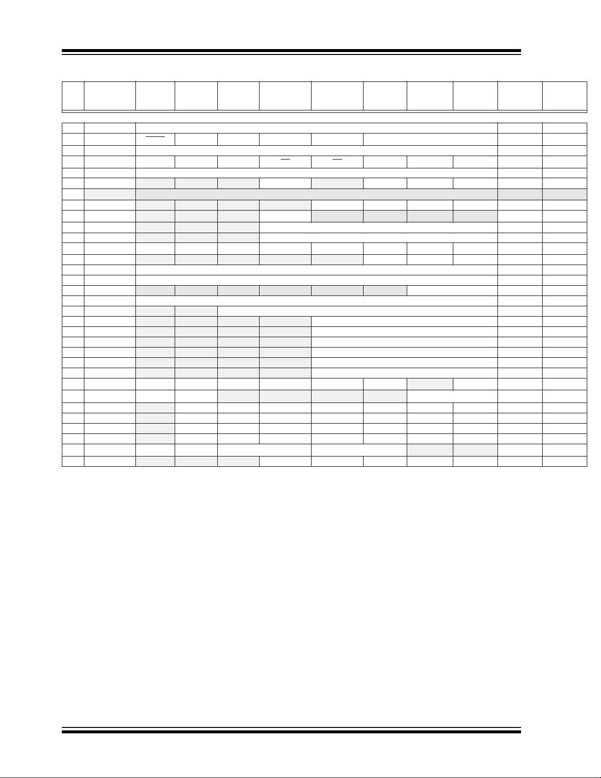
TABLE 2: 14/16-PIN ALLOCATION TABLE FOR PIC16F753/HV753
I/O
14-Pin PDIP/SOIC/TSSOP
RA0 13 12 AN0 FVROUT
RA1 12 11 AN1 VREF+
RA2 11 10 AN2 COG1FLT — C1OUT T0CKI — INT
RA3 4 3 — — — — T1G
RA4 3 2 AN3 — — — T1G
RA5 2 1 — — — — T1CKI — IOC Y — CLKIN
RC0 10 9 AN4 — OPA1IN+ C2IN0+ — — IOC — — —
RC1 9 8 AN5 — OPA1IN- C1IN1-
RC2 8 7 AN6 — OPA1OUT C1IN2-
RC3 7 6 AN7 — — C1IN3-
RC4 6 5 — COG1OUT1 — C2OUT — — IOC — — —
RC5 5 4 — COG1OUT0 — — — CCP1 IOC — — —
VDD 1 16 — — — — — — — — — VDD
VSS 14 13 — — — — — — — — — VSS
Note 1: Default location for peripheral pin function. Alternate location can be selected using the APFCON register.
2: Alternate location for peripheral pin function selected by the APFCON register.
16-Pin QFN
ADC
Reference
DACOUT
FVRIN
Op Amp
— C1IN0+ — — IOC Y — ICSPDAT
— C1IN0-
Comparator
C2IN0-
C2IN1-
C2IN2-
C2IN3-
Timer
— — IOC Y — ICSPCLK
(2)
(1)
— — IOC — — —
— — IOC — SLPCIN —
— — IOC — — —
CCP
IOC
— IOC Y — MCLR/
— IOC Y — CLKOUT
Pull-up
Interrupt
Y — —
Slope Compensation
Basic
PP
V
2013 Microchip Technology Inc. Preliminary DS40001709B-page 3

PIC16F753/HV753
Table of Contents
1.0 Device Overview ......................................................................................................................................................................... 6
2.0 Memory Organization .................................................................................................................................................................. 9
3.0 Flash Program Memory Self Read/Self Write Control ............................................................................................................... 25
4.0 Oscillator Module ....................................................................................................................................................................... 34
5.0 I/O Ports .................................................................................................................................................................................... 39
6.0 Timer0 Module .......................................................................................................................................................................... 54
7.0 Timer1 Module with Gate Control .............................................................................................................................................. 57
8.0 Timer2 Module .......................................................................................................................................................................... 68
9.0 Hardware Limit Timer (HLT) Module ......................................................................................................................................... 70
10.0 Capture/Compare/PWM Modules ............................................................................................................................................. 74
11.0 Complementary Output Generator (COG) Module .................................................................................................................... 81
12.0 Analog-to-Digital Converter (ADC) Module ............................................................................................................................. 104
13.0 Fixed Voltage Reference (FVR) .............................................................................................................................................. 115
14.0 Digital-to-Analog Converter (DAC) Module ............................................................................................................................. 117
15.0 Comparator Module ................................................................................................................................................................. 123
16.0 Operational Amplifier (OPA) Module ....................................................................................................................................... 132
17.0 Slope Compensator.................................................................................................................................................................. 135
18.0 Instruction Set Summary ......................................................................................................................................................... 140
19.0 Special Features of the CPU ................................................................................................................................................... 149
20.0 Shunt Regulator (PIC16HV753 Only) ...................................................................................................................................... 168
21.0 Development Support .............................................................................................................................................................. 169
22.0 Electrical Specifications ........................................................................................................................................................... 173
23.0 DC and AC Characteristics Graphs and Charts ...................................................................................................................... 197
24.0 Packaging Information ............................................................................................................................................................. 216
The Microchip Web Site .................................................................................................................................................................... 228
Customer Change Notification Service ............................................................................................................................................. 228
Customer Support ............................................................................................................................................................................. 228
Product Identification System ............................................................................................................................................................ 229
DS40001709B-page 4 Preliminary 2013 Microchip Technology Inc.

PIC16F753/HV753
TO OUR VALUED CUSTOMERS
It is our intention to provide our valued customers with the best documentation possible to ensure successful use of your Microchip
products. To this end, we will continue to improve our publications to better suit your needs. Our publications will be refined and
enhanced as new volumes and updates are introduced.
If you have any questions or comments regarding this publication, please contact the Marketing Communications Department via
E-mail at docerrors@microchip.com. We welcome your feedback.
Most Current Data Sheet
To obtain the most up-to-date version of this data sheet, please register at our Worldwide Web site at:
http://www.microchip.com
You can determine the version of a data sheet by examining its literature number found on the bottom outside corner of any page.
The last character of the literature number is the version number, (e.g., DS30000000A is version A of document DS30000000).
Errata
An errata sheet, describing minor operational differences from the data sheet and recommended workarounds, may exist for current
devices. As device/documentation issues become known to us, we will publish an errata sheet. The errata will specify the revision
of silicon and revision of document to which it applies.
To determine if an errata sheet exists for a particular device, please check with one of the following:
• Microchip’s Worldwide Web site; http://www.microchip.com
• Your local Microchip sales office (see last page)
When contacting a sales office, please specify which device, revision of silicon and data sheet (include literature number) you are
using.
Customer Notification System
Register on our web site at www.microchip.com to receive the most current information on all of our products.
2013 Microchip Technology Inc. Preliminary DS40001709B-page 5

PIC16F753/HV753
Flash
Program
Memory
13
Data Bus
8
14
Program
Bus
Instruction Reg
Program Counter
RAM
File
Registers
Direct Addr
7
RAM Addr
9
Addr MUX
Indirect
Addr
FSR Reg
STATUS Reg
MUX
ALU
W Reg
Instruction
Decode &
Control
Timing
Generation
CLKIN
CLKOUT
PORTA
8
8
8
3
8-Level Stack
64 Bytes
2K X 14
(13-Bit)
Power-up
Timer
Power-on
Reset
Watchdog
Timer
MCLR
VSS
Brown-out
Reset
Timer0 Timer1
RA0
RA1
RA2
RA3
RA4
RA5
Analog Comparator
T0CKI
INT
T1CKI
Configuration
Internal
Oscillator
and Reference
T1G
VDD
Block
C1IN0+/C2IN0+
C1IN0-/C2IN0-
C1IN1-
C2IN1-
C1OUT/C2OUT
Shunt Regulator
(PIC16HV753 only)
Capture/
Compare/
PWM
(CCP)
Hardware
Limit
Timer1
(HLT)
Complementary
Output
Generator
(COG)
Timer2
Fixed Voltage
Reference
(FVR)
Dual Range
DAC
PORTC
RC0
RC1
RC2
RC3
RC4
RC5
Op. Amp.
Slope
Compensator
1.0 DEVICE OVERVIEW
Block Diagrams and pinout descriptions of the devices
are shown in Figure 1-1 and Ta bl e 1- 1.
The PIC16F753/HV753 devices are covered by this
data sheet. They are available in 14-pin PDIP, SOIC,
TSSOP and 16-pin QFN packages.
FIGURE 1-1: PIC16F753/HV753 BLOCK DIAGRAM
DS40001709B-page 6 Preliminary 2013 Microchip Technology Inc.

PIC16F753/HV753
TABLE 1-1: PIC16F753/HV753 PINOUT DESCRIPTION
Name Function
RA0/AN0/C1IN0+/DACOUT/
FVROUT/ICSPDAT
RA1/AN1/C1IN0-/C2IN0-/
REF+/FVRIN/ICSPCLK
V
RA2/AN2/INT/C1OUT/
T0CKI/COG1FLT
(1)
(3)
/T1G
RA3
RA4/AN3/T1G
RA5/T1CKI/COG1OUT0
C2IN1-/CLKIN
RC0/AN4/OPA1IN+/C2IN0+ RC0 TTL CMOS General purpose I/O with IOC and WPU.
RC1/AN5/OPA1IN-/C1IN1-/
C2IN1-
Legend: AN = Analog input or output CMOS = CMOS compatible input or output
Note 1: Input only.
/VPP/MCLR
(2)
/CLKOUT RA4 TTL CMOS General purpose I/O with IOC and WPU.
TTL = TTL compatible input ST = Schmitt Trigger input with CMOS levels
HP = High Power HV = High Voltage
* Alternate pin function.
2: Default pin function via the APFCON register.
3: Alternate pin function via the APFCON register.
4: RA3 pull-up is enabled when pin is configured as MCLR
(4)
(3)
RA0 TTL HP General purpose I/O with IOC and WPU.
AN0 AN — A/D Channel 0 input.
C1IN0+ AN — Comparator C1 positive input.
DACOUT — AN DAC unbuffered Voltage Reference output.
FVROUT — AN DAC/FVR buffered Voltage Reference output.
ICSPDAT ST HP Serial Programming Data I/O.
RA1 TTL CMOS General purpose I/O with IOC and WPU.
AN1 AN — A/D Channel 1 input.
C1IN0- AN — Comparator C1 negative input.
C2IN0- AN — Comparator C2 negative input.
REF+ AN — A/D Positive Voltage Reference input.
V
FVRIN AN — Voltage reference input.
ICSPCLK ST — Serial Programming Clock.
RA2 ST HP General purpose I/O with IOC and WPU.
AN2 AN — A/D Channel 2 input.
INT ST — External interrupt.
C1OUT — HP Comparator C1 output.
T0CKI ST — Timer0 clock input.
COG1FLT ST — COG auto-shutdown fault input.
RA3 TTL — General purpose input with WPU.
T1G ST — Timer1 Gate input.
PP HV — Programming voltage.
V
MCLR
AN3 AN — A/D Channel 3 input.
T1G ST — Timer1 Gate input.
CLKOUT — CMOS F
/
RA5 TTL CMOS General purpose I/O with IOC and WPU.
T1CKI ST — Timer1 clock input.
CLKIN ST — External Clock input (EC mode).
AN4 AN — A/D Channel 4 input.
OPA1IN+ AN — Op amp positive input.
C2IN0+ AN — Comparator C2 positive input.
RC1 TTL CMOS General purpose I/O with IOC and WPU.
AN5 AN — A/D Channel 5 input.
OPA1IN- AN — Op amp negative input.
C1IN1- AN — Comparator C1 negative input.
C2IN1- AN — Comparator C2 negative input.
Input
Type
ST
Output
Typ e
—
Description
Master Clear w/internal pull-up.
OSC/4 output.
in Configuration Word.
2013 Microchip Technology Inc. Preliminary DS40001709B-page 7

PIC16F753/HV753
TABLE 1-1: PIC16F753/HV753 PINOUT DESCRIPTION (CONTINUED)
Name Function
RC2/AN6/SLPCIN/
OPA1OUT/C1IN2-/C2IN2-
RC3/AN7/C1IN3-/C2IN3- RC3 TTL CMOS General purpose I/O with IOC and WPU.
RC4/COG1OUT1/C2OUT RC4 TTL CMOS General purpose I/O with IOC and WPU.
RC5/COG1OUT0/CCP1 RC5 TTL CMOS General purpose I/O with IOC and WPU.
DD VDD Power — Positive supply.
V
V
SS VSS Power — Ground reference.
Legend: AN = Analog input or output CMOS = CMOS compatible input or output
Note 1: Input only.
TTL = TTL compatible input ST = Schmitt Trigger input with CMOS levels
HP = High Power HV = High Voltage
* Alternate pin function.
2: Default pin function via the APFCON register.
3: Alternate pin function via the APFCON register.
4: RA3 pull-up is enabled when pin is configured as MCLR
RC2 TTL CMOS General purpose I/O with IOC and WPU.
AN6 AN — A/D Channel 6 input.
OPA1OUT AN HP Op amp output.
C1IN2- AN — Comparator C1 negative input.
C2IN2- AN — Comparator C2 negative input.
AN7 AN — A/D Channel 7 input.
C1IN3- AN — Comparator C1 negative input.
C2IN3- AN — Comparator C2 negative input.
COG1OUT1 — CMOS COG output Channel 1.
C2OUT — HP Comparator C2 output.
COG1OUT0 — CMOS COG output Channel 0.
CCP1 — HP Capture/Compare/PWM 1.
Input
Type
Output
Typ e
Description
in Configuration Word.
DS40001709B-page 8 Preliminary 2013 Microchip Technology Inc.

PIC16F753/HV753
PC<12:0>
13
0000h
0004h
0005h
07FFh
0400h
1FFFh
Stack Level 1
Stack Level 8
Reset Vector
Interrupt Vector
On-chip Program
Memory
CALL, RETURN
RETFIE, RETLW
Stack Level 2
Shadows 0-07FFh
2.0 MEMORY ORGANIZATION
2.1 Program Memory Organization
The PIC16F753/HV753 has a 13-bit program counter
capable of addressing an 8K x 14 program memory
space. Only the first 2K x 14 (0000h-07FFh) is
physically implemented. Accessing a location above
these boundaries will cause a wrap-around within the
first 2K x 14 space for PIC16F753/HV753. The Reset
vector is at 0000h and the interrupt vector is at 0004h
(see Figure 2-1).
FIGURE 2-1: PROGRAM MEMORY MAP
AND STACK FOR THE
PIC16F753/HV753
2.2 Data Memory Organization
The data memory (see Figure 2-2) is partitioned into four
banks, which contain the General Purpose Registers
(GPR) and the Special Function Registers (SFR). The
Special Function Registers are located in the first 32
locations of each bank. Register locations 40h-6Fh in
Bank 0 are General Purpose Registers, implemented as
static RAM. Register locations 70h-7Fh in Bank 0 are
Common RAM and shared as the last 16 addresses in
all Banks. All other RAM is unimplemented and returns
‘0’ when read. The RP<1:0> bits of the STATUS register
are the bank select bits.
RP0
RP1
00 Bank 0 is selected
01 Bank 1 is selected
10 Bank 2 is selected
11 Bank 3 is selected
2.2.1 GENERAL PURPOSE REGISTER FILE
The register file is organized as 64 x 8 in the
PIC16F753/HV753. Each register is accessed, either
directly or indirectly, through the File Select Register
(FSR) (see Section 2.5 “Indirect Addressing, INDF
and FSR Registers”).
2.2.2 SPECIAL FUNCTION REGISTERS
The Special Function Registers are registers used by
the CPU and peripheral functions for controlling the
desired operation of the device (see Tab le 2 -1 ). These
registers are static RAM.
The special registers can be classified into two sets:
core and peripheral. The Special Function Registers
associated with the “core” are described in this section.
Those related to the operation of the peripheral features
are described in the section of that peripheral feature.
2013 Microchip Technology Inc. Preliminary DS40001709B-page 9

PIC16F753/HV753
Legend: = Unimplemented data memory locations, read as ‘0’.
BANK 0 BANK 1 BANK 2 BANK 3
INDF 00h INDF 80h INDF 100h INDF 180h
TMR0 01h OPTION_REG 81h TMR0 101h OPTION_REG 181h
PCL 02h PCL 82h PCL 102h PCL 182h
STATUS 03h STATUS 83h STATUS 103h STATUS 183h
FSR 04h FSR 84h FSR 104h FSR 184h
PORTA 05h TRISA 85h LATA 105h ANSELA 185h
—06h —86h — 106h — 186h
PORTC 07h TRISC 87h LATC 107h ANSELC 187h
IOCAF 08h IOCAP 88h IOCAN 108h APFCON 188h
IOCCF 09h IOCCP 89h IOCCN 109h OSCTUNE 189h
PCLATH 0Ah PCLATH 8Ah PCLATH 10Ah PCLATH 18Ah
INTCON 0Bh INTCON 8Bh INTCON 10Bh INTCON 18Bh
PIR1 0Ch PIE1 8Ch WPUA 10Ch
PMCON1 18Ch
PIR2 0Dh PIE2 8Dh WPUC 10Dh
PMCON2 18Dh
—0Eh — 8Eh SLRCONC 10Eh PMADRL 18Eh
TMR1L 0Fh OSCCON 8Fh PCON 10Fh
PMADRH 18Fh
TMR1H 10h
FVR1CON0 90h TMR2 110h PMDATL 190h
T1CON 11h DAC1CON0 91h
PR2 111h PMDATH 191h
T1GCON 12h
DAC1REFL 92h T2CON 112h COG1PHR 192h
CCPR1L 13h
DAC1REFH 93h HLTMR1 113h COG1PHF 193h
CCPR1H 14h
—94h HLTPR1 114h COG1BKR 194h
CCP1CON 15h
—95h HLT1CON0 115h COG1BKF 195h
—16h OPA1CON0 96h HLT1CON1 116h COG1DBR 196h
—17h —97h HLTMR2 117h COG1DBF 197h
—18h — 98h HLTPR2 118h COG1CON0 198h
—19h — 99h HLT2CON0 119h COG1CON1 199h
—1Ah — 9Ah HLT2CON1 11Ah COG1RIS 19Ah
— 1Bh CM2CON0 9Bh — 11Bh COG1RSIM 19Bh
ADRESL 1Ch CM2CON1 9Ch
— 11Ch COG1FIS 19Ch
ADRESH 1Dh CM1CON0 9Dh
— 11Dh COG1FSIM 19Dh
ADCON0 1Eh CM1CON1 9Eh SLPCCON0 11Eh COG1ASD0 19Eh
ADCON1 1Fh CMOUT 9Fh SLPCCON1 11Fh COG1ASD1 19Fh
General
Purpose
Register
80 Bytes
20h
General Purpose
Register
32 Bytes
A0h
BFh
Unimplemented
Read as ‘0’
120h
Unimplemented
Read as ‘0’
1A0h
Unimplemented
Read as ‘0’
C0h
EFh
6Fh
16Fh
170h
17Fh
1EFh
1F0h
1FFh
Common RAM
16 Bytes
70h
7Fh
Common RAM
(Accesses
70h – 7Fh)
F0h
FFh
Common RAM
(Accesses
70h – 7Fh)
Common RAM
(Accesses
70h – 7Fh)
FIGURE 2-2: DATA MEMORY MAP OF THE PIC16F753/HV753
DS40001709B-page 10 Preliminary 2013 Microchip Technology Inc.

PIC16F753/HV753
TABLE 2-1: PIC16F753/HV753 SPECIAL REGISTERS SUMMARY BANK 0
Addr Name Bit 7 Bit 6 Bit 5 Bit 4 Bit 3 Bit 2 Bit 1 Bit 0
Bank 0
00h INDF INDF<7:0> xxxx xxxx xxxx xxxx
01h TMR0 TMR0<7:0> xxxx xxxx uuuu uuuu
02h PCL PCL<7:0> 0000 0000 0000 0000
03h STATUS
04h FSR FSR<7:0> xxxx xxxx uuuu uuuu
05h PORTA
06h
— Unimplemented — —
07h PORTC
08h IOCAF
09h IOCCF
0Ah PCLATH
0Bh INTCON GIE PEIE T0IE INTE IOCIE T0IF INTF IOCIF 0000 0000 0000 0000
0Ch PIR1
0Dh PIR2
— Unimplemented — —
0Eh
0Fh
TMR1L TMR1L<7:0> xxxx xxxx uuuu uuuu
10h
TMR1H TMR1H<7:0> xxxx xxxx uuuu uuuu
11h
T1CON
12h
T1GCON
13h
CCPR1L CCPR1L<7:0>
14h
CCPR1H CCPR1H<7:0>
15h
CCP1CON
— Unimplemented — —
16h
17h
— Unimplemented — —
18h
— Unimplemented — —
— Unimplemented — —
19h
1Ah
— Unimplemented — —
1Bh
— Unimplemented — —
ADRESL Least Significant two bits of the left shifted result or eight bits of the right shifted result xxxx xxxx uuuu uuuu
1Ch
1Dh ADRESH Most Significant eight bits of the left shifted A/D result or two bits of the right shifted result xxxx xxxx uuuu uuuu
1Eh ADCON0 ADFM
1Fh
ADCON1
Legend: — = Unimplemented locations read as ‘0’, u = unchanged, x = unknown, q = value depends on condition shaded = unimplemented.
IRP RP1 RP0 TO
— —
— —
— —
— —
— — — PCLATH<4:0> ---0 0000 ---0 0000
TMR1GIF ADIF — — HLTMR2IF HLTMR1IF TMR2IF TMR1IF 00--0000 00--0000
— — C2IF C1IF — COG1IF — CCP1IF --00 -0-0 --00 -0-0
TMR1CS<1:0> T1CKPS<1:0> T1OSCEN T1SYNC
TMR1GE T1GPOL T1GTM T1GSPM T1GGO/
— —
—
— ADCS<2:0> — — —
RA5 RA4 RA3 RA2 RA1 RA0
RC5 RC4 RC3 RC2 RC1 RC0
IOCAF5 IOCAF4 IOCAF3 IOCAF2 IOCAF1 IOCAF0
IOCCF5 IOCCF4 IOCCF3 IOCCF2 IOCCF1 IOCCF0
DC1B<1:0> CCP1M<3:0>
CHS<3:0> GO/DONE
PD ZDCC
—
TMR1ON 0000 00-0 0000 00-0
DONE
T1GVAL T1GSS<1:0>
ADON
ADPREF1 -000 ---0 -000 ---0
Value on
POR/BOR
0001 1xxx 000q quuu
--xx xxxx --uu uuuu
--xx xxxx --uu uuuu
--00 0000 --00 0000
--00 0000 --00 0000
0000 0x00 0000 0x00
xxxx xxxx
xxxx xxxx
--00 0000 --00 0000
0-00 0000 0-00 0000
Value on
all other
Resets
uuuu uuuu
uuuu uuuu
2013 Microchip Technology Inc. Preliminary DS40001709B-page 11

PIC16F753/HV753
TABLE 2-2: PIC16F753/HV753 SPECIAL REGISTERS SUMMARY BANK 1
Addr Name Bit 7 Bit 6 Bit 5 Bit 4 Bit 3 Bit 2 Bit 1 Bit 0
Bank 1
80h INDF INDF<7:0> xxxx xxxx uuuu uuuu
81h OPTION_REG
82h PCL PCL<7:0> 0000 0000 0000 0000
83h STATUS
84h FSR FSR xxxx xxxx uuuu uuuu
85h TRISA — — TRISA5 TRISA4 TRISA3 TRISA2 TRISA1 TRISA0 --11 1111 --11 1111
86h — Unimplemented — —
87h TRISC — — TRISC5 TRISC4 TRISC3 TRISC2 TRISC1 TRISC0 --11 1111 --11 1111
88h IOCAP — — IOCAP5 IOCAP4 IOCAP3 IOCAP2 IOCAP1 IOCAP0 --00 0000 --00 0000
89h IOCCP — — IOCCP5 IOCCP4 IOCCP3 IOCCP2 IOCCP1 IOCCP0 --00 0000 --00 0000
8Ah PCLATH — — —PCLATH<4:0>---0 0000 ---0 0000
8Bh INTCON GIE PEIE T0IE INTE IOCIE T0IF INTF IOCIF 0000 0000 0000 0000
8Ch PIE1 TMR1GIE ADIE — — HLTMR2IE HLTMR1IE TMR2IE TMR1IE 00-- 0000 00-- 0000
8Dh PIE2 — — C2IE C1IE — COG1IE — CCP1IE --00 -0-0 --00 -0-0
8Eh — Unimplemented — —
8Fh OSCCON
90h FVR1CON0 FVREN FVRRDY FVROE FVRBUFSS1 FVRBUFSS0 — — FVRBUFEN 0000 0--0 0000 0--0
91h DAC1CON0 DACEN DACFM DACOE — DACPSS1 DACPSS0 — — 000- 00-- 000- 00--
92h DAC1REFL Least Significant bit of the left shifted result or eight bits of the right shifted DAC setting 0000 0000 0000 0000
93h DAC1REFH
94h — Unimplemented — —
95h
— Unimplemented — —
96h OPA1CON OPA1EN — — OPA1UGM OPA1NCH<1:0> OPA1PCH<1:0> 0--0 0000 0--0 0000
97h
— Unimplemented — —
98h — Unimplemented — —
99h
— Unimplemented — —
9Ah — Unimplemented — —
9Bh CM2CON0 C2ON C2OUT C2OE C2POL C2ZLF C2SP C2HYS C2SYNC 0000 0100 0000 0100
9Ch CM2CON1 C2INTP C2INTN C2PCH<2:0> C2NCH<2:0> 0000 0000 0000 0000
9Dh CM1CON0 C1ON C1OUT C1OE C1POL C1ZLF C1SP C1HYS C1SYNC 0000 0100 0000 0100
9Eh CM1CON1 C1INTP C1INTN C1PCH<2:0> C1NCH<2:0> 0000 0000 0000 0000
9Fh CMOUT — — — — — — MCOUT2 MCOUT1 ---- --00 ---- --00
Legend: — = Unimplemented locations read as ‘0’, u = unchanged, x = unknown, q = value depends on condition shaded = unimplemented.
RAPU
IRP RP1 RP0 TO
INTEDG T0CS T0SE PSA PS<2:0>
PD ZDC C
— —
Most Significant eight bits of the left shifted DAC setting or first bit of the right shifted result 0000 0000 0000 0000
IRCF<1:0>
—
HTS LTS
—
Value on
POR/BOR
1111 1111 1111 1111
0001 1xxx 000q quuu
--01 -00- --uu -uu-
Values on
all other
Resets
DS40001709B-page 12 Preliminary 2013 Microchip Technology Inc.

PIC16F753/HV753
TABLE 2-3: PIC16F753/HV753 SPECIAL REGISTERS SUMMARY BANK 2
Addr Name Bit 7 Bit 6 Bit 5 Bit 4 Bit 3 Bit 2 Bit 1 Bit 0
Bank 2
100h INDF
101h TMR0
102h PCL
103h STATUS
104h FSR
105h LATA — —LATA5LATA4— LATA 2 LAT A1 L ATA0 --xx -xxx --uu -uuu
106h — Unimplemented — —
107h LATC — — LATC5 LATC4 LATC3 LATC2 LATC1 LATC0 --xx xxxx --uu uuuu
108h IOCAN — — IOCAN5 IOCAN4 IOCAN3 IOCAN2 IOCAN1 IOCAN0 --00 0000 --00 0000
109h IOCCN — — IOCCN5 IOCCN4 IOCCN3 IOCCN2 IOCCN1 IOCCN0 --00 0000 --00 0000
10Ah PCLATH
10Bh INTCON
10Ch WPUA — — WPUA5 WPUA4 WPUA3 WPUA2 WPUA1 WPUA0 --11 1111 --11 1111
10Dh WPUC — — WPUC5 WPUC4 WPUC3 WPUC2 WPUC1 WPUC0 --11 1111 --11 1111
10Eh SLRCONC — — SLRC5 SLRC4 — — — — --00 ---- --00 ----
10Fh PCON — — — — — —PORBOR ---- --qq ---- --uu
110h
TMR2 TMR2<7:0> 0000 0000 0000 0000
111h PR2 PR2<7:0> 1111 1111 1111 1111
112 h T 2CO N — T2OUTPS<3:0> TMR2ON T2CKPS<1:0> -000 0000 -000 0000
113h HLTMR1 Holding Register for the 8-bit Hardware Limit Timer1 Count 0000 0000 0000 0000
114h HLTPR1 HLTMR1 Module Period Register 1111 1111 1111 1111
115h HLT1CON0 — H1OUTPS<3:0> H1ON H1CKPS<1:0> -000 0000 -000 0000
116h HLT1CON1 H1FES H1RES — H1ERS<2:0> H1FEREN H1REREN 11-0 0000 11-0 0000
117 h
HLTMR2 Holding Register for the 8-bit Hardware Limit Timer2 Count 0000 0000 0000 0000
118 h
HLTPR2 HLTMR2 Module Period Register 1111 1111 1111 1111
119 h
HLT2CON0
11A h
HLT2CON1 H2FES H2RES
11B h
— Unimplemented — —
11C h
— Unimplemented — —
11D h
— Unimplemented — —
11E h
SLPCCON0 SC1EN
11F h
SLPCCON1
Legend: — = Unimplemented locations read as ‘0’, u = unchanged, x = unknown, q = value depends on condition shaded = unimplemented.
IRP RP1 RP0 TO
— — —PCLATH<4:0>---0 0000 ---0 0000
GIE PEIE T0IE INTE IOCIE T0IF INTF IOCIF 0000 0000 0000 0000
— H2OUTPS<3:0> H2ON H2CKPS<1:0> -000 0000 -000 0000
— H2ERS<2:0> H2FEREN H2REREN 11-0 0000 11-0 0000
— — SC1POL SC1TSS<1:0> —SC1INS0-00 00-0 0-00 00-0
— — — SC1RNG SC1ISET<3:0> ---0 0000 ---0 0000
INDF<7:0>
TMR0<7:0>
PCL<7:0>
PD ZDC C
FSR<7:0>
Val ue o n
POR/BOR
xxxx xxxx xxxx xxxx
xxxx xxxx uuuu uuuu
0000 0000 0000 0000
0001 1xxx 000q quuu
xxxx xxxx uuuu uuuu
Valu e o n
all other
Resets
2013 Microchip Technology Inc. Preliminary DS40001709B-page 13
PIC16F753/HV753
TABLE 2-4: PIC16F753/HV753 SPECIAL FUNCTION REGISTERS SUMMARY BANK 3
Addr Name Bit 7 Bit 6 Bit 5 Bit 4 Bit 3 Bit 2 Bit 1 Bit 0
Bank 3
180h INDF INDF<7:0> xxxx xxxx uuuu uuuu
181h OPTION_REG
182h PCL PCL<7:0> 0000 0000 0000 0000
183h STATUS
184h FSR FSR<7 :0> xxxx xxxx uuuu uuuu
185h ANSELA — — —ANSA4 — ANSA2 ANSA1 ANSA0 ---1 -111 ---1 -111
186h
—
187h ANSELC — — — — ANSC3 ANSC2 ANSC1 ANSC0 ---- 0000 ---- 0000
188h APFCON
189h OSCTUNE — — — TUN<4:0> ---0 0000 ---0 0000
18Ah PCLATH — — — PCLATH<4:0> ---0 0000 ---0 0000
18Bh INTCON GIE PEIE T0IE INTE IOCIE T0IF INTF IOCIF
18Ch PMCON1 — — — — —WRENWR RD---- -000 ---- -000
18Dh PMCON2 Program Memory Control Register 2 ---- ---- ---- ----
18Eh PMADRL PMADRL<7:0> 0000 0000 0000 0000
18Fh PMADRH — — — — — — PMADRH<1:0> ---- --00 ---- --00
190h PMDATL PMDATL<7:0> 0000 0000 0000 0000
191h PMDATH — —PMDATH<5:0>--00 0000 --00 0000
192h COG1PHR — — — — G1PHR<3:0> ---- xxxx ---- uuuu
193h COG1PHF — — — —G1PHF<3:0>---- xxxx ---- uuuu
194h COG1BKR — — — — G1BKR<3:0> ---- xxxx ---- uuuu
195h COG1BKF — — — — G1BKF<3:0> ---- xxxx ---- uuuu
196h COG1DBR — — — —G1DBR<3:0>---- xxxx ---- uuuu
197h COG1DBF — — — —G1DBF<3:0>---- xxxx ---- uuuu
198h COG1CON0 G1EN G1OE1 G1OE0 G1POL1 G1POL0 G1LD
199h COG1CON1 G1RDBTS G1FDBTS
19Ah COG1RIS
19Bh COG1RSIM — G1RMHLT2 G1RMHLT1 G1RMT2M G1RMFLT G1RMCCP1 G1RMC2 G1RMC1 0000 0000 0000 0000
19Ch COG1FIS
19Dh COG1FSIM — G1FMHLT2 G1FMHLT1 G1FMT2M G1FMFLT G1FMCCP1 G1FMC2 G1FMC1 0000 0000 0000 0000
19Eh COG1ASD0 C1ASDE C1ARSEN G1ASD1L<1:0> G1ASD0L<1:0>
19Fh COG1ASD1
Legend: — = Unimplemented locations read as ‘0’, u = unchanged, x = unknown, q = value depends on condition shaded = unimplemented
RAPU
IRP RP1 RP0 TO
— — —
— G1RIHLT2 G1RIHLT1 G1RIT2M G1RIFLT G1RICCP1 G1RIC2 G1RIC1 0000 0000 0000 0000
— G1FIHLT2 G1FIHLT1 G1FIT2M G1FIFLT G1FICCP1 G1FIC2 G1FIC1 0000 0000 0000 0000
— — — G1ASDSHLT2 G1ASDSHLT1 G1ASDSC2 G1ASDSC1 G1ASDSFLT 0000 0000 0000 0000
INTEDG T0CS T0SE PSA PS<2:0>
PD ZDCC
Unimplemented
T1GSEL
— — — —
— — — — ---0 ---- ---0 ----
—
G1CS<1:0> 00-- --00 00-- --00
— —
G1MD 0000 00-0 0000 00-0
Val ue o n
POR/BOR
1111 1111 1111 1111
0001 1xxx 000q quuu
— —
0000 0000 0000 0000
0000 00-- 0000 00--
Values on
all other
Resets
DS40001709B-page 14 Preliminary 2013 Microchip Technology Inc.

PIC16F753/HV753
2.3 Global SFRs
writable. Therefore, the result of an instruction with the
STATUS register as destination may be different than
2.3.1 STATUS REGISTER
The STATUS register, shown in Register 2-1, contains:
• the arithmetic status of the ALU
• the Reset status
• the bank select bits for data memory (RAM)
The STATUS register can be the destination for any
instruction, like any other register. If the STATUS
register is the destination for an instruction that affects
the Z, DC or C bits, then the write to these three bits is
intended.
For example, CLRF STATUS, will clear the upper three
bits and set the Z bit. This leaves the STATUS register
as ‘000u u1uu’ (where u = unchanged).
It is recommended, therefore, that only BCF, BSF,
SWAPF and MOVWF instructions are used to alter the
STATUS register, because these instructions do not
affect any Status bits. For other instructions not
affecting any Status bits, see Section 18.0
“Instruction Set Summary”.
disabled. These bits are set or cleared according to the
device logic. Furthermore, the TO
and PD bits are not
REGISTER 2-1: STATUS: STATUS REGISTER
R/W-0 R/W-0 R/W-0 R-1 R-1 R/W-x R/W-x R/W-x
IRP RP1 RP0 TO
bit 7 bit 0
Legend:
R = Readable bit W = Writable bit U = Unimplemented bit, read as ‘0’
-n = Value at POR ‘1’ = Bit is set ‘0’ = Bit is cleared x = Bit is unknown
PD ZDC
(1)
(1)
C
bit 7 IRP: Register Bank Select bit (used for indirect addressing)
1 = Bank 2, 3 (100h-1FFh)
0 = Bank 0, 1 (00h-FFh)
bit 6 RP1: Register Bank Select bit (used for direct addressing)
00 = Bank 0 (00h-7Fh)
01 = Bank 1 (80h-FFh)
10 = Bank 2 (100h-17Fh)
11 = Bank 3 (180h-1FFh)
bit 5 RP0: Register Bank Select bit (used for direct addressing)
1 = Bank 1 (80h-FFh)
0 = Bank 0 (00h-7Fh)
bit 4 TO
bit 3 PD
bit 2 Z: Zero bit
bit 1 DC: Digit Carry/Borrow
bit 0 C: Carry/Borrow
: Time-Out bit
1 = After power-up, CLRWDT instruction or SLEEP instruction
0 = A WDT time-out occurred
: Power-Down bit
1 = After power-up or by the CLRWDT instruction
0 = By execution of the SLEEP instruction
1 = The result of an arithmetic or logic operation is zero
0 = The result of an arithmetic or logic operation is not zero
1 = A carry-out from the 4th low-order bit of the result occurred
0 = No carry-out from the 4th low-order bit of the result
bit
1 = A carry-out from the Most Significant bit of the result occurred
0 = No carry-out from the Most Significant bit of the result occurred
(2)
bit
(ADDWF, ADDLW,SUBLW,SUBWF instructions), For Borrow, the polarity is reversed.
(2)
(ADDWF, ADDLW, SUBLW, SUBWF instructions)
Note 1: The C and DC bits operate as a Borrow
instructions for examples.
2: For Borrow
For rotate (RRF, RLF) instructions, this bit is loaded with either the high-order or low-order bit of the source register.
2013 Microchip Technology Inc. Preliminary DS40001709B-page 15
, the polarity is reversed. A subtraction is executed by adding the two’s complement of the second operand.
and Digit Borrow out bit, respectively, in subtraction. See the SUBLW and SUBWF

PIC16F753/HV753
000
001
010
011
100
101
110
111
1 : 2
1 : 4
1 : 8
1 : 16
1 : 32
1 : 64
1 : 128
1 : 256
1 : 1
1 : 2
1 : 4
1 : 8
1 : 16
1 : 32
1 : 64
1 : 128
BIT VALUE TIMER0 RATE WDT RATE
2.3.2 OPTION REGISTER
The OPTION register is a readable and writable
register, which contains various control bits to
configure:
• Timer0/WDT prescaler
• External RA2/INT interrupt
•Timer0
• Weak pull-ups on PORTA
REGISTER 2-2: OPTION_REG: OPTION REGISTER
R/W-1 R/W-1 R/W-1 R/W-1 R/W-1 R/W-1 R/W-1 R/W-1
RAPU
bit 7 bit 0
Legend:
R = Readable bit W = Writable bit U = Unimplemented bit, read as ‘0’
-n = Value at POR ‘1’ = Bit is set ‘0’ = Bit is cleared x = Bit is unknown
INTEDG T0CS T0SE PSA PS<2:0>
Note: To achieve a 1:1 prescaler assignment for
Timer0, assign the prescaler to the WDT
by setting PSA bit to ‘1’ of the OPTION
register. See Section 6.1.3 “Software
Programmable Prescaler”.
bit 7 RAPU
: PORTA Pull-up Enable bit
1 = PORTA pull-ups are disabled
0 = PORTA pull-ups are enabled by individual PORT latch values
bit 6 INTEDG: Interrupt Edge Select bit
1 = Interrupt on rising edge of INT pin
0 = Interrupt on falling edge of INT pin
bit 5 T0CS: Timer0 Clock Source Select bit
1 = Transition on T0CKI pin
0 = Internal instruction cycle clock (F
bit 4 T0SE: Timer0 Source Edge Select bit
1 = Increment on high-to-low transition on T0CKI pin
0 = Increment on low-to-high transition on T0CKI pin
bit 3 PSA: Prescaler Assignment bit
1 = Prescaler is assigned to the WDT
0 = Prescaler is assigned to the Timer0 module
bit 2-0 PS<2:0>: Prescaler Rate Select bits
OSC/4)
DS40001709B-page 16 Preliminary 2013 Microchip Technology Inc.

PIC16F753/HV753
2.3.3 INTCON REGISTER
The INTCON register is a readable and writable
register, which contains the various enable and flag bits
for TMR0 register overflow, IOCIE change and external
RA2/INT pin interrupts.
Note: Interrupt flag bits are set when an interrupt
condition occurs, regardless of the state of
its corresponding enable bit or the Global
Enable bit, GIE of the INTCON register.
User software should ensure the
appropriate interrupt flag bits are clear
prior to enabling an interrupt.
REGISTER 2-3: INTCON: INTERRUPT CONTROL REGISTER
R/W-0 R/W-0 R/W-0 R/W-0 R/W-0 R/W-0 R/W-0 R/W-0
GIE PEIE T0IE INTE IOCIE T0IF INTF IOCIF
bit 7 bit 0
Legend:
R = Readable bit W = Writable bit U = Unimplemented bit, read as ‘0’
-n = Value at POR ‘1’ = Bit is set ‘0’ = Bit is cleared x = Bit is unknown
bit 7 GIE: Global Interrupt Enable bit
1 = Enables all unmasked interrupts
0 = Disables all interrupts
bit 6 PEIE: Peripheral Interrupt Enable bit
1 = Enables all unmasked peripheral interrupts
0 = Disables all peripheral interrupts
bit 5 T0IE: Timer0 Overflow Interrupt Enable bit
1 = Enables the Timer0 interrupt
0 = Disables the Timer0 interrupt
bit 4 INTE: RA2/INT External Interrupt Enable bit
1 = Enables the RA2/INT external interrupt
0 = Disables the RA2/INT external interrupt
bit 3 IOCIE: Interrupt-on-Change Interrupt Enable bit
1 = Enables the IOC change interrupt
0 = Disables the IOC change interrupt
bit 2 T0IF: Timer0 Overflow Interrupt Flag bit
1 = Timer0 register has overflowed (must be cleared in software)
0 = Timer0 register did not overflow
bit 1 INTF: RA2/INT External Interrupt Flag bit
1 = The RA2/INT external interrupt occurred (must be cleared in software)
0 = The RA2/INT external interrupt did not occur
bit 0 IOCIF: Interrupt-on-Change Interrupt Flag bit
1 = An IOC pin has changed state and generated an interrupt
0 = No pin interrupts have been generated
(2)
(1)
Note 1: IOC register must also be enabled.
2: T0IF bit is set when TMR0 rolls over. TMR0 is unchanged on Reset and should be initialized before
clearing T0IF bit.
2013 Microchip Technology Inc. Preliminary DS40001709B-page 17

PIC16F753/HV753
2.3.4 PIE1 REGISTER
The PIE1 register contains the Peripheral Interrupt
Enable bits, as shown in Register 2-4.
REGISTER 2-4: PIE1: PERIPHERAL INTERRUPT ENABLE REGISTER 1
R/W-0 R/W-0 U-0 U-0 R/W-0 R/W-0 R/W-0 R/W-0
TMR1GIE ADIE — — HLTMR2IE HLTMR1IE TMR2IE TMR1IE
bit 7 bit 0
Legend:
R = Readable bit W = Writable bit U = Unimplemented bit, read as ‘0’
-n = Value at POR ‘1’ = Bit is set ‘0’ = Bit is cleared x = Bit is unknown
bit 7 TMR1GIE: ADC Interrupt Enable bit
1 = Enables the TMR1 gate interrupt
0 = Disables the TMR1 gate interrupt
bit 6 ADIE: ADC Interrupt Enable bit
1 = Enables the ADC interrupt
0 = Disables the ADC interrupt
bit 5-4 Unimplemented: Read as ‘0’
bit 3 HLTMR2IE: HLT2 Interrupt Enable bit
1 = Enables the HLT2 interrupt
0 = Disables the HLT2 interrupt
bit 2 HLTMR1IE: HLT1 Interrupt Enable bit
1 = Enables the HLT1 interrupt
0 = Disables the HLT1 interrupt
bit 1 TMR2IE: Timer2 Interrupt Enable bit
1 = Enables the Timer2 interrupt
0 = Disables the Timer2 interrupt
bit 0 TMR1IE: Timer1 Interrupt Enable bit
1 = Enables the Timer1 interrupt
0 = Disables the Timer1 interrupt
Note: Bit PEIE of the INTCON register must be
set to enable any peripheral interrupt.
DS40001709B-page 18 Preliminary 2013 Microchip Technology Inc.

PIC16F753/HV753
2.3.5 PIE2 REGISTER
The PIE2 register contains the Peripheral Interrupt
Enable bits, as shown in Register 2-5.
REGISTER 2-5: PIE2: PERIPHERAL INTERRUPT ENABLE REGISTER 1
U-0 U-0 R/W-0 R/W-0 U-0 R/W-0 U-0 R/W-0
— —C2IEC1IE—COG1IE — CCP1IE
bit 7 bit 0
Legend:
R = Readable bit W = Writable bit U = Unimplemented bit, read as ‘0’
-n = Value at POR ‘1’ = Bit is set ‘0’ = Bit is cleared x = Bit is unknown
bit 7-6 Unimplemented: Read as ‘0’
bit 5 C2IE: Comparator 2 Interrupt Enable bit
1 = Enables the Comparator 2 interrupt
0 = Disables the Comparator 2 interrupt
bit 4 C1IE: Comparator 1 Interrupt Enable bit
1 = Enables the Comparator 1 interrupt
0 = Disables the Comparator 1 interrupt
bit 3 Unimplemented: Read as ‘0’
bit 2 COG1IE: COG 1 Interrupt Flag bit
1 = COG1 interrupt enabled
0 = COG1 interrupt disabled
bit 1 Unimplemented: Read as ‘0’
bit 0 CCP1IE: CCP1 Interrupt Enable bit
1 = Enables the CCP1 interrupt
0 = Disables the CCP1 interrupt
Note: Bit PEIE of the INTCON register must be
set to enable any peripheral interrupt.
2013 Microchip Technology Inc. Preliminary DS40001709B-page 19

PIC16F753/HV753
2.3.6 PIR1 REGISTER
The PIR1 register contains the Peripheral Interrupt flag
bits, as shown in Register 2-6.
REGISTER 2-6: PIR1: PERIPHERAL INTERRUPT REQUEST REGISTER 1
R/W-0 R/W-0 U-0 U-0 R/W-0 R/W-0 R/W-0 R/W-0
TMR1GIF ADIF
bit 7 bit 0
Legend:
R = Readable bit W = Writable bit U = Unimplemented bit, read as ‘0’
-n = Value at POR ‘1’ = Bit is set ‘0’ = Bit is cleared x = Bit is unknown
bit 7 TMR1GIF: TMR1 Gate Interrupt Flag bit
1 = Timer1 gate interrupt is pending
0 = Timer1 gate interrupt is not pending
bit 6 ADIF: ADC Interrupt Flag bit
1 = ADC conversion complete
0 = ADC conversion has not completed or has not been started
bit 5-4 Unimplemented: Read as ‘0’
bit 3 HLTMR2IF: HLT2 to HLTPR2 Match Interrupt Flag bit
1 = HLT2 to HLTPR2 match occurred (must be cleared in software)
0 = HLT2 to HLTPR2 match did not occur
bit 2 HLTMR1IF: HLT1 to HLTPR1 Match Interrupt Flag bit
1 = HLT1 to HLTPR1 match occurred (must be cleared in software)
0 = HLT1 to HLTPR1 match did not occur
bit 1 TMR2IF: Timer2 to PR2 Match Interrupt Flag bit
1 = Timer2 to PR2 match occurred (must be cleared in software)
0 = Timer2 to PR2 match did not occur
bit 0 TMR1IF: Timer1 Interrupt Flag bit
1 = Timer1 rolled over (must be cleared in software)
0 = Timer1 has not rolled over
— — HLTMR2IF HLTMR1IF TMR2IF TMR1IF
Note: Interrupt flag bits are set when an interrupt
condition occurs, regardless of the state of
its corresponding enable bit or the Global
Enable bit, GIE of the INTCON register.
User software should ensure the
appropriate interrupt flag bits are clear prior
to enabling an interrupt.
DS40001709B-page 20 Preliminary 2013 Microchip Technology Inc.

PIC16F753/HV753
2.3.7 PIR2 REGISTER
The PIR2 register contains the Peripheral Interrupt flag
bits, as shown in Register 2-7.
REGISTER 2-7: PIR2: PERIPHERAL INTERRUPT REQUEST REGISTER 1
U-0 U-0 R/W-0 R/W-0 U-0 R/W-0 U-0 R/W-0
— — C2IF C1IF —COG1IF— CCP1IF
bit 7 bit 0
Legend:
R = Readable bit W = Writable bit U = Unimplemented bit, read as ‘0’
-n = Value at POR ‘1’ = Bit is set ‘0’ = Bit is cleared x = Bit is unknown
bit 7-6 Unimplemented: Read as ‘0’
bit 5 C2IF: Comparator 1 Interrupt Flag bit
1 = Comparator output (C2OUT bit) has changed (must be cleared in software)
0 = Comparator output (C2OUT bit) has not changed
bit 4 C1IF: Comparator 1 Interrupt Flag bit
1 = Comparator output (C1OUT bit) has changed (must be cleared in software)
0 = Comparator output (C1OUT bit) has not changed
bit 3 Unimplemented: Read as ‘0’
bit 2 COG1IF: COG 1 Interrupt Flag bit
1 = COG1 has generated an auto-shutdown interrupt
0 = COG1 has NOT generated an auto-shutdown interrupt
bit 1 Unimplemented: Read as ‘0’
bit 0 CCP1IF: ECCP Interrupt Flag bit
Capture Mode
1 = A TMR1 register capture occurred (must be cleared in software)
0 = No TMR1 register capture occurred
Compare Mode
1 = A TMR1 register compare match occurred (must be cleared in software)
0 = No TMR1 register compare match occurred
PWM mode
Unused in this mode
Note: Interrupt flag bits are set when an interrupt
condition occurs, regardless of the state of
its corresponding enable bit or the Global
Enable bit, GIE of the INTCON register.
User software should ensure the
appropriate interrupt flag bits are clear prior
to enabling an interrupt.
2013 Microchip Technology Inc. Preliminary DS40001709B-page 21

PIC16F753/HV753
2.3.8 PCON REGISTER
The Power Control (PCON) register (see Tab le 19 -2 )
contains flag bits to differentiate between a:
• Power-on Reset (POR
• Brown-out Reset (BOR)
• Watchdog Timer Reset (WDT)
• External MCLR
The PCON register also controls the software enable of
the BOR
The PCON register bits are shown in Register 2-8.
.
REGISTER 2-8: PCON: POWER CONTROL REGISTER
U-0 U-0 U-0 U-0 U-0 U-0 R/W-q/u R/W-q/u
— — — — — —PORBOR
bit 7 bit 0
Legend:
R = Readable bit W = Writable bit U = Unimplemented bit, read as ‘0’
u = Bit is unchanged x = Bit is unknown -n/n = Value at POR and BOR/Value at all other Resets
‘1’ = Bit is set ‘0’ = Bit is cleared q = unchanged
)
Reset
bit 7-2 Unimplemented: Read as ‘0’
bit 1 POR
bit 0 BOR
: Power-on Reset Status bit
1 = No Power-on Reset occurred
0 = A Power-on Reset occurred (must be set in software after a Power-on Reset occurs)
: Brown-out Reset Status bit
1 = No Brown-out Reset occurred
0 = A Brown-out Reset occurred (must be set in software after a Brown-out Reset occurs)
DS40001709B-page 22 Preliminary 2013 Microchip Technology Inc.

PIC16F753/HV753
PC
12 8 7 0
5
PCLATH<4:0>
PCLATH
Instruction with
ALU Result
GOTO, CALL
OPCODE <10:0>
8
PC
12 11 10 0
11
PCLATH<4:3>
PCH PCL
87
2
PCLATH
PCH PCL
PCL as
Destination
MOVLW 0x40 ;initialize pointer
MOVWF FSR ;to RAM
NEXT CLRF INDF ;clear INDF register
INCF FSR ;inc pointer
BTFSS FSR,7 ;all done?
GOTO NEXT ;no clear next
CONTINUE ;yes continue
2.4 PCL and PCLATH
The Program Counter (PC) is 13 bits wide. The low byte
comes from the PCL register, which is a readable and
writable register. The high byte (PC<12:8>) is not directly
readable or writable and comes from PCLATH. On any
Reset, the PC is cleared. Figure 2-3 shows the two
situations for the loading of the PC. The upper example
in Figure 2-3 shows how the PC is loaded on a write to
PCL (PCLATH<4:0> PCH). The lower example in
Figure 2-3 shows how the PC is loaded during a CALL or
GOTO instruction (PCLATH<4:3> PCH).
FIGURE 2-3: LOADING OF PC IN
DIFFERENT SITUATIONS
2.4.2 STACK
The PIC16F753/HV753 Family has an 8-level x 13-bit
wide hardware stack (see Figure 2-1). The stack space
is not part of either program or data space and the
Stack Pointer is not readable or writable. The PC is
PUSHed onto the stack when a CALL instruction is executed or an interrupt causes a branch. The stack is
POPed in the event of a RETURN, RETLW or a RETFIE
instruction execution. PCLATH is not affected by a
PUSH or POP operation.
The stack operates as a circular buffer. This means that
after the stack has been PUSHed eight times, the ninth
push overwrites the value that was stored from the first
push. The tenth push overwrites the second push (and
so on).
Note 1: There are no Status bits to indicate Stack
Overflow or Stack Underflow conditions.
2: There are no instructions/mnemonics
called PUSH or POP. These are actions
that occur from the execution of the
CALL, RETURN, RETLW and RETFIE
instructions or the vectoring to an
interrupt address.
2.5 Indirect Addressing, INDF and FSR Registers
2.4.1 MODIFYING PCL
Executing any instruction with the PCL register as the
destination simultaneously causes the Program
Counter PC<12:8> bits (PCH) to be replaced by the
contents of the PCLATH register. This allows the entire
contents of the program counter to be changed by
writing the desired upper five bits to the PCLATH
register. When the lower eight bits are written to the
PCL register, all 13 bits of the program counter will
change to the values contained in the PCLATH register
and those being written to the PCL register.
A computed GOTO is accomplished by adding an offset
to the program counter (ADDWF PCL). Care should be
exercised when jumping into a look-up table or
program branch table (computed GOTO) by modifying
the PCL register. Assuming that PCLATH is set to the
table start address, if the table length is greater than
255 instructions or if the lower eight bits of the memory
address rolls over from 0xFF to 0x00 in the middle of
the table, then PCLATH must be incremented for each
address rollover that occurs between the table
beginning and the target location within the table.
For more information refer to Application Note AN556,
“Implementing a Table Read” (DS00556).
The INDF register is not a physical register. Addressing
the INDF register will cause indirect addressing.
Indirect addressing is possible by using the INDF
register. Any instruction using the INDF register
actually accesses data pointed to by the File Select
Register (FSR). Reading INDF itself indirectly will
produce 00h. Writing to the INDF register indirectly
results in a no operation (although Status bits may be
affected). An effective 9-bit address is obtained by
concatenating the 8-bit FSR and the IRP bit of the
STATUS register, as shown in Figure 2-4.
A simple program to clear RAM location 40h-7Fh using
indirect addressing is shown in Example 2-1.
EXAMPLE 2-1: INDIRECT ADDRESSING
2013 Microchip Technology Inc. Preliminary DS40001709B-page 23

PIC16F753/HV753
Data
Memory
Indirect AddressingDirect Addressing
Bank Select Location Select
RP1 RP0 6
0
From Opcode
IRP File Select Register
7
0
Bank Select
Location Select
00 01 10 11
180h
1FFh
00h
7Fh
Bank 0 Bank 1 Bank 2 Bank 3
For memory map detail, see Figure 2-2.
FIGURE 2-4: DIRECT/INDIRECT ADDRESSING PIC16F753/HV753
DS40001709B-page 24 Preliminary 2013 Microchip Technology Inc.

PIC16F753/HV753
3.0 FLASH PROGRAM MEMORY SELF READ/SELF WRITE CONTROL
The Flash program memory is readable and writable
during normal operation (full V
is not directly mapped in the register file space.
Instead, it is indirectly addressed through the Special
Function Registers (see Registers 3-1 to 3-5). There
are six SFRs used to read and write this memory:
•PMCON1
•PMCON2
•PMDATL
•PMDATH
• PMADRL
• PMADRH
When interfacing the program memory block, the
PMDATL and PMDATH registers form a two-byte word
which holds the 14-bit data for read/write, and the
PMADRL and PMADRH registers form a two-byte
word which holds the 10-bit address of the Flash location being accessed. These devices have 1K words of
program Flash with an address range from 0000h to
03FFh.
The program memory allows a single-word read and a
four-word write. A four-word write automatically erases
the row of the location and writes the new data (erase
before write).
The write time is controlled by an on-chip timer. The
write/erase voltages are generated by an on-chip
charge pump rated to operate over the voltage range
of the device for byte or word operations.
When the device is code-protected, the CPU may
continue to read and write the Flash program memory.
Depending on the settings of the Flash Program
Memory Enable (WRT<1:0>) bits, the device may or
may not be able to write certain blocks of the program
memory; however, reads of the program memory are
allowed.
When the Flash program memory Code Protection
) bit in the Configuration Word register is enabled,
(CP
the program memory is code-protected, and the
device programmer (ICSP™) cannot access data or
program memory.
DD range). This memory
3.1 PMADRH and PMADRL Registers
The PMADRH and PMADRL registers can address up
to a maximum of 1K words of program memory.
When selecting a program address value, the Most
Significant Byte (MSB) of the address is written to the
PMADRH register and the Least Significant Byte
(LSB) is written to the PMADRL register.
3.2 PMCON1 and PMCON2 Registers
PMCON1 is the control register for the data program
memory accesses.
Control bits RD and WR initiate read and write,
respectively. These bits cannot be cleared, only set in
software. They are cleared in hardware at completion
of the read or write operation. The inability to clear the
WR bit in software prevents the accidental premature
termination of a write operation.
The WREN bit, when set, will allow a write operation.
On power-up, the WREN bit is clear.
PMCON2 is not a physical register. Reading PMCON2
will read all ‘0’s. The PMCON2 register is used
exclusively in the Flash memory write sequence.
2013 Microchip Technology Inc. Preliminary DS40001709B-page 25

PIC16F753/HV753
3.3 Register Definitions: Flash Program Memory Control
REGISTER 3-1: PMDATL: PROGRAM MEMORY DATA LOW BYTE REGISTER
R/W-0 R/W-0 R/W-0 R/W-0 R/W-0 R/W-0 R/W-0 R/W-0
PMDATL<7:0>
bit 7 bit 0
Legend:
R = Readable bit W = Writable bit U = Unimplemented bit, read as ‘0’
-n = Value at POR ‘1’ = Bit is set ‘0’ = Bit is cleared x = Bit is unknown
bit 7-0 PMDATL<7:0>: Eight Least Significant Data bits to Write or Read from Program Memory
REGISTER 3-2: PMADRL: PROGRAM MEMORY ADDRESS LOW BYTE REGISTER
R/W-0 R/W-0 R/W-0 R/W-0 R/W-0 R/W-0 R/W-0 R/W-0
PMADRL<7:0>
bit 7 bit 0
Legend:
R = Readable bit W = Writable bit U = Unimplemented bit, read as ‘0’
-n = Value at POR ‘1’ = Bit is set ‘0’ = Bit is cleared x = Bit is unknown
bit 7-0 PMADRL<7:0>: Eight Least Significant Address bits for Program Memory Read/Write Operation
REGISTER 3-3: PMDATH: PROGRAM MEMORY DATA HIGH BYTE REGISTER
U-0 U-0 R/W-0 R/W-0 R/W-0 R/W-0 R/W-0 R/W-0
— —PMDATH<5:0>
bit 7 bit 0
Legend:
R = Readable bit W = Writable bit U = Unimplemented bit, read as ‘0’
-n = Value at POR ‘1’ = Bit is set ‘0’ = Bit is cleared x = Bit is unknown
bit 7-6 Unimplemented: Read as ‘0’
bit 5-0 PMDATH<5:0>: Six Most Significant Data bits from Program Memory
REGISTER 3-4: PMADRH: PROGRAM MEMORY ADDRESS HIGH BYTE REGISTER
U-0 U-0 U-0 U-0 U-0 U-0 R/W-0 R/W-0
— — — — — — PMADRH<1:0>
bit 7 bit 0
Legend:
R = Readable bit W = Writable bit U = Unimplemented bit, read as ‘0’
-n = Value at POR ‘1’ = Bit is set ‘0’ = Bit is cleared x = Bit is unknown
bit 7-2 Unimplemented: Read as ‘0’
bit 1-0 PMADRH<1:0>: Specifies the two Most Significant Address bits or High bits for Program Memory
Reads.
DS40001709B-page 26 Preliminary 2013 Microchip Technology Inc.

PIC16F753/HV753
REGISTER 3-5: PMCON1: PROGRAM MEMORY CONTROL 1 REGISTER
U-0 U-0 U-0 U-0 U-0 R/W-0/0 R/S/HC-0/0 R/S/HC-0/0
— — — — —WRENWR RD
bit 7 bit 0
Legend:
R = Readable bit W = Writable bit U = Unimplemented bit, read as ‘0’
S = Bit can only be set x = Bit is unknown -n/n = Value at POR and BOR/Value at all other Resets
‘1’ = Bit is set ‘0’ = Bit is cleared HC = Bit is cleared by hardware
bit 7-3 Unimplemented: Read as ‘0’
bit 2 WREN: Program/Erase Enable bit
1 = Allows program/erase cycles
0 = Inhibits programming/erasing of program Flash
bit 1 WR: Write Control bit
1 = Initiates a program Flash program/erase operation
The operation is self-timed and the bit is cleared by hardware once operation is complete.
The WR bit can only be set (not cleared) in software.
0 = Program/erase operation to the Flash is complete and inactive
bit 0 RD: Read Control bit
1 = Initiates a program Flash read. Read takes one cycle. RD is cleared in hardware. The RD bit can
only be set (not cleared) in software.
0 = Does not initiate a program Flash read
REGISTER 3-6: PMCON2: PROGRAM MEMORY CONTROL 2 REGISTER
W-0/0 W-0/0 W-0/0 W-0/0 W-0/0 W-0/0 W-0/0 W-0/0
Program Memory Control Register 2
bit 7 bit 0
Legend:
R = Readable bit W = Writable bit U = Unimplemented bit, read as ‘0’
S = Bit can only be set x = Bit is unknown -n/n = Value at POR and BOR/Value at all other Resets
‘1’ = Bit is set ‘0’ = Bit is cleared
bit 7-0 Flash Memory Unlock Pattern bits:
To unlock writes, a 55h must be written first, followed by an AAh, before setting the WR bit of the
PMCON1 register. The value written to this register is used to unlock the writes. There are specific
timing requirements on these writes.
2013 Microchip Technology Inc. Preliminary DS40001709B-page 27

PIC16F753/HV753
BANKSEL PM_ADR ; Change STATUS bits RP1:0 to select bank with PMADRL
MOVLW MS_PROG_PM_ADDR ;
MOVWF PMADRH ; MS Byte of Program Address to read
MOVLW LS_PROG_PM_ADDR ;
MOVWF PMADRL ; LS Byte of Program Address to read
BANKSEL PMCON1 ; Bank to containing PMCON1
BSF PMCON1, RD ; PM Read
NOP ; First instruction after BSF PMCON1,RD executes normally
NOP ; Any instructions here are ignored as program
; memory is read in second cycle after BSF PMCON1,RD
;
BANKSEL PMDATL ; Bank to containing PMADRL
MOVF PMDATL, W ; W = LS Byte of Program PMDATL
MOVF PMDATH, W ; W = MS Byte of Program PMDATL
3.4 Reading the Flash Program Memory
To read a program memory location, the user must
write two bytes of the address to the PMADRL and
PMADRH registers, and then set control bit RD
(PMCON1<0>). Once the read control bit is set, the
program memory Flash controller will use the second
instruction cycle after to read the data. This causes the
second instruction immediately following the “
PMCON1,RD
” instruction to be ignored. The data is
available in the very next cycle in the PMDATL and
PMDATH registers; it can be read as two bytes in the
following instructions. PMDATL and PMDATH registers will hold this value until another read or until it is
written to by the user (during a write operation).
EXAMPLE 3-1: FLASH PROGRAM READ
BSF
DS40001709B-page 28 Preliminary 2013 Microchip Technology Inc.

PIC16F753/HV753
Q1 Q2 Q3 Q4 Q1 Q2 Q3 Q4 Q1 Q2 Q3 Q4 Q1 Q2 Q3 Q4 Q1 Q2 Q3 Q4 Q1 Q2 Q3 Q4
BSF PMCON1,RD
Executed here
INSTR (PC + 1)
Executed here
NOP
Executed here
PC PC + 1 PMADRH,PMADRL PC+3 PC + 5
Flash ADDR
RD bit
INSTR (PC)
PMDATH,PMDATL
INSTR (PC + 3)
PC + 3 PC + 4
INSTR (PC + 4)
INSTR (PC + 1)
INSTR (PC - 1)
Executed here
INSTR (PC + 3)
Executed here
INSTR (PC + 4)
Executed here
Flash DATA
PMDATH
PMDATL
Register
PMRHLT
FIGURE 3-1: FLASH PROGRAM MEMORY READ CYCLE EXECUTION
2013 Microchip Technology Inc. Preliminary DS40001709B-page 29

PIC16F753/HV753
3.5 Writing the Flash Program
Memory
A word of the Flash program memory may only be
written to if the word is in an unprotected segment of
memory.
Flash program memory must be written in four-word
blocks. See Figure 3-2 and Figure 3-3 for more details.
A block consists of four words with sequential
addresses, with a lower boundary defined by an
address, where PMADRL<1:0> = 00. All block writes to
program memory are done as 16-word erase by fourword write operations. The write operation is edgealigned and cannot occur across boundaries.
To write program data, it must first be loaded into the
buffer registers (see Figure 3-2). This is accomplished
by first writing the destination address to PMADRL and
PMADRH and then writing the data to PMDATL and
PMDATH. After the address and data have been set
up, then the following sequence of events must be
executed:
1. Write 55h, then AAh, to PMCON2 (Flash
programming sequence).
2. Set the WR control bit of the PMCON1 register.
All four buffer register locations should be written to
with correct data. If less than four words are being
written to in the block of four words, then a read from
the program memory location(s) not being written to
must be performed. This takes the data from the
program location(s) not being written and loads it into
the PMDATL and PMDATH registers. Then the
sequence of events to transfer data to the buffer
registers must be executed.
To transfer data from the buffer registers to the program
memory, the PMADRL and PMADRH must point to the
last location in the four-word block (PMADRL<1:0> =
11). Then the following sequence of events must be
executed:
1. Write 55h, then AAh, to PMCON2 (Flash
programming sequence).
2. Set control bit WR of the PMCON1 register to
begin the write operation.
The user must follow the same specific sequence to
initiate the write for each word in the program block,
writing each program word in sequence (000, 001,
010, 011). When the write is performed on the last
word (PMADRL<1:0> = 11), a block of sixteen words is
automatically erased and the content of the four-word
buffer registers are written into the program memory.
After the “BSF PMCON1,WR” instruction, the processor
requires two cycles to set up the erase/write operation.
The user must place two NOP instructions after the WR
bit is set. Since data is being written to buffer registers,
the writing of the first three words of the block appears
to occur immediately. The processor will halt internal
operations for the typical 4 ms, only during the cycle in
which the erase takes place (i.e., the last word of the
sixteen-word block erase). This is not Sleep mode as
the clocks and peripherals will continue to run. After
the four-word write cycle, the processor will resume
operation with the third instruction after the PMCON1
write instruction. The above sequence must be
repeated for the higher 12 words.
3.6 Protection Against Spurious Write
There are conditions when the device should not write
to the program memory. To protect against spurious
writes, various mechanisms have been built in. On
power-up, WREN is cleared. Also, the Power-up Timer
(64 ms duration) prevents program memory writes.
The write initiate sequence and the WREN bit help
prevent an accidental write during brown-out, power
glitch or software malfunction.
3.7 Operation During Code-Protect
When the device is code-protected, the CPU is able to
read and write unscrambled data to the program
memory.
3.8 Operation During Write Protect
When the program memory is write-protected, the CPU
can read and execute from the program memory. The
portions of program memory that are write-protected
can be modified by the CPU using the PMCON
registers, but the protected program memory cannot be
modified using ICSP mode.
DS40001709B-page 30 Preliminary 2013 Microchip Technology Inc.
 Loading...