

PIC12C67X
8-Pin, 8-Bit CMOS Microcontroller with A/D Converter
and EEPROM Data Memory
Devices Included in this Data Sheet:
• PIC12C671
• PIC12C672
•PIC12CE673
•PIC12CE674
Note: Throughout this data sheet PIC12C67X
refers to the PIC12C671, PIC12C672,
PIC12CE673 and PIC12CE674.
PIC12CE67X refers to PIC12CE673 and
PIC12CE674.
High-Performance RISC CPU:
• Only 35 single word instructions to learn
• All instructions are sin gle cycle (400 ns) e xcept f or
program branches which are two-cycle
• Operating speed: DC - 10 MHz clock input
DC - 400 ns instruction cycle
Memory
Device
Program
Data
RAM
Data
EEPROM
PIC12C671 1024 x 14 128 x 8 —
PIC12C672 2048 x 14 128 x 8 —
PIC12CE673 1024 x 14 128 x 8 16 x 8
PIC12CE674 2048 x 14 128 x 8 16 x 8
• 14-bit wide instructions
• 8-bit wide data path
• Interrupt capability
• Special function hardware registers
• 8-level deep hardware stack
• Direct, indirect and relative addressing modes for
data and instructions
Peripheral Features:
• Four-channel, 8-bit A/D converter
• 8-bit real time clock/counter (TMR0) with 8-bit
programmable prescaler
• 1,000,000 erase/write cycle EEPROM data
memory
• EEPROM data retention > 40 years
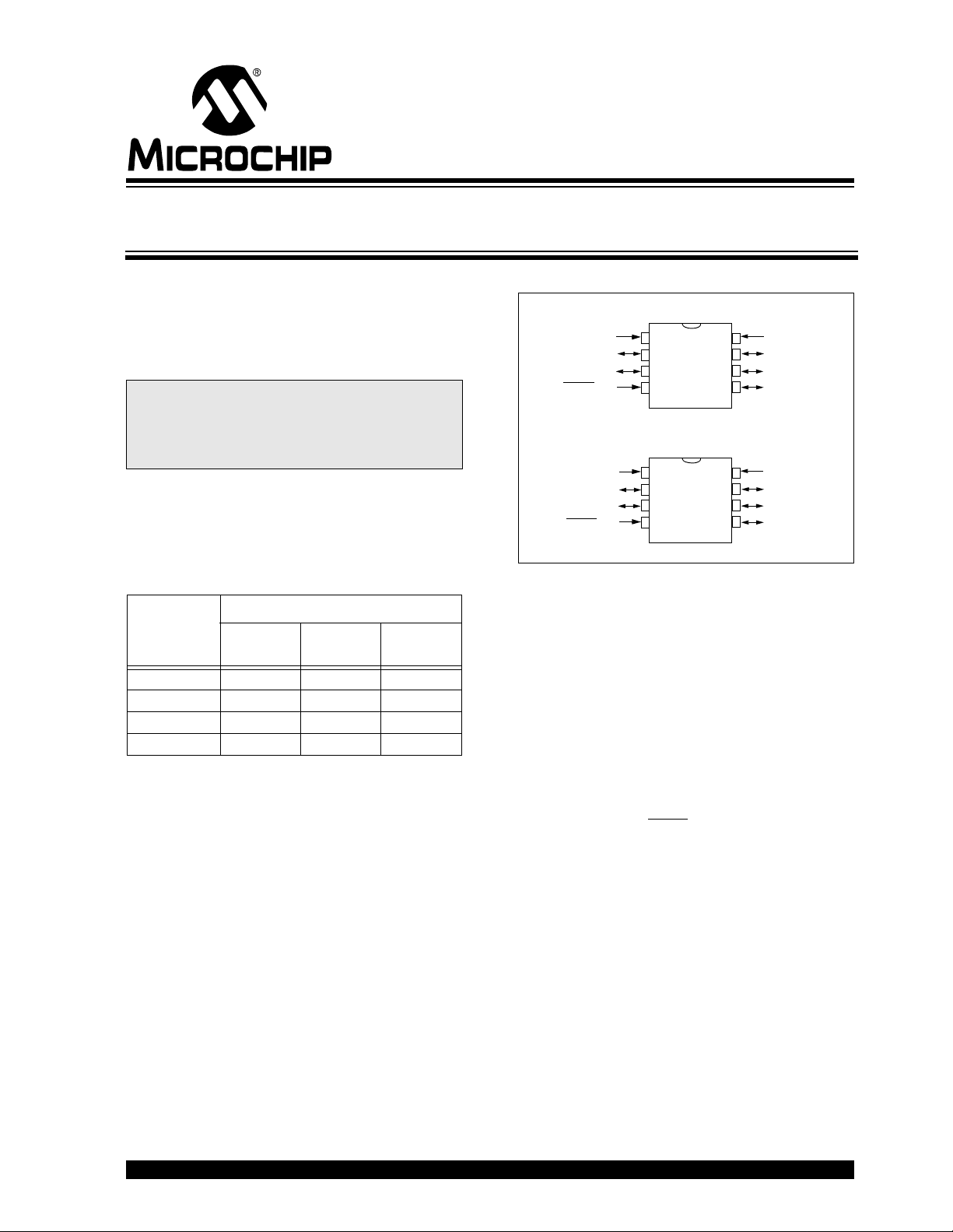
Pin Diagrams :
PDIP, SOIC, Windowed CERDIP
PIC12C671
VDD
GP5/OSC1/CLKIN
GP4/OSC2/AN3/
CLKOUT
GP3/MCLR
PDIP, Windowed CERDIP
GP5/OSC1/CLKIN
GP4/OSC2/AN3/
GP3/MCLR
/VPP
VDD
CLKOUT
/VPP
1
2
3
4
1
2
3
4
PIC12C672
PIC12CE673
PIC12CE674
8
7
6
5
8
7
6
5
VSS
GP0/AN0
GP1/AN1/V
GP2/T0CKI/AN2/
INT
VSS
GP0/AN0
GP1/AN1/V
GP2/T0CKI/AN2/
INT
REF
REF
Special Microcontroller Features:
• In-Circu it Serial Programming (ICSP™)
• Internal 4 MHz oscillator with progra mmab le ca libr ation
• Selectable clockout
• Power-on Reset (POR)
• Power-up Timer (PWRT) and Oscillator Start-up
Timer (OST)
• Watchdog Timer (WDT) with its own on-chip RC
oscillator for reliable operation
• Programmable code protection
• Po w er saving SLEEP mode
• Interrupt-on-pin change (GP0, GP1, GP3)
• Internal pull-ups on I/O pins (GP0, GP1, GP3)
• Internal pull-up on MCLR
pin
• Selectable oscillator options:
- INTRC: Precision internal 4 MHz oscillator
- EXTRC: External low-cost RC oscillator
- XT: Standard crystal/resonator
- HS: High speed crystal/resonator
- LP: Power saving, low frequency crystal
CMOS Technology:
• Low-power , high-speed CMOS EPROM/EEPROM
technolog y
• Fully static design
• Wide operating voltage range 2.5V to 5.5V
• Commercial, Industrial and Extended
temperature ranges
• Low power consumption
< 2 mA @ 5V, 4 MHz
15 µA typical @ 3V, 32 kHz
< 1 µA typical standby current
1999 Microchip Technology Inc. DS30561B-page 1

PIC12C67X
Table of Contents
1.0 General Description ......................................................... .... .. .. ....... .... .. .. .... .. ....... .. .... .. .... .............................................................3
2.0 PIC12C67X Device Vari e ties.................... ........................................................................................ ............................................ 5
3.0 Architectural Overview..................................................................................................................................................................7
4.0 Memory Organization. . ................................................................................................................................................................11
5.0 I/O Port........................................................................................................................................................................................25
6.0 EEPROM Peripheral Operation .................................................................... ....... .... .. .... .. ....... ....................................................33
7.0 Timer0 Module............................................................................................................................................................................39
8.0 Analog-to-Digital Converter (A/D) Module................................................................................................................................... 45
9.0 Special Features of the CPU.......................................................................................................................................................53
10.0 Instruction Set Summary............................................................................................................................................................. 69
11.0 Development Support ................................................................................................................................................................. 83
12.0 Electrical Specifications..............................................................................................................................................................89
13.0 DC and AC Characteristics .................................................. .... ....... .... .. .... .... ....... .. .... .. .... .........................................................109
14.0 Packaging Information....................................................................................................... ....................................................... 115
Appendix A:Compatibility................................. ........................... ........................... ........................ ....................................................119
Appendix B:Code for Accessing EEPROM Data Memory ................................................................................................................. 119
Index ....................................... .. .. .. .. .. .. ................................................... .. .. .. .. .. ..................................................................................121
On-Line Support........................................................... ....... .... .. .... .... ....... .... .... .. .... ....... .....................................................................125
Reader Response.............................................................................................................................................................................. 126
PIC12C67X Product Identification System ................................................................................. .......................................................127
To Our Val ued Customers
Most Current Data Sheet
To automatically obtain the most up-to-date version of this data sheet, please register at our Worldwide Web site at:
http://www.microchip.com
You can determine the version of a data sheet by examining its literature number found on the bottom outside corner of any page.
The last character of the literature number is the version number. e.g., DS30000A is version A of document DS30000.
New Customer Notification System
Register on our web site (www.microchip.com/cn) to receive the most current information on our products.
Errata
An errata sheet may exist for current devices, describing minor operational differences (from the data sheet) and recommended
workarounds. As device/documentation issues become known to us, w e will pub lish an errata sheet. The errata will specify the re vision of silicon and revision of document to which it applies.
To determine if an errata sheet exists for a particular device, please check with one of the following:
• Microchip’s Worldwide Web site; http://www.microchip.com
• Your local Microchip sales office (see last page)
• The Microchip Corporate Literature Center; U.S. FAX: (480) 786-7277
When contacting a sales office or the literature center, please specify which device, revision of silicon and data sheet (include liter-
ature number) you are using.
Corrections to this Data Sheet
We constantly strive to improve the quality of all our products and documentation. We have spent a great deal of time to ensure
that this document is correct. However , w e realize that we ma y ha v e missed a f ew things . If y ou find any inf ormation that is missi n g
or appears in error, please:
• Fill out and mail in the reader response form in the back of this data sheet.
• E-mail us at webmaster@microchip.com.
We appreciate your assistance in making this a better document.
DS30561B-page 2
1999 Microchip Technology Inc.

PIC12C67X
1.0 GENERAL DESCRIPTION
The PIC12C67X devices are low-cost, high-performance, CMOS, fully-static, 8-bit microcontrollers with
integrated analog-to-digital (A/D) converter and
EEPROM data memory (EEPROM on PIC12CE67X
versions only).
®
All PICmicro
RISC architecture. The PIC12C67X microcontrollers
have enhanced core features, eight-level deep stack,
and multiple internal and external interrupt sources.
The separate instruction and data buses of the Harvard
architecture allow a 14-bit wide instruction word with
the separate 8-bit wide data. The two stage instruction
pipeline allows all instructions to execute in a single
cycle, except for program branches, which require two
cycles. A total of 35 instructions (reduced instruction
set) are avai lable. Ad ditionally, a large register set give s
some of the architectu ral inno v ations us ed to achie v e a
very high performance.
PIC12C67X microcontrollers typically achieve a 2:1
code compression and a 4:1 speed improvement over
other 8-bit microcontrollers in their class.
The PIC12C67X devices have 128 bytes of RAM, 16
bytes of EEPR OM data memo ry (PIC12CE67X only), 5
pins and 1 input pin. In addition a timer/counter is
I/O
available. Also a 4-channel, high-speed, 8-bit A/D is
provided. The 8 -bi t res ol utio n i s i dea lly s uited for applications requiring low-cost analog interface, (i.e.,
thermostat control, pressure sensing, etc.)
The PIC12C67X devices have special features to
reduce external components, thus reducing cost,
enhancing system reliability and reducing power consumption. The Power-On Reset (POR), Power-up
Timer (PWRT), and Oscillator Start-up Timer (OST)
eliminate the need f or e xternal rese t circuitry . There are
five oscillator configurations to choose from, including
INTRC precision internal oscillator mode and the
power-saving LP (Low Power) oscillator mode. Powersaving SLEEP mode, Watchdog Timer and code
protection features improve system cost, power and
reliability. The SLEEP (power-down) f eat ure pro vides a
power-saving mode. The user can wake-up the chip
from SLEEP through several external and internal
interrupts and resets.
microcontrollers employ an advanced
A highly reliable Watchdog Timer with its own on-chip
RC oscillator provides protection against software
lock-up.
A UV erasable windowe d package version is ide al for
code development, while the cost-effective One-TimeProgrammable (OTP) version is suitable for production
in any vo lume. Th e custom er can ta ke f ull adv antag e of
Microchip’s pr ice leadership in OTP microcontrollers,
while benefiting from the OTP’s flexibility.
1.1 Applications
The PIC12C67X series fits perfectly in applications
ranging from personal care appliances and security
systems to low-power remote transmitters/receivers.
The EPROM technology makes customizing application programs (transmitter codes, appliance settings,
receiver frequencies, etc.) extremely fast and convenient, while the EEPROM data memory (PIC12CE67X
only) technology allows for the changing of calibration
factors and security codes. The small footprint packages, for through hole or surface mounting, make this
microcontroller series perfect for applications with
space limitations. Low-cost, low-power, high performance, ease of use and I/O flexibility make the
PIC12C67X series very versatile even in areas where
no microcontroller use has been considered before
(i.e., timer functions, replacement of "glue" logic and
PLD’s in larger systems, coprocessor applications).
1.2 Family and Upward Compatibility
The PIC12C67X products are compatible with other
members of the 14-bit PIC16CXXX families.
1.3 Development Support
The PIC12C67X devices are supported by a fullfeatured macro assembler, a software simulator, an incircuit emulator, a low-cost development programmer
and a full-featured programmer. A “C” compiler and
fuzzy logic support tools are also available.
1999 Microchip Technology Inc. DS30561B-page 3

PIC12C67X
TABLE 1-1: PIC12C67X & PIC12CE67X FAMILY OF DEVICES
PIC12C671 PIC12LC671 PIC12C672 PIC12LC672 PIC12CE673 PIC12LCE673 PIC12CE674 PIC12LCE674
Clock
Memory
Peripherals
Features
Maximum
Frequency
of Operation
(MHz)
EPROM
Program
Memory
RAM Data
Memory
(bytes)
EEPROM
Data Memory
(bytes)
Timer
Module(s)
A/D Converter (8-bit)
Channels
Wake-up
from SLEEP
on pin
change
Interrupt
Sources
I/O Pins 5 5 5 5 5 5 5 5
Input Pins 1 1 1 1 1 1 1 1
Internal
Pull-ups
In-Circuit
Serial
Programming
Number of
Instructions
Voltage
Range (Volts)
Packages 8-pin DIP,
10 10 10 10 10 10 10 10
1024 x 14 1024 x 14 2048 x 14 2048 x 14 1024 x 14 1024 x 14 2048 x 14 2048 x 14
128 128 128 128
—— ——
TMR0 TMR0 TMR0 TMR0 TMR0 TMR0 TMR0 TMR0
44 44 44 44
Yes Yes Yes Yes Yes Yes Yes Yes
44 44 44 44
Yes Yes Yes Yes Yes Yes Yes Yes
Yes Yes Yes Yes Yes Yes Yes Yes
35 35 35 35 35 35 35 35
3.0V - 5.5V 2.5V - 5.5V 3.0V - 5.5V 2.5V - 5.5V 3.0V - 5.5V 2.5V - 5.5V 3.0V - 5.5V 2.5V - 5.5V
JW, SOIC
8-pin DIP,
JW, SOIC
8-pin DIP,
JW, SOIC
8-pin DIP ,
JW, SOIC
128 128 128 128
16 16 16 16
8-pin DIP, JW8-pin DIP,JW8-pin DIP, JW8-pin DIP,
JW
All PIC12C67X devices have Power-on Reset, selectable W atchdog Timer, selectable code protect and high I/O current capability.
All PIC12C67X devices use serial programming with data pin GP0 and clock pin GP1.
DS30561B-page 4
1999 Microchip Technology Inc.

PIC12C67X
2.0 PIC12C67X DEVICE VARIETIES
A variety of frequency ranges and packaging options
are avai lable . Dependin g on applicati on and production
requirements, th e proper de vice option ca n be selected
using the information in the PIC12C67X Product Identification System section at the end of this data sheet.
When placing orders, please use that page of the data
sheet to specify the correct part number.
For e xample, the PIC12C67X device “type” is indicate d
in the device number:
1. C, as in PIC12C671. These devices have
EPROM type memory and operate over the
standard voltage range.
2. LC, as in PIC12LC671. These devices have
EPROM type memory and operate over an
extended voltage range.
3. CE, as in PIC12CE674. These devices have
EPROM type memory, EEPROM data memory
and operate over the standard voltage range.
4. LCE, as in PIC 12LCE674. These devices have
EPROM type memory, EEPROM data memory
and operate over an extended voltage ran ge.
2.1 UV Erasable Devices
The UV erasable version, offered in windowed package, is optimal f or prototy pe de v elopment a nd pilot p rograms.
The UV erasable version can be erased and reprogrammed to any of the configuration modes.
Microchip's PICSTART
grammers both support the PIC12C67X. Third party
programmers also are available; refer to the Microchip
Third Party Guide for a list of sources.
Note: Please note that erasing the device will
also erase the pre-programmed internal
calibration value for the internal oscillator.
The calibration value must be saved prior
to erasing the part.
Plus and PRO MATE pro-
2.3 Quick-Turn-Programming (QTP) Devices
Microchip offers a QTP Programming Service for factory production orders. This service is made available
for users who choose not to program a medium to high
quantity of units and whose code patterns have stabilized. The de vic es are i dentical to the OTP devices, but
with all EPROM locations and configuration options
already programmed by the factory. Certain code and
prototype verification procedures apply before production shipments are available. Please contact your local
Microchip Technology sales office for more details.
2.4 Serialized Quick-Turn Programming (SQTPSM) Devices
Microchip offers a unique programming service where
a few user-defined locations in each device are programmed with different serial numbers. The serial numbers may be random, pseudo-random, or sequential.
Serial programming allows each device to have a
unique number which can serve as an entry-code,
password, or ID number.
2.2 One-Time-Programm able (OTP) Devices
The availability of OTP devices is especially useful for
customers who need the flexibility for frequent code
updates and small volume applications.
The OTP devices, packaged in plastic packages, permit the user to program them once. In addition to the
program memory, the configuration bits must also be
programmed.
1999 Microchip Technology Inc. DS30561B-page 5

PIC12C67X
NOTES:
DS30561B-page 6
1999 Microchip Technology Inc.

PIC12C67X
3.0 ARCHITECTURAL OVERVIEW
The high perf ormance o f the PIC 12C67 X f a mily ca n b e
attributed to a number of architectural features commonly found in RISC microprocessor s. To begi n with,
the PIC12C67X uses a Harvard architecture, in which
program and data are accessed from separate memories using separate buses. This improves bandwidth
over tr aditional von Neu mann archi tecture in wh ich program and data are fetched from the same memory
using the same bus. Separating program and data
buses also allow instruction s to be size d differen tly than
the 8-bit wi de data word. Inst ruction opc odes are 14bits wide making it possible to have all single word
instructions. A 14-bit wide program memory access
bus fetches a 14-bit i nstruction in a single instru ction
cycle. A two-stage pipeline overlaps fetch and execution of instructions (Example 3-1). Consequently, all
instructions (35) e xec ute in a single cycle (40 0 ns @ 10
MHz) except for program branches.
The table below lists program memory (EPROM), data
memory (RAM), and non-volatile memory (EEPROM)
for each PIC12C67X device.
Device
PIC12C671 1K x 14 128 x 8 —
PIC12C672 2K x 14 128 x 8 —
PIC12CE673 1K x 14 128 x 8 16x8
PIC12CE674 2K x 14 128 x 8 16x8
Program
Memory
RAM Data
Memory
EEPROM
Data
Memory
The PIC12C67X can directly or indirectly address its
register files or data mem ory. All special function registers, including the program counter, are mapped in the
data memory. The PIC12C67X has an orthogonal
(symmetrical) instruction set that makes it possible to
carry out any operation on any register using any
addressing mode. This symmetrical nature and lack of
‘special optimal situations’ make progra mmi ng w ith th e
PIC12C67X simple yet efficient. In addition, the learning curve is reduced significantly.
PIC12C67X devices contain an 8-bit ALU and working
register. The ALU is a general purpose arithmetic unit.
It performs arithmetic and Boolean functions between
the data in the working register and any register file.
The ALU is 8-bits wide and capable of addition, subtraction, shift and logical operations. Unless otherwise
mentioned, arithmetic operations are two's complement in nature. In two-operand instructions, typically
one operand is the working register (W register). The
other operand is a file register or an immediate constant. In single operand instructions, the operand is
either the W register or a file register.
The W register is an 8-bit working register use d for ALU
operations. It is not an addressable register.
Depending on the instruction executed, the ALU may
affect the v alu es of th e Ca rry (C), Digit Carry (DC), an d
Zero (Z) bits in th e STA T US regis ter . The C and DC bits
operate as a borrow
respectively, in subtra cti on. See th e S UBLW a nd SUBWF
instructions for examples.
bit and a digit borrow out bit,
1999 Microchip Technology Inc. DS30561B-page 7
PIC12C67X
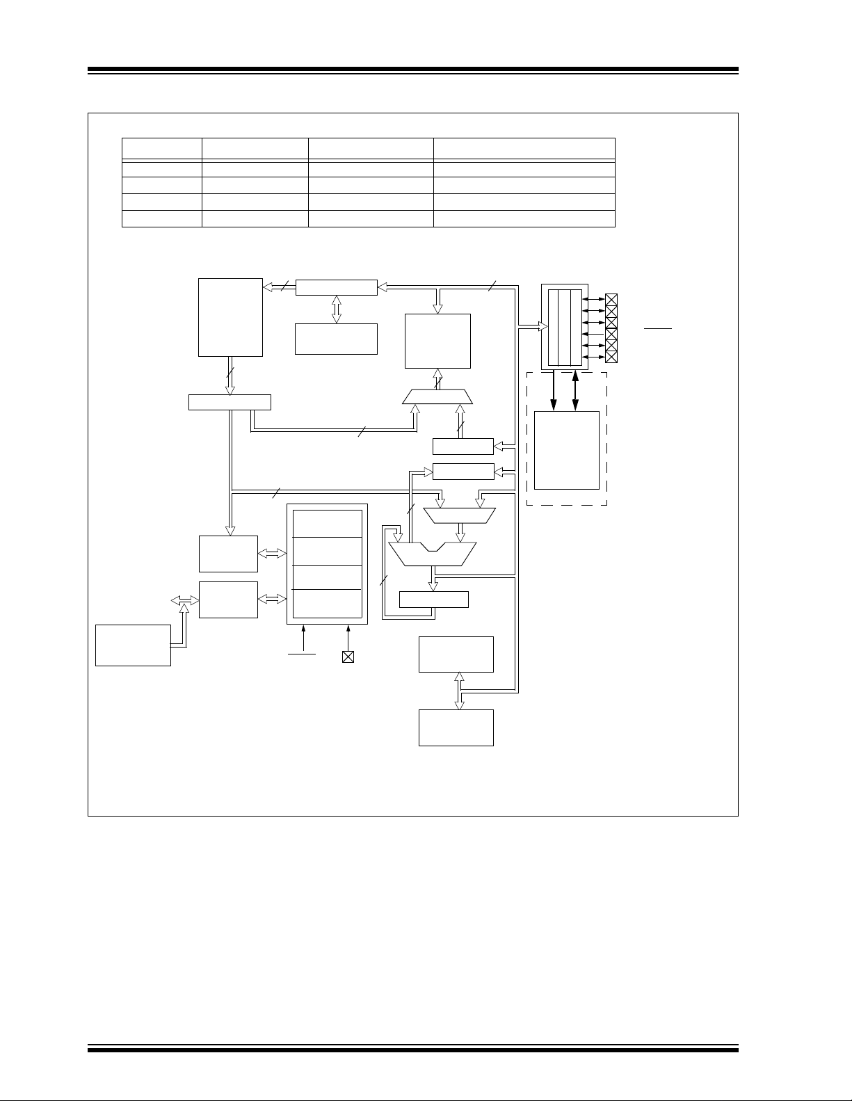
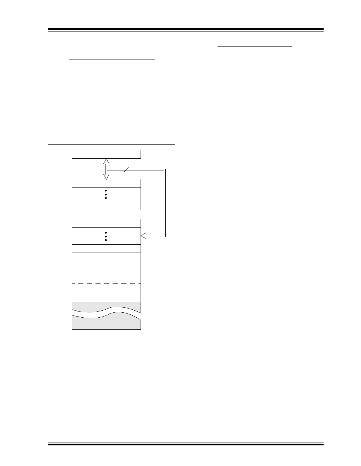
FIGURE 3-1: PIC12C67X BLOCK DIAGRAM
Device Program Memory Data Memory (RAM) Non-Volatile Memory (EEPROM)
PIC12C671 1K x 14 128 x 8 —
PIC12C672 2K x 14 128 x 8 —
PIC12CE673 1K x 14 128 x 8 16 x 8
PIC12CE674 2K x 14 128 x 8 16 x 8
OSC1/CLKIN
OSC2/CLKOUT
Internal
4 MHz Clock
Program
Bus
EPROM
Program
Memory
14
Instruction reg
Instruction
Decode &
Control
Timing
Generation
13
Program Counter
8 Level Stack
Direct Addr
8
Power-up
Oscillator
Start-up Tim er
Watchdog
Power-on
MCLR
(13 bit)
Timer
Timer
Reset
VDD, VSS
RAM Addr
7
3
8
Data Bus
RAM
128 bytes
File
Registers
(1)
Addr MUX
8
FSR reg
STATUS reg
ALU
W reg
Timer0
9
MUX
Indirect
Addr
8
GPIO
SCL
16x8
EEPROM
Data
Memory
GP0/AN0
GP1/AN1/VREF
GP2/T0CKI/AN2/INT
GP3/MCLR/VPP
GP4/OSC2/AN3/CLKOUT
GP5/OSC1/CLKIN
SDA
PIC12CE673
PIC12CE674
Note 1: Higher order bits are from the STATUS Register.
DS30561B-page 8
A/D
1999 Microchip Technology Inc.
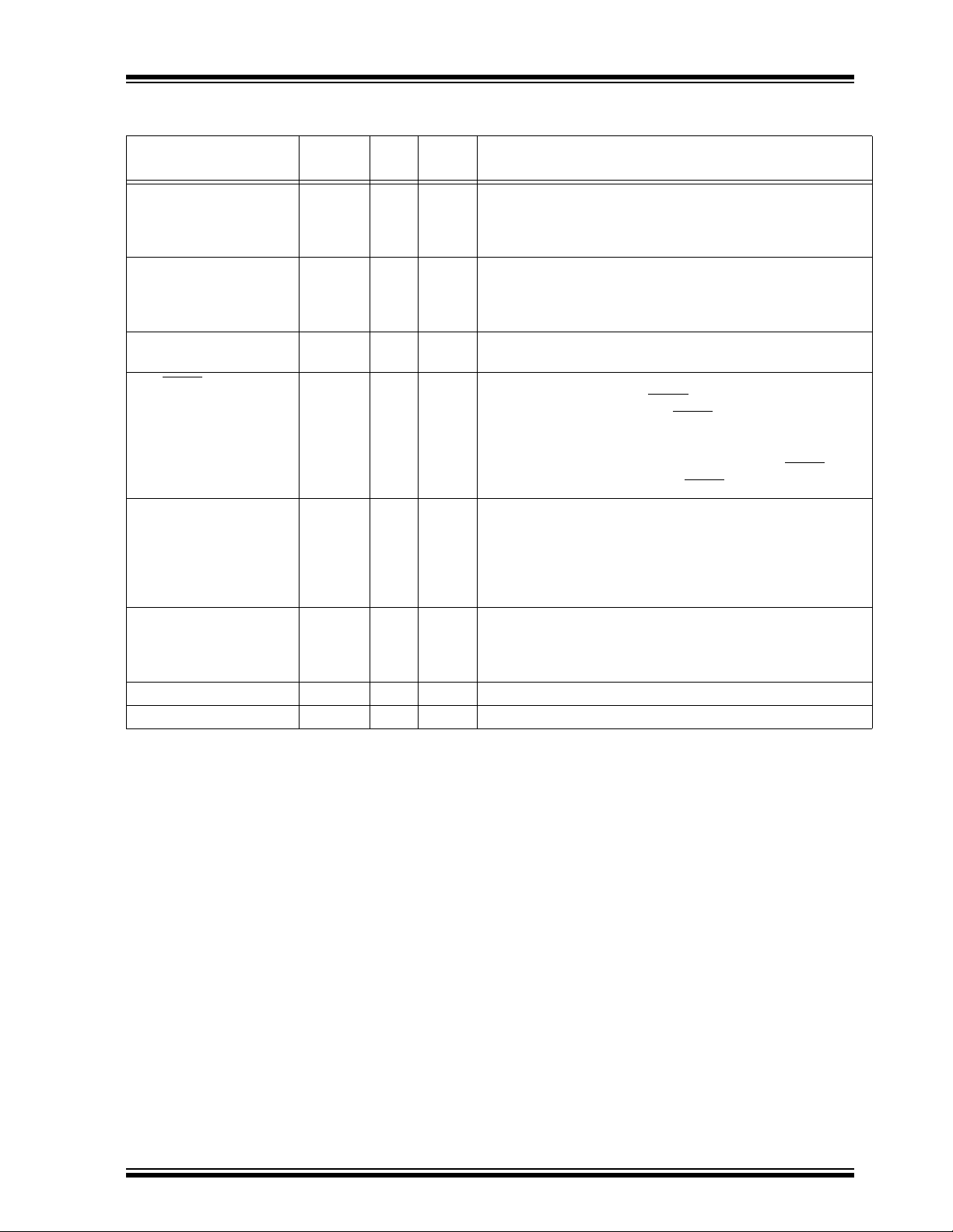
TABLE 3-1: PIC12C67X PINOUT DESCRIPTION
PIC12C67X
Name DIP Pin #
GP0/AN0 7 I/O TTL/ST Bi-directional I/O port/serial programming data/analog input 0.
GP1/AN1/V
GP2/T0CKI/AN2/INT 5 I/O ST Bi-directional I/O port/analog input 2. Can be configured as
GP3/MCLR
GP4/OSC2/AN3/CLKOUT 3 I/O TTL Bi-directional I/O port/oscillator crystal output/analog input 3.
GP5/OSC1/CLKIN 2 I/O TTL/ST Bi-directional IO port/oscillator crystal input/external clock
DD 1P— Positive supply for logic and I/O pins.
V
SS 8 P — Ground reference for logic and I/O pins.
V
Legend: I = input, O = output, I/O = input/output, P = power, — = not used, TTL = TTL input,
REF 6 I/O TTL/ST Bi-directio nal I/O p ort/serial prog ra mm in g c lo ck/analog input 1/
/VPP 4 I TTL/ST Input port/master clear (reset) input/programming voltage
ST = Schmitt Trigger input.
I/O/P
Type
Buffer
Type
Description
Can be software programmed for internal weak pull-up and
interrupt-on-pin change. This buffer is a Schmitt Trigger input
when used in serial programming mode.
voltage reference. Can be software programmed for internal
weak pull-up and interrupt-on-pin change. This buffer is a
Schmitt Trigger input when used in serial programming mode.
T0CKI or external interrupt.
input. When configured as MCLR
reset to the device. Voltage on MCLR
DD during normal device operation. Can be software pro-
V
grammed for internal weak pull-up and interrupt-on-pin
change. Weak pull-up always on if configured as MCLR . This
buffer is Schmitt Trigger when in MCLR
Connections to crystal or resonator in crystal oscillator mode
(HS, XT and LP mod es on ly, GPIO in other modes). In EXTRC
and INTRC modes, the pin output can be configured to CLKOUT, which has 1/4 the frequency of OSC1 and denotes the
instruction cycle rate.
source input (GPIO in INTRC mode only, OSC1 in all other
oscillator modes). Schmitt trigger input for EXTRC oscillator
mode.
, this pin is an active low
/VPP must not exceed
mode.
1999 Microchip Technology Inc. DS30561B-page 9
PIC12C67X
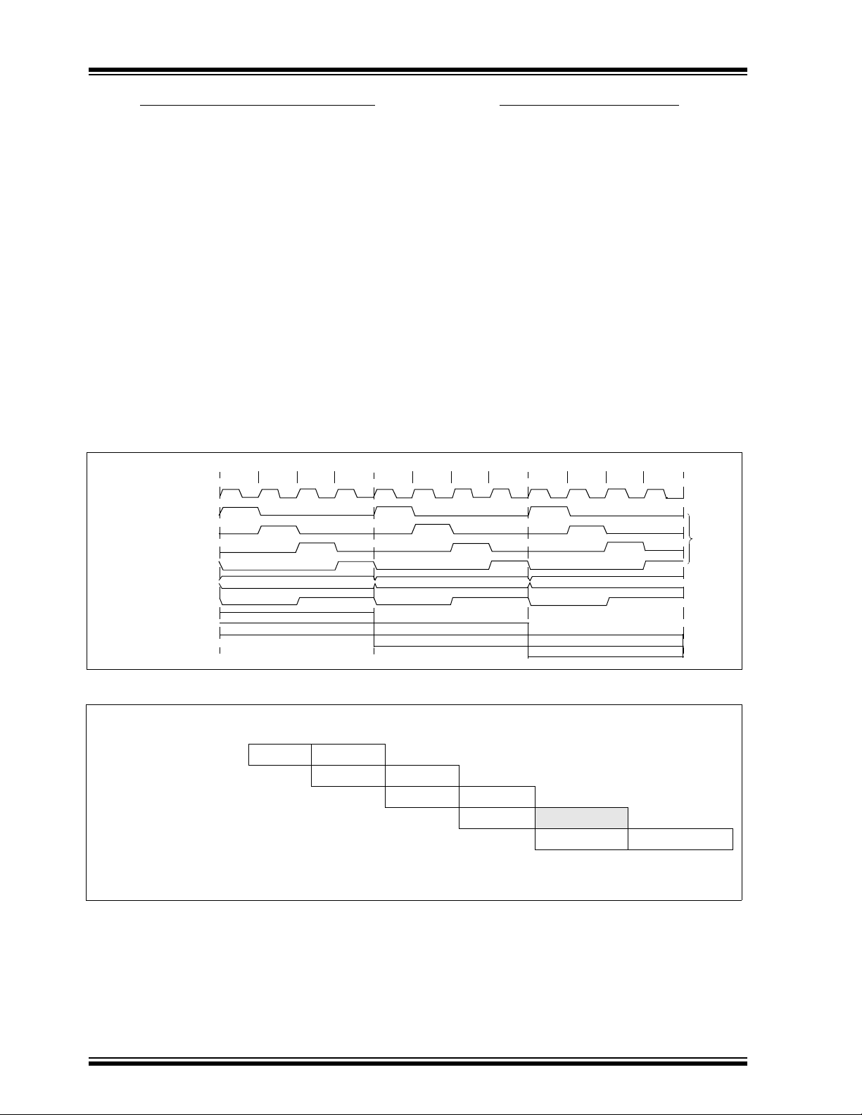
3.1 Clocking Scheme/Instruction Cycle
The clock input (from OSC1) is internally divided by
four to generate four non-overlapping quadrature
clocks, nam ely Q1, Q2, Q 3 and Q4. Int ernally, the program counter (PC) is incremented every Q1, and the
instruction is fetched from the program memory and
latched into the instruction register in Q4. The instruction is decoded and executed during the following Q1
through Q4. The clocks and instruction execution flow
is shown in Figure3-2.
FIGURE 3-2: CLOCK/INSTRUCTION CYCLE
Q2 Q3 Q4
Q1
OSC1
Q1
Q2
Q3
Q4
PC
OSC2/CLKOUT
(EXTRC and
INTRC modes)
PC PC+1 PC+2
Fetch INST (PC)
Execute INST (PC-1) Fetch INST (PC+1)
3.2 Instruction Flow/Pipelining
An “Instruction Cycle” consists of four Q cycles (Q1,
Q2, Q3 and Q4). The instruction fetch and execute
are pipelined such that fetch takes one instruction
cycle, while decode and execute takes another
instruction cycle. H owev er , due to the pipelining, each
instrn fetcveld 6xect ie onn tcytcls c-inanotheca4.8(ot)12.fhehe4e2xecouwı˝[()-042xech-2.6((g)12.5(e)]TJı˝0 -1.2267 TD2˝0.004[((i.e27.2 6))-02.1(.)]7Tı˝/F5 9.88 -101.22670.004[(GOT12.8( O02.1(.)]51.9(s)-3..8( O02.1(.)]1)]TJı˝0 8(cf)28.4(),12.8(ct)6(ng the)-25n,8( O02.1tw)18.6(o )13.3(cy)10(cl)12(es )13.3(are re)12.6(qu)-12(red)12.ng to TD2˝(42x)37(m)9.6(p2x)37(l)12(e2x)37(te)]TJı˝-4.5.226-1.2267 TD2˝0.0039 Tcı˝-0.0019 Twı˝[(the)13.2( in)13.2(str)-9.841.5˝028(h)-12x6(on )13.3((Exa.5˝028mp)13.2(le)-269.8c3-1).)]TJı˝0 -1.6667 TD2˝0.0036 Tcı˝0.0917 Twı˝[(A f)41.6(e2x)34(tc)10.3(h )13.3(cy)10.3(cl))9.3(e b)12.9(egi)12.3(ns)10.7(ew)5.6(i)-1.1(t)14.9(h2x)34( t)14.9(he )13.3(prog)39.07ca)12.9(m )13.3(co)12.9(unt)14.9(5to(Py)14.9(5tk-1.1(t)14.9.8(on C)h6n(Py)25˝09.6(( onn)13.4( )-2.976(t)8.3(cmy)-2(h)-12n)13.4()-12.9.6(( onn)g)-12nhe
Q2 Q3 Q4
Q1
Execute INST (PC) Fetch INST (PC+2)
Q2 Q3 Q4
Q1
Execute INST (PC+1)
Internal
phase
clock
EXAMPLE 3-1: INSTRUCTION PIPELINE FLOW
TCY0TCY1TCY2TCY3TCY4TCY5
1. MOVLW 55h
2. MOVWF GPIO
3. CALL SUB_1
4. BSF GPIO, BIT3 (Forced NOP)
5. Instruction @ address SUB_1
All instructions are single cycle, except for any program branches. These take two cycles since the fetched
instruction is “flushed” from the pipeline while the new instruction is being fetched and then executed.
DS30561B-page 10
Fetch 1 Execute 1
Fetch 2 Execute 2
Fetch 3 Execute 3
Fetch 4 Flush
Fetch SUB_1 Execute SUB_1
1999 Microchip Technology Inc.
PIC12C67X
4.0 MEMORY ORGANIZATION
4.1 Program Memory Organization
The PIC12C67X has a 13-b it p rog ram counter capa b l e
of addressing an 8K x 14 program memory space.
For the PIC12C671 and the PIC12CE673, the first 1K x
14 (0000h-03FFh) is implemented.
For the PIC12C672 and the PIC12CE674, the first 2K
x 14 (0000h-07FFh) is impl ement ed. Acc essing a loc ation above the physically implemented address will
cause a wraparound. The reset vector is at 0000h and
the interrupt vector is at 0004h.
FIGURE 4-1: PIC12C67X PROGRAM
MEMORY MAP AND STACK
PC<12:0>
CALL, RETURN
RETFIE, RETLW
Stack Level 1
Stack Level 8
13
4.2 Data Memory Organization
The data memory is partitioned into two banks, which
contain the Gener al Purpose Regist ers and the Special
Function Registers. Bit RP0 is the bank select bit.
RP0 (STATUS<5>) = 1 → Bank 1
RP0 (STATUS<5>) = 0 → Bank 0
Each Bank extends up to 7Fh (128 bytes). The lower
locations of each Bank are reserved for the Special
Function Registers . Abo v e the Spec ial Fun ction Re gisters are General Purpose Registers implemented as
static RAM. Both Bank 0 and Bank 1 contain Special
Function Re g is t ers. S o me " hig h u s e" S pecial Functi on
Registers fr om Bank 0 a re mir r ore d in Ba nk 1 for code
reduction and quicker access.
Also note that F0h through FFh on the PIC12C67X is
mapped into Bank 0 registers 70h-7Fh as common
RAM.
4.2.1 GENERAL PURPOSE REGISTER FILE
The register file can b e access ed eithe r dire ctly o r indi-
rectly through the File Select Register FSR
(Section 4.5).
Reset Vector
Peripheral
Interrupt Vector
On-Chip Program
Memory
(PIC12C672 and
PIC12CE674 only)
0000h
0004h
0005h
03FFh
0400h
07FFh
0800h
1FFFh
1999 Microchip Technology Inc. DS30561B-page 11
PIC12C67X
FIGURE 4-2: PIC12C67X REGISTER FILE
MAP
File
Address
00h
01h
02h
03h
04h
05h
06h
07h
08h
09h
0Ah
0Bh
0Ch
0Dh
0Eh
0Fh
10h
11h
12h
13h
14h
15h
16h
17h
18h
19h
1Ah
1Bh
1Ch
1Dh
1Eh
1Fh
20h
70h
7Fh
(1)
INDF
TMR0
PCL
STATUS
FSR
GPIO
PCLATH
INTCON
PIR1
ADRES
ADCON0
General
Purpose
Register
Bank 0 Bank 1
INDF
OPTION
PCL
STATUS
FSR
TRIS
PCLATH
INTCON
PIE1
PCON
OSCCAL
ADCON1
General
Purpose
Register
Mapped
in Bank 0
(1)
File
Address
80h
81h
82h
83h
84h
85h
86h
87h
88h
89h
8Ah
8Bh
8Ch
8Dh
8Eh
8Fh
90h
91h
92h
93h
94h
95h
96h
97h
98h
99h
9Ah
9Bh
9Ch
9Dh
9Eh
9Fh
A0h
BFh
C0h
EFh
F0h
FFh
4.2.2 SPECIAL FUNCTION REGISTERS
The Special Function Registers are registers used by
the CPU and Peripheral Modules for controlling the
desired operation of the device. These registers are
implemented as static RAM.
The Special Function Registers can be classified into
two sets (core and periphe ral). Those registers a ss oci-
ated with the “core” func tions are described in this section, and those related to the operation of the peripheral
features are described in the section of that peripheral
feature.
Unimplemented data memory locations, read
as ’0’.
Note 1: Not a physical register.
DS30561B-page 12
1999 Microchip Technology Inc.
PIC12C67X
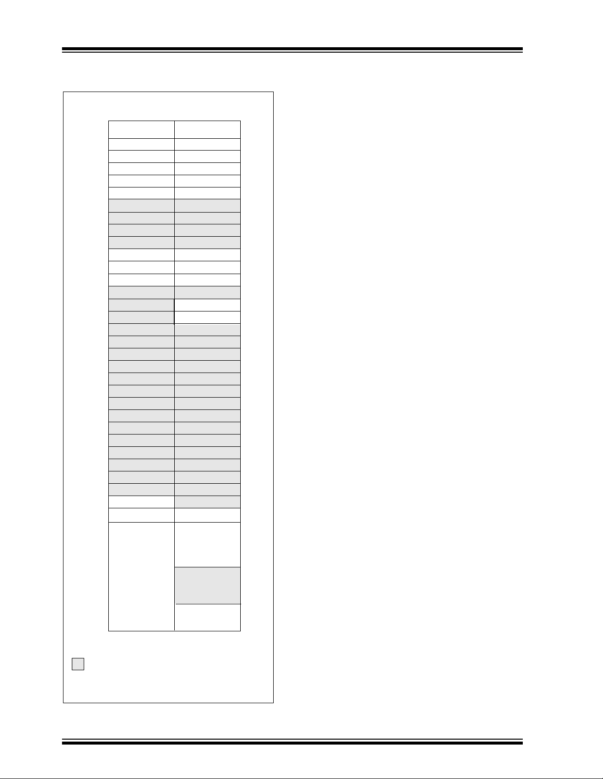
TABLE 4-1: PIC12C67X SPECIAL FUNCTION REGISTER SUMMARY
Address Name Bit 7 Bit 6 Bit 5 Bit 4 Bit 3 Bit 2 Bit 1 Bit 0
Value on
Power- on
Reset
Bank 0
(1)
00h
01h TMR0 Timer0 module’s register xxxx xxxx uuuu uuuu
02h
03h
04h
05h GPIO SCL
06h — Unimplemented — —
07h — Unimplemented — —
08h — Unimplemented — —
09h — Unimplemented — —
0Ah
0Bh
0Ch PIR1
0Dh — Unimplemented — —
0Eh — Unimplemented — —
0Fh — Unimplemented — —
10h — Unimplemented — —
11h — Unimplemented — —
12h — Unimplemented — —
13h — Unimplemented — —
14h — Unimplemented — —
15h — Unimplemented — —
16h — Unimplemented — —
17h — Unimplemented — —
18h — Unimplemented — —
19h — Unimplemented — —
1Ah — Unimplemented — —
1Bh — Unimplemented — —
1Ch — Unimplemented — —
1Dh — Unimplemented — —
1Eh ADRES A/D Result Register xxxx xxxx uuuu uuuu
1Fh ADCON0 ADCS1 ADCS0
INDF Addressing this location uses contents of FSR to address data memory (not a physical register) 0000 0000 0000 0000
(1)
PCL Program Counter's (PC) Least Significant Byte 0000 0000 0000 0000
(1)
STATUS IRP
(1)
FSR Indirect data memory address pointer xxxx xxxx uuuu uuuu
(1,2)
PCLATH — — — Write Buffer for the upper 5 bits of the Program Counter ---0 0000 ---0 0000
(1)
INTCON GIE PEIE T0IE INTE GPIE T0IF INTF GPIF 0000 000x 0000 000u
(4)
(5)
—ADIF— — — — — — -0-- ---- -0-- ----
RP1
SDA
(4)
RP0 TO PD ZDCC0001 1xxx 000q quuu
(5)
GP5 GP4 GP3 GP2 GP1 GP0 11xx xxxx 11uu uuuu
reserved CHS1 CHS0 GO/DO NE reserved ADON 0000 0000 0000 0000
Legend: x = unknown, u = unchanged, q = value depends on condition, - = unimplemented read as ’0’.
Shaded locations are unimplemented, read as ‘0’.
Note 1: These registers can be addressed from either bank.
2: The upper byte of the program counter is not directly accessible. PCLATH is a holding register for the PC<12:8> whose con-
tents are transferred to the upper byte of the program counter.
3: Other (non power-up) resets include external reset through MCLR
and Watchdog Timer Reset.
4: The IRP and RP1 bits are reserved on the PIC12C67X; always maintain these bits clear.
5: The SCL (GP7) and SDA (GP6) bits are unimplemented on the PIC12C671/672 and read as ’0’.
Value on
all other
Resets
(3)
1999 Microchip Technology Inc. DS30561B-page 13
PIC12C67X
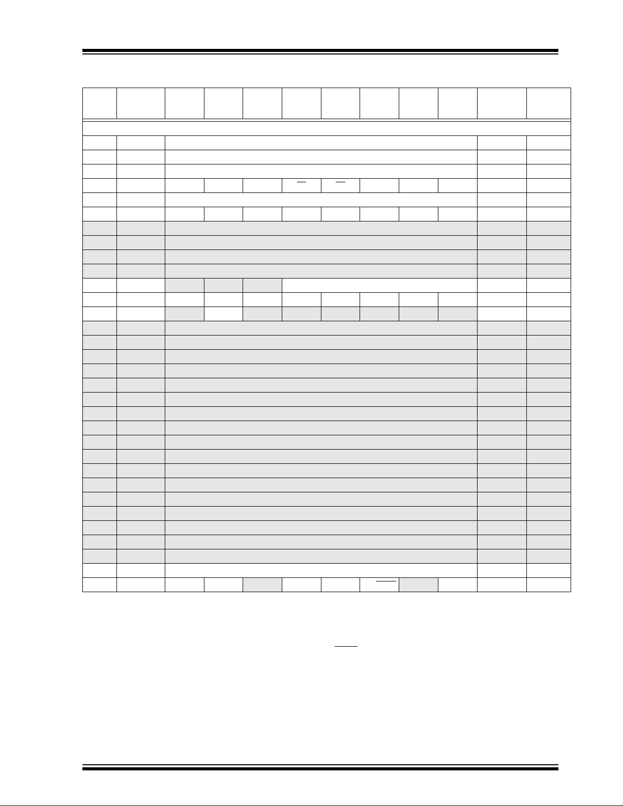
TABLE 4-1: PIC12C67X SPECIAL FUNCTION REGISTER SUMMARY (CONT.)
Address Name Bit 7 Bit 6 Bit 5 Bit 4 Bit 3 Bit 2 Bit 1 Bit 0
Bank 1
(1)
80h
81h OPTION GPPU
82h
83h
84h
85h TRIS
86h — Unimplemented — —
87h — Unimplemented — —
88h — Unimplemented — —
89h — Unimplemented — —
8Ah
8Bh
8Ch PIE1
8Dh — Unimplemented — —
8Eh PCON
8Fh OSCCAL CAL3 CAL2 CAL1 CAL0 CALFST CALSLW
90h — Unimplemented — —
91h — Unimplemented — —
92h — Unimplemented — —
93h — Unimplemented — —
94h — Unimplemented — —
95h — Unimplemented — —
96h — Unimplemented — —
97h — Unimplemented — —
98h — Unimplemented — —
99h — Unimplemented — —
9Ah — Unimplemented — —
9Bh — Unimplemented — —
9Ch — Unimplemented — —
9Dh — Unimplemented — —
9Eh — Unimplemented — —
9Fh ADCON1
INDF Addressing this location uses contents of FSR to address data memory (not a physical register) 0000 0000 0000 0000
INTEDG T0CS T0SE PSA PS2 PS1 PS0 1111 1111 1111 1111
(1)
PCL Program Counter’s (PC) Least Significant Byte 0000 0000 0000 0000
(1)
STATUS IRP
(1)
FSR Indirect data memory address pointer xxxx xxxx uuuu uuuu
(1,2)
PCLATH — — — Write Buffer for the upper 5 bits of the PC ---0 0000 ---0 0000
(1)
INTCON GIE PEIE T0IE INTE GPIE T0IF INTF GPIF 0000 000x 0000 000u
(4)
— — GPIO Data Direction Register --11 1111 --11 1111
—ADIE— — — — — — -0-- ---- -0-- ----
— — — — — —POR— ---- --0- ---- --u-
— — — — — PCFG2 PCFG1 PCFG0 ---- -000 ---- -000
RP1
(4)
RP0 TO PD ZDCC0001 1xxx 000q quuu
— — 0111 00-- uuuu uu--
Value on
Power- on
Reset
Legend: x = unknown, u = unchanged, q = value depends on condition, - = unimplemented read as ’0’.
Shaded locations are unimplemented, read as ‘0’.
Note 1: These registers can be addressed from either bank.
2: The upper byte of the program counter is not directly accessible. PCLATH is a holding register for the PC<12:8> whose con-
tents are transferred to the upper byte of the program counter.
3: Other (non power-up) resets include external reset through MCLR
and Watchdog Timer Reset.
4: The IRP and RP1 bits are reserved on the PIC12C67X; always maintain these bits clear.
5: The SCL (GP7) and SDA (GP6) bits are unimplemented on the PIC12C671/672 and read as ’0’.
Value on
all other
Resets
(3)
DS30561B-page 14
1999 Microchip Technology Inc.
PIC12C67X
4.2.2.1 STATUS REGISTER
The STA TUS R egist er, shown in Register 4-1, contains
the arithmetic status of th e ALU , the RE SET status an d
the bank select bits for data memory.
The STATUS Register can be the destination for any
instruction, as with any other register. If the STATUS
Register is the destina tion f or an instruction tha t aff ects
the Z, DC or C bits, then the write to these three bits is
disabled. The se bi ts ar e set or c leared accordi ng to the
device logic. Fur th er more, the TO
writable. Therefore, the result of an instruction with the
STATUS Register as destination may be different than
intended.
For example, CLRF STATUS will clear the upper three
bits and set the Z bit. This leaves the STATUS Register
as 000u u1uu (where u = unchanged).
and PD bits are not
It is recommended, therefore, that only BCF, BSF,
SWAPF and MOVWF instructions are used to alter the
STATUS Register, because these instructions do not
affect the Z, C or DC bi ts from the STATUS Register.
For other ins t ructi ons, not affe ct ing any status bi ts , see
the "Instruction Set Summary."
Note 1: Bits IRP and RP1 (STATUS<7:6>) are not
used by the PIC12C67X and should be
maintained clear. Use of these bits as
general purpose R/W bits is NOT recommended, since this may affect upward
compatibility with future products.
2: The C and DC bits operate as a borrow
and digit borrow bit, respectively, in subtraction. See the SUBLW and SUBWF
instructions for examples.
REGISTER 4-1: STATUS REGISTER (ADDRESS 03h, 83h)
Reserved Reserved R/W-0 R-1 R-1 R/W-x R/W-x R/W-x
IRP RP1 RP0 TO PD Z DC C R = Readable bit
bit7 bit0
bit 7: IRP: Register Bank Select bit (used for indirect addressing)
1 = Bank 2, 3 (100h - 1FFh)
0 = Bank 0, 1 (00h - FFh)
The IRP bit is reserved; always maintain this bit clear.
bit 6-5: RP<1:0>: Register Bank Select bits (used for direct addressing)
11 = Bank 3 (180h - 1FFh)
10 = Bank 2 (100h - 17Fh)
01 = Bank 1 (80h - FFh)
00 = Bank 0 (00h - 7Fh)
Each bank is 128 bytes. The RP1 bit is reserved; always maintain this bit clear.
bit 4: TO
bit 3: PD
bit 2: Z: Zero bit
bit 1: DC: Digit Carry/borrow
bit 0: C: Carry/borrow
: Time-out bit
1 = After power-up, CLRWDT instruction, or SLEEP instruction
0 = A WDT time-out occurred
: Power-down bit
1 = After power-up or by the CLRWDT inst ruction
0 = By execution of the SLEEP instruction
1 = The result of an arithmetic or logic operation is zero
0 = The result of an arithmetic or logic operation is not zero
bit (ADDWF, ADDLW,SUBLW,SUBWF instructions) (for borro w the pol arity is reversed)
1 = A carry-out from the 4th low order bit of the result occurred
0 = No carry-out from the 4th low order bit of the result
bit (ADDWF, ADDLW,SUBLW,SUBWF instructions)
1 = A carry-out from the most significant bit of the result occurred
0 = No carry-out from the most significant bit of the result occurred
W = Writable bit
U = Unimplemented bit,
- n = Value at POR reset
read as ‘0’
Note: For borrow
ond operand. For rotate (RRF, RLF) instructions, this bit is loaded with either the high or low order bit of
the source register.
1999 Microchip Technology Inc. DS30561B-page 15
the polarity is re v er sed. A subtr actio n is e x ec uted b y addi ng the tw o’s complement of the sec-

PIC12C67X
4.2.2.2 OPTION REGISTER
The OPTION Regi ster is a rea dab le a nd writabl e regi s-
ter, which contains various control bits to configure the
TMR0/WDT prescaler, the External INT Interrupt,
Note: To ac hieve a 1:1 prescaler as signmen t for
the TMR0 register, assign the prescaler to
the Watchdog Timer by setting bit PSA
(OPTION<3>).
TMR0 and the weak pull-ups on GPIO.
REGISTER 4-2: OPTION REGISTER (ADDRESS 81h)
R/W-1 R/W-1 R/W-1 R/W-1 R/W-1 R/W-1 R/W-1 R/W-1
GPPU
bit7 bit0
bit 7: GPPU: Weak Pull-up Enable
bit 6: INTEDG: Interrupt Edge
bit 5: T0CS: TMR0 Clock Source Select bit
bit 4: T0SE: TMR0 Source Edge Select bit
bit 3: PSA: Prescaler Assignment bit
bit 2-0: PS<2:0>: Prescaler Rate Select bits
INTEDG T0CS T0SE PSA PS2 PS1 PS 0 R = Readable bit
1 = Weak pull-ups disabled
0 = Weak pull-ups enabled (GP0, GP1, GP3)
1 = Interrupt on rising edge of GP2/T0CKI/AN2/INT pin
0 = Interrupt on falling edge of GP2/T0CKI/AN2/INT pin
1 = Transition on GP2/T0CKI/AN2/INT pin
0 = Internal instruction cycle clock (CLKOUT)
1 = Increment on high-to-low transition on GP2/T0CKI/AN2/INT pin
0 = Increment on low-to-high transition on GP2/T0CKI/AN2/INT pin
1 = Prescaler is assigned to the WDT
0 = Prescaler is assigned to the Timer0 module
Bit Value TMR0 Rate WDT Rate
000
001
010
011
100
101
110
111
1 : 2
1 : 4
1 : 8
1 : 16
1 : 32
1 : 64
1 : 128
1 : 256
1 : 1
1 : 2
1 : 4
1 : 8
1 : 16
1 : 32
1 : 64
1 : 128
W = Writable bit
U = Unimplemented bit,
read as ‘0’
- n = Value at POR reset
DS30561B-page 16
1999 Microchip Technology Inc.

PIC12C67X
4.2.2.3 INTCON REGISTER
The INTCON Regi ster i s a rea dab le a nd w ritabl e regi s-
ter, which contains various enable and flag bits for the
TMR0 Register overflow, GPIO port change and external GP2/INT pin interrupts.
Note: Interrupt flag bits get set when an in terrupt
condition occurs , re ga rdless of the state of
its corresponding enable bit or the global
enable bit, GIE (INTCON<7>).
REGISTER 4-3: INTCON REGISTER (ADDRESS 0Bh, 8Bh)
R/W-0 R/W-0 R/W-0 R/W-0 R/W-0 R/W-0 R/W-0 R/W-x
GIE PEIE T0IE INTE GPIE T0IF INTF GPIF R = Readable bit
bit7 bit0
bit 7: GIE: Global Interrupt Enabl e bit
1 = Enables all un-masked interrupts
0 = Disables all interrupts
bit 6: PEIE: Peripheral Interrupt Enable bit
1 = Enables all un-masked peripheral interrupts
0 = Disables all peripheral interrupts
bit 5: T0IE: TMR0 Overflow Interrupt Enable bit
1 = Enables the TMR0 interrupt
0 = Disables the TMR0 interrupt
bit 4: INTE: INT External Interrupt Enable bit
1 = Enables the external interrupt on GP2/INT/T0CKI/AN2 pin
0 = Disables the external interrupt on GP2/INT/T0CKI/AN2 pin
bit 3: GPIE: GPIO Interrupt on Change Enable bit
1 = Enables the GPIO Interrupt on Change
0 = Disables the GPIO Interrupt on Change
bit 2: T0IF: TMR0 Overflow Interrupt Flag bit
1 = TMR0 register has overflowed (must be cleared in software)
0 = TMR0 register did not overflow
bit 1: INTF: INT Exte rnal Interrupt Flag bit
1 = The external interrupt on GP2/INT/T0CKI/AN2 pin occurred (must be cleared in software)
0 = The external interrupt on GP2/INT/T0CKI/AN2 pin did not occur
bit 0: GPIF: GPIO Interrupt on Change Flag bit
1 = GP0, GP1 or GP3 pins changed state (must be cleared in software)
0 = Neither GP0, GP1 nor GP3 pins have changed state
W = Writable bit
U = Unimplemented bit,
- n = Value at POR reset
read as ‘0’
1999 Microchip Technology Inc. DS30561B-page 17

PIC12C67X
4.2.2.4 PIE1 REGISTER
This register contains the individual enable bits for the
Peripheral interrupts.
Note: Bit PEIE (INTCON<6>) must be set to
enable any peripheral interrupt.
REGISTER 4-4: PIE1 REGISTER (ADDRESS 8Ch)
U-0 R/W-0 U-0 U-0 U-0 U-0 U-0 U-0
—ADIE— — — — — — R = Readable bit
bit7 bit0
bit 7: Unimplemented: Read as ’0’
bit 6: ADIE: A/D Converter Interrupt Enable bit
1 = Enables the A/D interrupt
0 = Disables the A/D interrupt
bit 5-0: Unimplemented: Read as ’0’
W = Writable bit
U = Unimplemented bit,
- n = Value at POR reset
read as ‘0’
DS30561B-page 18
1999 Microchip Technology Inc.

PIC12C67X
4.2.2.5 PIR1 REGISTER
This register contains the individual flag bits for the
Peripheral interrupts.
Note: Interrupt flag bits get set when an in terrupt
condition occurs , re ga rdless of the state of
its corresponding enable bit or the global
enable bit, GIE (INTCON<7>). User software should ensure the appropriate interrupt flag bits are clear prior to enabling an
interrupt.
REGISTER 4-5: PIR1 REGISTER (ADDRESS 0Ch)
U-0 R/W-0 U-0 U-0 U-0 U-0 U-0 U-0
—ADIF— — — — — — R = Readable bit
bit7 bit0
bit 7: Unimplemented: Read as ’0’
bit 6: ADIF: A/D Converter Interrupt Flag bit
1 = An A/D conversion completed (must be cleared in software)
0 = The A/D conversion is not complete
bit 5-0: Unimplemented: Read as ’0’
W = Writable bit
U = Unimplemented bit,
- n = Value at POR reset
read as ‘0’
1999 Microchip Technology Inc. DS30561B-page 19
PIC12C67X
4.2.2.6 PCON REGISTER
The Power Control (PCON ) R eg ister contains a flag b it
to allow differentiation between a Power-on Reset
(POR), an external MCLR
REGISTER 4-6: PCON REGISTER (ADDRESS 8Eh)
U-0 U-0 U-0 U-0 U-0 U-0 R/W-0 U-0
— — — — — —POR— R = Readable bit
bit7 bit0
bit 7-2: Unimplemented: Read as ’0’
bit 1: POR
bit 0: Unimplemented: Read as ’0’
: Power-on Reset Status bit
1 = No Power-on Reset occurred
0 = A Power-on Reset occurred (must be set in software after a Power-on Reset occurs)
Reset and a WDT Reset.
W = Writable bit
U = Unimplemented bit,
- n = Value at POR reset
read as ‘0’
DS30561B-page 20
1999 Microchip Technology Inc.

4.2.2.7 OSCCAL REGISTER
The Oscillator Calibration (OSCCAL) Register is used
to calibrate the internal 4 MHz oscillator . It contains f our
bits for fine calibration and two other bits to either
increase or decrease frequency.
REGISTER 4-7: OSCCAL REGISTER (ADDRESS 8Fh)
R/W-0 R/W-1 R/W-1 R/W-1 R/W-0 R/W-0 U-0 U-0
CAL3 CAL2 CAL1 CAL0 CALFST CALSLW
bit7 bit0
bit 7-4: CAL<3:0>: Fine Calibration
bit 3: CALFST: Calibration Fast
1 = Increase frequency
0 = No change
bit 2: CALSLW: Calibration Slow
1 = Decrease frequency
0 = No change
bit 1-0: Unimplemented: Read as ’0’
— — R = Readable bit
PIC12C67X
W = Writable bit
U = Unimplemented bit,
read as ‘0’
- n = Value at POR reset
Note: If CALFST = 1 and CALSLW = 1, CALFST has precedence.
1999 Microchip Technology Inc. DS30561B-page 21
PIC12C67X
4.3 PCL and PCLATH
The Program Counter (PC) is 13-bits wide. The low
byte comes from the PC L Register, which is a readable
and writ able regi ster. The hi gh byte (PC< 12:8>) is no t
directly readable or wri table and comes from PCLATH.
On any reset, the PC is cleared. Figure 4-3 shows the
two situations for the loading of the PC. The upper
example in the figure shows how the PC is loaded on a
write to PCL (PCLA TH<4:0> → PCH). Th e low er e xample in the f igure shows how t he PC is loa ded dur ing a
CALL or GOTO instruction (PCLATH<4:3> → PCH).
FIGURE 4-3: LOADING OF PC IN
DIFFERENT SITUATIONS
PCH PCL
12 8 7 0
PC
PCLATH<4:0>
5
PCLATH
PCH PCL
12 11 10 0
PC
2
87
PCLATH
4.3.1 COMPUTED GOTO
11PCLATH<4:3>
8
Instruction with
PCL as
Destination
ALU result
GOTO, CALL
Opcode <10:0>
4.3.2 STAC K
The PIC12C67X family has an 8-level deep x 13-bit
wide hardware stack. The stack space is not par t of
either program or data space and the stack pointer is
not readable or writable. The PC is PUSHed onto the
stack when a CALL instruction is executed or an in terrupt caus es a branch. The s tack is POPed in the event
of a RETURN, RETLW or a RETFIE instruction execution. PCLATH is not affected by a PUSH or POP operation.
The stack oper ates as a circular buff er . This means that
after the stack has been PUSHed eigh t time s, the n inth
push ov erwrites th e value that was stored from the firs t
push. The tenth push overwrites the sec ond pus h (an d
so on).
Note 1: There are no status bits to indicate stack
overflow or stack underflow conditions.
2: There are no instructions/mnemonics
called PUSH or POP. These are actions
that occur from the execution of the
CALL, RETURN, RETLW, and RETFIE
instructions, or the vectoring to an interrupt address.
4.4 Program Memory Paging
The PIC12C67X ignores both paging bits
PCLATH<4:3>, which are used to access program
memory when more than one page is available. The
use of PCLATH<4:3> as general purpose read/write
bits for the PIC12C67X is not recommended since this
may affect upward compatibility with future products.
A Computed GOTO is accomplished by adding an offset to the program counter (ADDWF PCL). When doing
a table read using a computed GOTO method, care
should be exercised i f the table location crosses a PCL
memory boundary (each 256 byte block). Refer to the
application note
“Implementing a Table Read"
(AN556).
DS30561B-page 22
1999 Microchip Technology Inc.

PIC12C67X
4.5 Indirect Addressing, INDF and FSR Registers
The INDF Register is not a physical register. Addressing the INDF Register will cause indirect addressing.
Any instruction using the INDF register actually
accesses the register p ointed to b y the File Sele ct Register, FSR. Reading the INDF Register itself indirectly
(FSR = ’0’) will read 00h. Writing to the INDF Register
indirectly results in a no-o per atio n (althou gh statu s bits
may be affected). An effective 9-bit addres s is obta ined
by concatenati ng the 8-bit FSR Register a nd the IRP bit
(STA TUS<7>), as shown in Figure 4-4. Howev er , IRP is
not used in the PIC12C67X.
A simple program to clear RAM locations 20h-2Fh
using indirect addressing is shown in Example 4-1.
FIGURE 4-4: DIRECT/INDIRECT ADDRESSING
RP1 RP0
(1)
6
from opcode
0
EXAMPLE 4-1: INDIR ECT ADDRESSING
movlw 0x20 ;initialize pointer
movwf FSR ;to RAM
NEXT clrf INDF ;clear INDF register
incf FSR,F ;inc pointer
btfss FSR,4 ;all done?
goto NEXT ;no clear next
CONTINUE
: ;yes continue
Indirect AddressingDirect Addressing
(1)
IRP
7
FSR register
0
bank select location select
00 01 10 11
00h
not used
Data
Memory
7Fh
Bank 0 Bank 1 Bank 2 Bank 3
For register file map detail see Figure 4-2.
Note 1: The RP1 and IRP bits are reserved; always maintain these bits clear.
bank select
180h
1FFh
location select
1999 Microchip Technology Inc. DS30561B-page 23

PIC12C67X
NOTES:
DS30561B-page 24
1999 Microchip Technology Inc.

PIC12C67X
5.0 I/O PORT
As with any other register, the I/O register can be
written and read under pr ogr am c ontrol. How e ver, read
instructi ons (i.e., MOVF GPIO,W) always read the I/O
pins independent of the pin’s input/output modes. On
RESET, all I/O ports are defined as input (inputs are at
hi-impedance), since the I/O control registers are all
set.
5.1 GPIO
GPIO is an 8-bit I/O register. Only the low order 6 bits
are used (GP<5:0>). Bits 6 and 7 (SDA and SCL,
respectively) are used by the EEPROM peripheral on
the PIC12CE673/674. Refer to Section 6.0 and
Appendix B for use of SDA and SCL. Please note that
GP3 is an input only pin. The configuration word can
set several I/O’s to alternate functions. When acting as
alternate functions, the pins will read as ‘0’ during port
read. Pins GP0, GP1 and GP3 can be configured with
weak pull-ups and also with interrupt-on-change. The
interrupt on change and w e ak pul l-u p fu nc tion s a r e n ot
pin selectable. If pin 4, (GP3), is configured as MCLR
a weak pull-up is always on. Interrupt-on-change for
this pin is not se t and GP3 will read a s ' 0'. I nterrupt-o nchange is enabled by setting bit GPIE, INTCON<3>.
Note that external oscillator use overrides the GPIO
functions on GP4 and GP5.
5.3 I/O Interfacing
The equivalent circuit for an I/O port pin is shown in
Figure 5-1 through Figure 5-5. All port pins, except
GP3, which is input only, may be used for both input
and output operations. For input operations, these
ports are non-latching. Any input must be present until
read by an input instruction (i.e., MOVF GPIO,W). The
outputs are latched and remain unchanged until the
output lat ch is rewritte n. To use a port pi n as output,
the corresponding direc ti on c ontrol bit in TRIS must be
cleared (= 0). For use as an input, the corresponding
TRIS bit must be set. Any I/O pin (except GP3) can be
programmed individually as input or output.
Port pins GP6 (SDA) and GP7 (SCL) are used for the
serial EEPROM interface on the PIC12CE673/674.
These port pins are not available externally on the
package. Users should avoid writing to pins GP6
(SDA) and GP7 (SCL) when not communicating with
the serial EEPROM memory. Please see Section 6.0,
EEPROM Peripheral Operation, for information on
serial EEPROM communication.
,
Note: On a Power-on Reset, GP0, GP1, GP2
and GP4 are configured as analog inputs
and read as '0'.
5.2 TRIS Register
This register controls the data direction for GPIO. A '1'
from a TRIS Register bit p uts the correspo nding o utput
driver in a hi-impedance mode. A '0' puts the contents
of the output data latch on the selected pins, enabling
the output buffer. The exceptions are GP3, which is
input only and its TRIS bit will always read as '1', while
GP6 and GP7 TRIS bits will read as ’0’.
Note: A read of the ports reads the pins, not the
output data latches. That is, if an output
driver on a pin is enabled and driven high,
but the external system is holding it low, a
read of the p o rt will i n di cat e t h a t th e pi n i s
low.
Upon reset, the TRIS Register is all '1's, making all
pins inputs.
TRIS for pins GP4 and GP5 is forced to a ’1’ where
appropriate. Writes to TRIS <5:4> will have an effect
in EXTRC and INTRC oscillator modes only. When
GP4 is configured as CLKOUT, changes to TRIS<4>
will have no effect.
1999 Microchip Technology Inc. DS30561B-page 25
PIC12C67X
FIGURE 5-1: BLOCK DIAGRAM OF GP0/AN0 AND GP1/AN1/VREF PIN
GPPU
Data Bus
WR PORT
WR TRIS
DQ
CK
Data Latch
DQ
CK
TRIS Latch
GP0/INT
Q
Q
RD PORT
(1)
and GP1/INT
RD TRIS
(1)
V
DD
P
N
VSS
Analog
Input
Mode
DQ
EN
VDD
P
TTL
Input
Buffer
VDD
I/O Pin
VSS
To A/D Converter
Note 1: Wake-up on pin change interrupts for GP0 and GP1.
DS30561B-page 26
1999 Microchip Technology Inc.
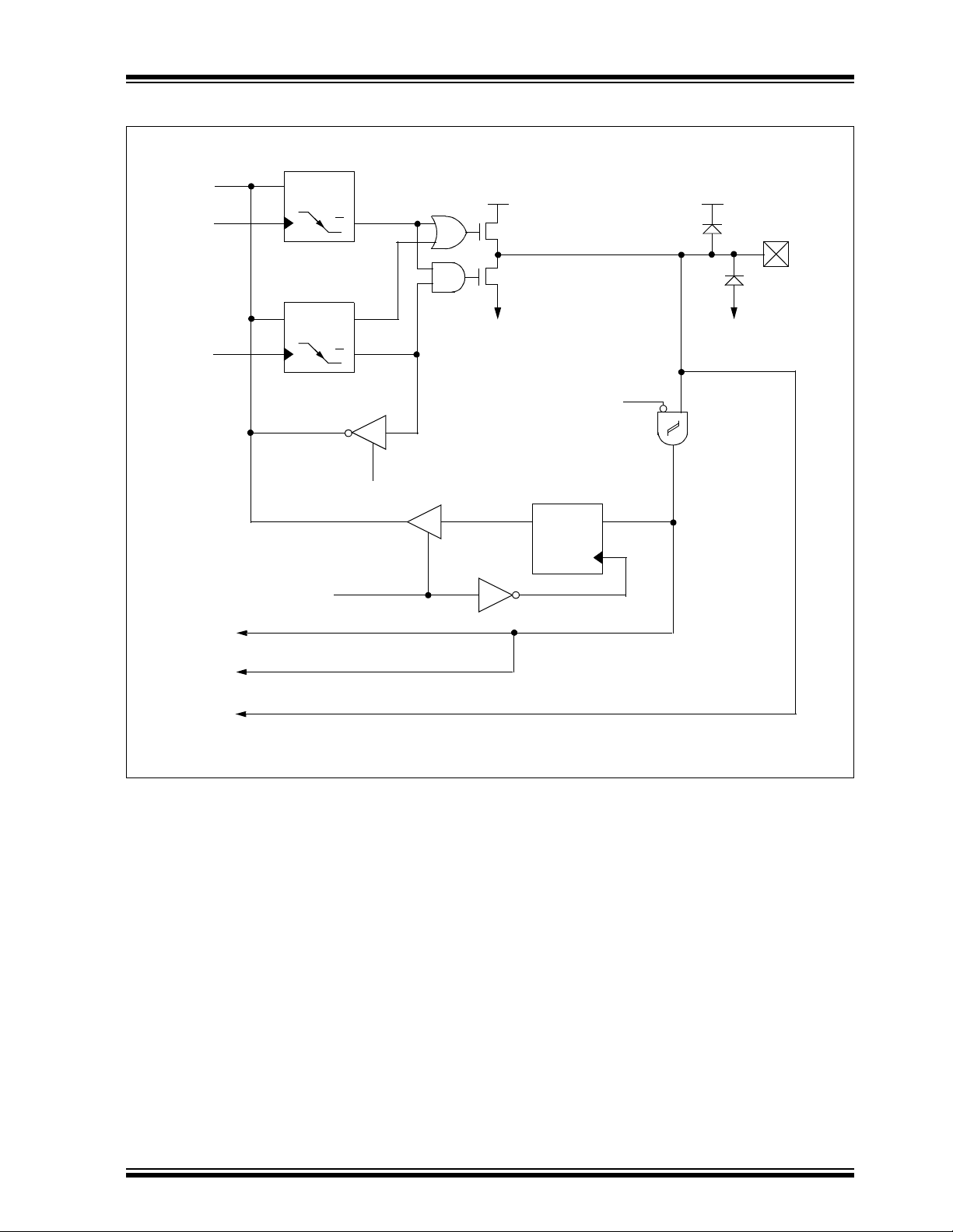
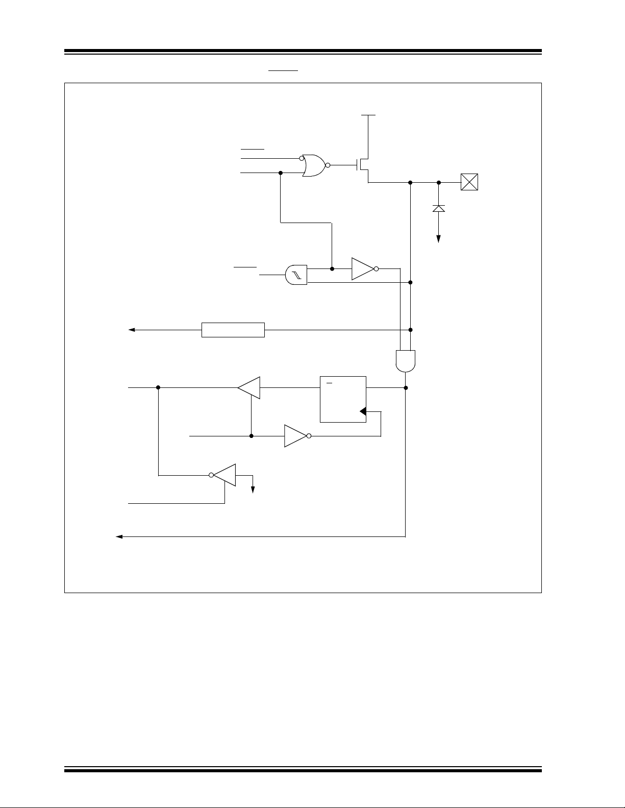
FIGURE 5-2: BLOCK DIAGRAM OF GP2/T0CKI/AN2/INT PIN
PIC12C67X
Data Bus
WR PORT
WR TRIS
DQ
CK
Q
Data Latch
DQ
CK
Q
TRIS Latch
RD PORT
TMR0 Clock Input
RD TRIS
V
DD
P
N
V
SS
Analog
Input
Mode
DQ
EN
VDD
I/O Pin
VSS
Schmitt Tr igger
Input Buffer
GP2/INT
To A/D Conver ter
1999 Microchip Technology Inc. DS30561B-page 27
PIC12C67X
FIGURE 5-3: BLOCK DIAGRAM OF GP3/MCLR/VPP PIN
GPPU
MCLREN
MCLR
Schmitt Trigger
Input Buffer
VDD
P
Input Pin
VSS
Program Mode
Data Bus
RD TRIS
GP3/INT
Note 1: Wake-up on pin change interrupt for GP3.
(1)
HV Detect
RD PORT
SS
V
TTL Input
Buffer
DQ
EN
DS30561B-page 28
1999 Microchip Technology Inc.
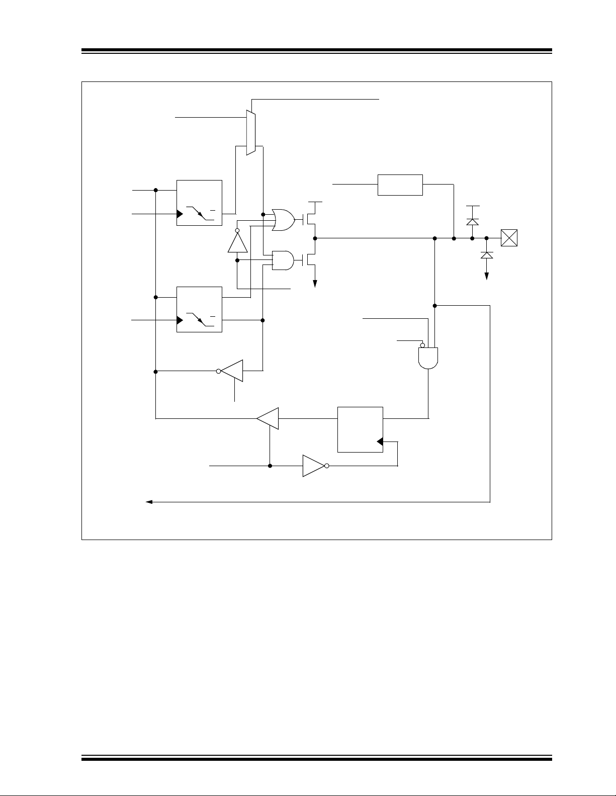
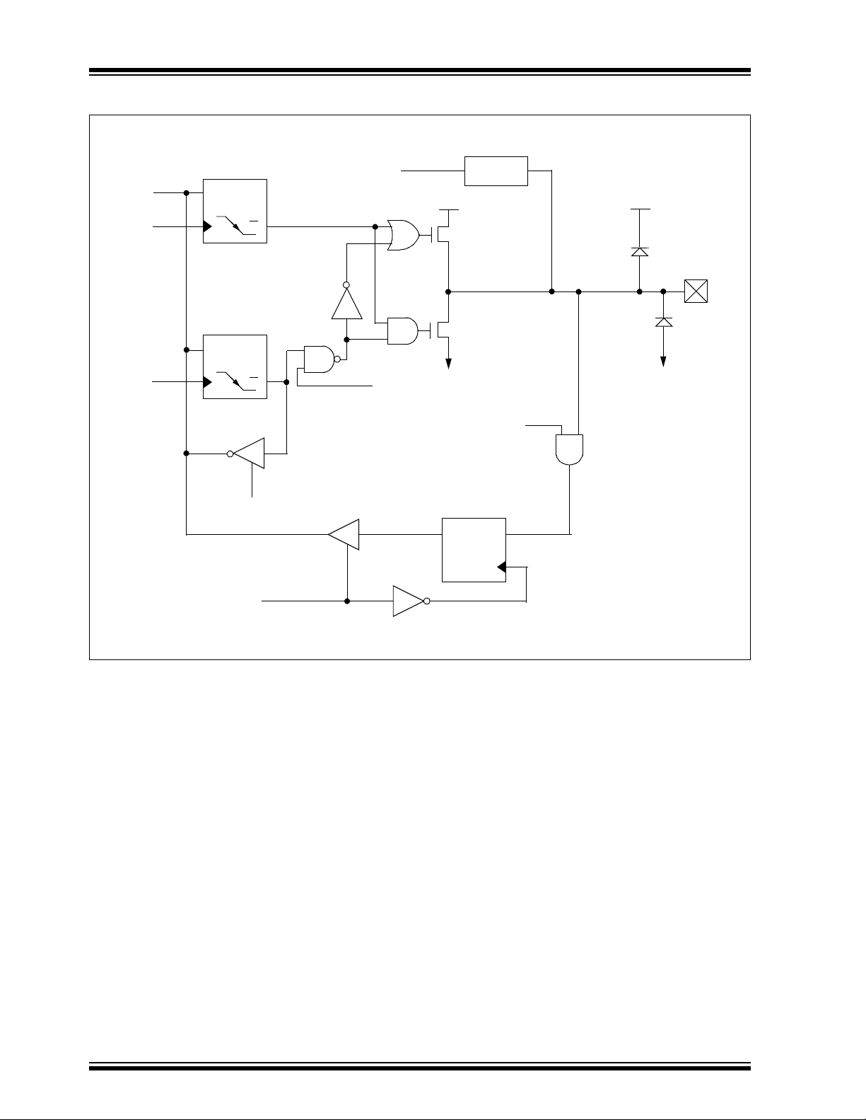
FIGURE 5-4: BLOCK DIAGRAM OF GP4/OSC2/AN3/CLKOUT PIN
PIC12C67X
Data Bus
WR PORT
WR TRIS
CLKOUT (F
DQ
CK
Q
Data Latch
DQ
CK
Q
TRIS Latch
OSC/4)
INTRC or EXTRC w/ CLKOUT
1
0
V
DD
P
N
INTRC/
EXTRC
VSS
From OSC1
INTRC or EXTRC
w/o CLKOUT
Oscillator
Circuit
Analog
Input
Mode
VDD
TTL
Input Buffer
I/O Pin
VSS
RD PORT
To A/D Converter
RD TRIS
DQ
EN
1999 Microchip Technology Inc. DS30561B-page 29
PIC12C67X
FIGURE 5-5: BLOCK DIAGRAM OF GP5/OSC1/CLKIN PIN
Data Bus
WR PORT
WR TRIS
DQ
EN
Q
Data Latch
DQ
EN
Q
TRIS Latch
RD TRIS
INTRC
To OSC2
Oscillator
Circuit
V
DD
P
N
VSS VSS
INTRC
DQ
EN
VDD
TTL
Input Buffer
I/O Pin
RD PORT
DS30561B-page 30
1999 Microchip Technology Inc.
 Loading...