

Datasheet PIC10F220, PIC10F222 Datasheet

PIC10F220/222
Data Sheet
High-Performance Microcontrollers
with 8-bit A/D
© 2007 Microchip Technology Inc. DS41270E

Note the following details of the code protection feature on Microchip devices:
• Microchip products meet the specification contained in their particular Microchip Data Sheet.
• Microchip believes that its family of products is one of the most secure families of its kind on the market today, when used in the
intended manner and under normal conditions.
• There are dishonest and possibly illegal methods used to breach the code protection feature. All of these methods, to our
knowledge, require using the Microchip products in a manner outside the operating specifications contained in Microchip’s Data
Sheets. Most likely, the person doing so is engaged in theft of intellectual property.
• Microchip is willing to work with the customer who is concerned about the integrity of their code.
• Neither Microchip nor any other semiconductor manufacturer can guarantee the security of their code. Code protection does not
mean that we are guaranteeing the product as “unbreakable.”
Code protection is constantly evolving. We at Microchip are committed to continuously improving the code protection features of our
products. Attempts to break Microchip’s code protection feature may be a violation of the Digital Millennium Copyright Act. If such acts
allow unauthorized access to your software or other copyrighted work, you may have a right to sue for relief under that Act.
Information contained in this publication regarding device
applications and t he lik e is provided only for your convenience
and may be su perseded by upda t es . It is y our responsibility to
ensure that your application meets with your specifications.
MICROCHIP MAKES NO REPRESENTATIONS OR
WARRANTIES OF ANY KIND WHETHER EXPRESS OR
IMPLIED, WRITTEN OR ORAL, STATUTORY OR
OTHERWISE, RELATED TO THE INFORMATION,
INCLUDING BUT NOT LIMITED TO ITS CONDITION,
QUALITY, PERFORMANCE, MERCHANTABILITY OR
FITNESS FOR PURPOSE. Microchip disclaims all liability
arising from this information and its use. Use of Microchip
devices in life supp ort and/or safety ap plications is entir ely at
the buyer’s risk, and the buyer agrees to defend, indemnify and
hold harmless M icrochip from any and all dama ges, claims,
suits, or expenses re sulting from such use. No licens es are
conveyed, implicitly or otherwise, under any Microchip
intellectual property rights.
Trademarks
The Microchip name and logo, the Microchip logo, Accuron,
dsPIC, K
EELOQ, KEELOQ logo, microID, MPLAB, PIC,
PICmicro, PICSTART, PROMATE, rfPIC and SmartShunt are
registered trademarks of Microchip Technology Incorporated
in the U.S.A. and other countries.
AmpLab, FilterLab, Linear Active Thermistor, Migratable
Memory, MXDEV, MXLAB, SEEVAL, SmartSensor and The
Embedded Control Solutions Company are registered
trademarks of Microchip Technology Incorporated in the
U.S.A.
Analog-for-the-Digital Age, Application Maestro, CodeGuard,
dsPICDEM, dsPICDEM.net, dsPICworks, dsSPEAK, ECAN,
ECONOMONITOR, FanSense, FlexROM, fuzzyLAB,
In-Circuit Serial Programming, ICSP, ICEPIC, Mindi, MiWi,
MPASM, MPLAB Certified logo, MPLIB, MPLINK, PICkit,
PICDEM, PICDEM.net, PICLAB, PICtail, PowerCal,
PowerInfo, PowerMate, PowerTool, REAL ICE, rfLAB, Select
Mode, Smart Serial, SmartTel, Total Endurance, UNI/O,
WiperLock and ZENA are trademarks of Microchip
Technology Incorporated in the U.S.A. and other countries.
SQTP is a service mark of Microchip Technology Incorporated
in the U.S.A.
All other trademarks mentioned herein are property of their
respective companies.
© 2007, Microchip Technology Incorporated, Printed in the
U.S.A., All Rights Reserved.
Printed on recycled paper.
Microchip received ISO/TS-16949:2002 certification for its worldwide
headquarters, design and wafer fabrication facilities in Chandler and
Tempe, Arizona; Gresham, Oregon and design centers in California
and India. The Company’s quality system processes and procedures
are for its PIC
devices, Serial EEPROMs, microperipherals, nonvolatile memory and
analog products. In addition, Microchip’s quality system for the design
and manufacture of development systems is ISO 9001:2000 certified.
®
MCUs and dsPIC® DSCs, KEELOQ
®
code hopping
DS41270E-page ii © 2007 Microchip Technology Inc.

PIC10F220/222
6-Pin, 8-Bit Flash Microcontrollers
Device Included In This Data Sheet:
•PIC10F220
•PIC10F222
High-Performance RISC CPU:
• Only 33 Single-Word Instructions to Learn
• All Single-Cycle Instructions Except for Program
Branches which are Two-Cycle
• 12-bit Wide Instructions
• 2-Level Deep Hardware Stack
• Direct, Indirect and Relative Addressing modes
for Data and Instructions
• 8-bit Wide Data Path
• 8 Special Function Hardware Registers
• Operating Speed:
- 500 ns instruction cycle with 8 MHz internal
clock
-1μs instruction cycle with 4 MHz internal
clock
Special Microcontroller Features:
• 4 or 8 MHz Precision Internal Oscillator:
- Factory calibrated to ±1%
• In-Circuit Serial Programming™ (ICSP™)
• In-Circuit Debugging (ICD) Support
• Power-On Reset (POR)
• Short Device Reset Timer, DRT (1.125 ms typical)
• Watchdog Timer (WDT) with Dedicated On-Chip
RC Oscillator for Reliable Operation
• Programmable Code Protection
• Multiplexed MCLR
• Internal Weak Pull-Ups on I/O Pins
• Power-Saving Sleep mode
• Wake-up from Sleep on Pin Change
Input Pin
Low-Power Features/CMOS Technology:
• Operating Current:
-< 175μA @ 2V, 4 MHz
• Standby Current:
- 100 nA @ 2V, typical
• Low-Power, High-Speed Flash Technology:
- 100,000 Flash endurance
- > 40-year retention
• Fully Static Design
• Wide Operating Voltage Range: 2.0V to 5.5V
• Wide Temperature Range:
- Industrial: -40°C to +85°C
- Extended: -40°C to +125°C
Peripheral Features:
• 4 I/O Pins:
- 3 I/O pins with individual direction control
- 1 input only pin
- High current sink/source for direct LED drive
- Wake-on-change
- Weak pull-ups
• 8-bit Real-Time Clock/Counter (TMR0) with 8-bit
Programmable Prescaler
• Analog-to-Digital (A/D) Converter:
- 8-bit resolution
- 2 external input channels
- 1 internal input channel dedicated
Device
PIC10F220 256 16 4 1 2
PIC10F222 512 23 4 1 2
© 2007 Microchip Technology Inc. DS41270E-page 1
Program Memory Data Memory
I/O
Flash (words) SRAM (bytes)
Timers
8-bit
8-Bit A/D (ch)

PIC10F220/222
PIC10F220/222
1
2
3
6
5
4
GP0/AN0/ICSPDAT
V
SS
GP1/AN1/ICSPCLK
GP3/MCLR/VPP
VDD
GP2/T0CKI/FOSC4
GP2/T0CKI/FOSC4
N/C
N/C
PIC10F220/222
1
2
3
4
8
7
6
5
VDD
GP3/MCLR/VPP
VSS
GP0/AN0/ICSPDAT
GP1/AN1/ICSPCLK
N/C
GP3/MCLR/VPP
VSS
GP0/AN0/ICSPDAT
N/C
GP2/T0CKI/FOSC4
VDD
GP1/AN1/ICSPCLK
1
2
3
4
8
7
6
5
PIC10F220/222
6-Lead SOT-23 Pin Diagram
8-Lead DIP Pin Diagram
8-Lead DFN Pin Diagram
DS41270E-page 2 © 2007 Microchip Technology Inc.

PIC10F220/222
Table of Contents
1.0 General Description............................................................................................. .... .. ...... ............................................................. 5
2.0 Device Varieties .......................................................................................................................................................................... 7
3.0 Architectural Overview................................................................................................................................................................. 9
4.0 Memory Organization................................................................................................................................................................. 13
5.0 I/O Port............................................. .................................................. ........................................................................................21
6.0 TMR0 Module and TMR0 Register............................................................................................................................................. 25
7.0 Analog-to-Digital (A/D) converter ............................................................................................................................................... 29
8.0 Special Features Of The CPU....................................................................... ............................................................................. 33
9.0 Instruction Set Summary............................................................................................................................................................ 43
10.0 Electrical Characteristics............................................................................................................................................................ 51
11.0 Development Support................................................................................................................................................................. 61
12.0 DC and AC Characteristics Graphs and Charts......................................................................................................................... 69
13.0 Packaging Information. .................................................. .............................................................................................................73
Index .................................................................................................................................................................................................... 79
The Microchip Web Site.............. ................................................... ......................... ............................................................................. 81
Customer Change Notification Service ................................................................................................................................................ 81
Customer Support................................................................................................................................................................................ 81
Reader Response................................................................................................................................................................................ 82
Product Identification System .............................................................................................................................................................. 83
TO OUR VALUED CUSTOMERS
It is our intention to provide our valued customers with the best documentation possible to ensure successful use of your
Microchip products. To this end, we will continue to improve our publications to better suit your needs. Our publications will be
refined and enhanced as new volumes and updates are introduced.
If you have any questions or comments regarding this publication, please contact the Market ing Com munica tions D epartment via
E-mail at docerrors@mail.microchip.com or fax the Reader Response Form in the back of this data sheet to (480) 792-4150.
We welcome your feedback.
Most Current Data Sheet
To obtain the most up-to-date version of this data sheet, please register at our Worldwide Web site at:
http://www.microchip.com
You can determine the version of a data sheet by examining its literature number found on the bottom outside corner of any page.
The last character of the literature number is the version number, (e.g., DS30000A is version A of document DS30000).
Errata
An errata sheet, describing minor operational differences from the data sheet and recommended workarounds, may exist for current
devices. As device/documentation issues become known to us, we will publish an errata sheet. The errata will spec ify the revision
of silicon and revision of document to which it applies.
To determine if an errata sheet exists for a particular device, please check with one of the following:
• Microchip’s Worldwide Web site; http://www.microchip.com
• Your local Microchip sales office (see last page)
• The Microchip Corporate Literature Center; U.S. FAX: (480) 792-7277
When contacting a sales office or the literature center, please specify which device, revision of silicon and data sheet (include
_literature number) you are using.
Customer Notification System
Register on our web site at www.microchip.com/cn to receive the most current information on all of our products.
© 2007 Microchip Technology Inc. DS41270E- page 3

PIC10F220/222
NOTES:
DS41270E-page 4 © 2007 Microchip Technology Inc.

PIC10F220/222
1.0 GENERAL DESCRIPTION
The PIC10F220/222 devices from Microchip
T ec hnology are lo w-cost, hig h-performance , 8-bit, fullystatic Flash-based CMOS microcontrollers. They
employ a RISC architecture with only 33 single-word/
single-cycle instructions. All instructions are singlecycle (1 μs) except for program branches, which take
two cycles. The PIC 10F220/22 2 devices deliver performance in an order of mag nitu de h igh er th an t hei r com petitors in the same price category. The 12-bit wide
instructions are highly symmetrical, resulting in a
typical 2:1 code compression over other 8-bit
microcontrollers in its class. The easy-to-use and easy
to remember instruction set reduces development time
significantly.
The PIC10F220/222 products are equipped with special features that reduce system cost and power
requirements. The Power-on Reset (POR) and Device
Reset Ti mer (DR T) e limin ates the ne ed fo r the externa l
Reset circuitry . INT OSC Internal Oscillator m ode is provided, thereby, preserving the limited number of I/O
available. Power-Sav ing Sle ep mode, Watchdog Timer
and code protection features improve system cost,
power and reliability.
The PIC10F220/222 devices are available in costeffective Flash, which is suitable for production in any
volume. The customer can take full advantage of
Microchip’s price leadership in Flash programmable
microcontrollers while benefiting from the Flash
programmable flexibility.
The PIC10F220/222 products are supported by a fullfeatured macro assembler, a software simulator, an incircuit debugger, a ‘C’ compiler, a low-cost
development programmer and a full featured programmer. All the tools are supported on IBM
compatible machines.
®
PC and
1.1 Applications
The PIC10F220/222 devices fit in applications ranging
from personal care app li anc es an d s ecu rity s ys tem s to
low-power remote transmitters/receivers. The Flash
technology makes customizing application programs
(transmitter codes, appliance settings, receiver frequencies, etc.) extremely fast and convenient. The
small footprint packages, for through hole or surface
mounting, make th ese micr ocontroll ers wel l suited for
applications with space limitations. Low-cost, lowpower, high-performance, ease-of-use and I/O flexibility make the PIC10F220/222 devices very versatile,
even in areas where no microcontroller use has been
considered before (e.g., timer functions, logic and
PLDs in larger system s and co processor applications).
T ABLE 1-1: PIC10F220/222 DEVICES
Clock Maximum Frequency of Operation (MHz) 8 8
Memory Flash Program Memory 256 512
Data Memory (bytes) 16 23
Peripherals Timer Module(s) TMR0 TMR0
Wake-up from Sleep on pin change Yes Yes
Analog inputs 2 2
Features I/O Pins 3 3
Input Only Pins 1 1
Internal Pull-ups Yes Yes
In-Circuit Serial Programming™ Ye s Yes
Number of instructions 33 33
Packages 6-pin SOT-23,
Note 1: The PIC10F220/222 devices have Power-on Reset, selectable Watchdog Timer, selectable code-protect, high I/O
current capability and precision internal oscillator.
2: The PIC10F220/222 devices use serial programming with data pin GP0 and clock pin GP1.
© 2007 Microchip Technology Inc. DS41270E-page 5
(1), (2)
PIC10F220 PIC10F222
8-pin DIP, DFN
6-pin SOT-23,
8-pin DIP, DFN

PIC10F220/222
NOTES:
DS41270E-page 6 © 2007 Microchip Technology Inc.

2.0 DEVICE VARIETIES
A variety of packaging options are available. Depending on application and production requirements, the
proper device option can be selected using the
information in th is section. Wh en placing orde rs, please
use the PIC10F220/222 Product Identification System
at the back of this data s heet to s pecify the correct p art
number.
2.1 Quick Turn Programming (QTP) Devices
Microchip offers a QTP programming service for
factory production orders. This service is made
available for users who choose not to program
medium-to-high quantity units and whose code
patterns have stabilized. The devices are identical to
the Flash devices but with all Flash locations and fuse
options already programmed by the factory. Certain
code and prototype verification procedures do apply
before production shipments are available. Please
contact your loc al Microchi p Technology sales off ice for
more details.
PIC10F220/222
2.2 Serialized Quick Turn
Programming
Microchip offers a unique programming service, where
a few user-defined locations in each device are
programmed with different serial numbers. The serial
numbers may be random, pseudo-random or
sequential.
Serial programming allows each device to have a
unique number, which can serve as an entry-code,
password or ID number.
SM
(SQTPSM) Devices
© 2007 Microchip Technology Inc. DS41270E-page 7

PIC10F220/222
NOTES:
DS41270E-page 8 © 2007 Microchip Technology Inc.

PIC10F220/222
3.0 ARCHITECTURAL OVERVIEW
The high performance of the PIC10F220/222 devices
can be attributed to a number of architectural features
commonly found in RISC microprocessors. To begin
with, the PIC10F220/222 devices use a Harvard architecture in which program and data are accessed on
separate buses. This improves bandwidth over traditional von Neumann architectures where program and
data are fetch ed on the sa me bu s. Sep arating progra m
and data memor y further allow s instructions to be sized
differently than the 8-bit wide data word. Instruction
opcodes are 12 bit s wide, making it p ossible to have all
single-word instructions. A 12-bit wide program memory access bus fetches a 12-bit instruction in a single
cycle. A two-stage pipeline overlaps fetch and execution of instructions. Consequently, all instructions (33)
execute in a single cycle (1 μs @ 4 MHz or 500 ns @
8 MHz) except for program branches.
The table belo w lists p rogram me mory (Flash) and data
memory (RAM) for the PIC10F220/222 devices.
Memory
Device
Program Data
PIC10F220 256 x 12 16 x 8
PIC10F222 512 x 12 23 x 8
The PIC10F220/222 devices contain an 8-bit ALU and
working register. The ALU is a general purpose arithmetic unit. It performs arithmetic and Boolean functions
between data in the working register and any register
file.
The ALU is 8-bits wide and capable of addition, subtraction, shift and logical operations. Unless otherwise
mentioned, arithmetic operations are two’s complement in nature. In two-operand instructions, one operand is typically the W (working) register. The other
operand is either a file register or an immediate
constant. In sing le ope ran d inst ruction s, the operan d is
either the W register or a file register.
The W register is an 8-bit workin g register used for ALU
operations. It is not an addressable register.
Depending on the instruction executed, the ALU may
affect the values of the Carry (C), Digit Carry (DC) and
Zero (Z) bits in the ST ATUS register . The C and DC bit s
operate as a borrow
tively, in subtraction. See the SUBWF and ADDWF
instructions for examples.
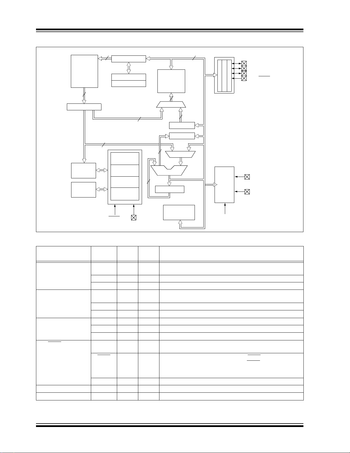
A simplified block diagram is shown in Figure 3-1 with
the corresponding device pins described in Table 3-1.
and digit borrow out bit, respec-
The PIC10F220/222 devices can directly or indirectly
address its register files and data memory. All Special
Function Registers (SFR), including the PC, are
mapped in the data memory. The PIC10F220/222
devices have a highly orthogonal (symmetrical) instruction set that makes it possible to carry out any operation, on any register, using any addressing mode. This
symmetrical nature and lack of “special optimal situations” make programming with the PIC10F220/222
devices simple, yet efficient. In addition, the learning
curve is reduced significantly.
© 2007 Microchip Technology Inc. DS41270E-page 9
PIC10F220/222
Flash
Program
Memory
9-10
Data Bus
8
12
Program
Bus
Instruction Reg
Program Counter
RAM
File
Registers
Direct Addr
5
RAM Addr
9
Addr MUX
Indirect
Addr
FSR Reg
STATUS Reg
MUX
ALU
W Reg
Device Reset
Power-on
Reset
Watchdog
Timer
Instruction
Decode &
Control
Timing
Generation
MCLR
VDD, VSS
Timer0
GPIO
8
8
GP3/MCLR/VPP
GP2/T0CKI/FOSC4
GP1/AN1/ICSPCLK
GP0/AN0/ICSPDAT
5-7
3
STACK1
STACK2
23 or 16
Internal RC
Clock
512 x 12 or
bytes
Timer
256 x 12
ADC
AN1
AN0
Absolute
Voltage
Reference
FIGURE 3-1: BLOCK DIAGRAM
TABLE 3-1: PINOUT DESCRIPTION
Name Function
GP0/AN0/ICSPDAT GP0 TTL CMOS Bidirectional I/O pin. Can be software programmed for internal weak
GP1/AN1/ICSPCLK GP1 TTL CMOS Bidirectional I/O pin. Can be software programmed for internal weak
GP2/T0CKI/FOSC4 GP2 TTL CMOS Bidirectional I/O pin
GP3/MCLR
DD VDD P — Positive supply for logic and I/O pins
V
V
SS VSS P — Ground reference for logic and I/O pins
Legend: I = Input, O = Output, I/O = Input/Output, P = Power, — = Not used, TTL = TTL input,
/VPP GP3 TTL — Input pin. Can be software programmed for internal weak pull-up and
ST = Schmitt Trigger input, AN = Analog Input
AN0 AN — Analog Input
ICSPDAT ST CMOS In-Circuit programming data
AN1 AN — Analog Input
ICSPCLK ST — In-Circuit programming clock
T0CKI ST — Clock input to TMR0
FOSC4 — CMOS Oscillator/4 output
MCLR
V
Input
Type
Output
Type
pull-up and wake-up from Sleep on pin change.
ST — Master Clear (Reset). When configured as M CLR, this pin is an
pull-up and wake-up from Sleep on pin change.
wake-up from Sleep on pin change.
active-low Reset to the device. Voltage on MCLR
PP HV — Programming voltage input
exceed V
Programming mode.
DD during normal device operation or the device will enter
Description
/VPP must not
DS41270E-page 10 © 2007 Microchip Technology Inc.
PIC10F220/222
Q1
Q2 Q3 Q4
Q1
Q2 Q3 Q4
Q1
Q2 Q3 Q4
OSC1
Q1
Q2
Q3
Q4
PC
PC PC + 1 PC + 2
Fetch INST (PC)
Execute INST (PC - 1)
Fetch INST (PC + 1)
Execute INST (PC)
Fetch INST (PC + 2)
Execute INST (PC + 1)
Internal
phase
clock
All instructions are si ngle cycle, exc ept for any program bra nches. These t ake two cycles, since th e fetch instructio n
is “flushed” from the pipeline, while the new instruction is being fetched and then executed.
1. MOVLW 03H
Fetch 1 Execute 1
2. MOVWF GPIO
Fetch 2 Execute 2
3. CALL SUB_1
Fetch 3 Execute 3
4. BSF GPIO, BIT1
Fetch 4 Flush
Fetch SUB_1 Execute SUB_1
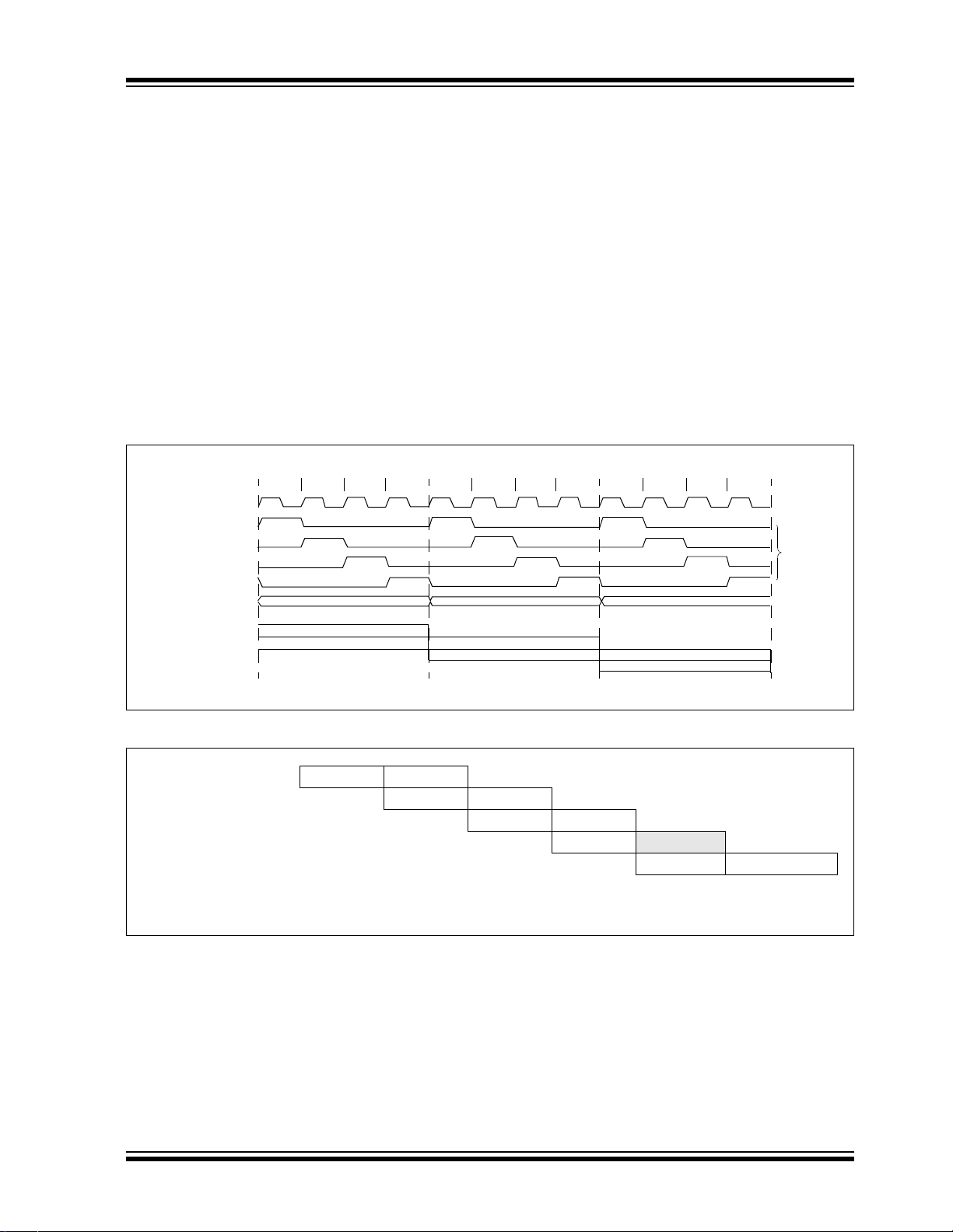
3.1 Clocking Scheme/Instruction Cycle
The clock is internally divided by four to generate four
non-overlapping quadrature clocks, namely Q1, Q2,
Q3 and Q4. Internally, the PC is incremented every Q1,
and the instruction is fetched from program memory
and latched into the Instru ction Regis ter (IR) in Q4. It is
decoded and executed during Q1 through Q4. The
clocks and instruction execution flow is shown in
Figure 3-2 and Example 3-1.
FIGURE 3-2: CLOCK/INSTRUCTION CYCLE
3.2 Instruction Flow/Pipelining
An instruction cycle consists of four Q cycles (Q1, Q2,
Q3 and Q4). The instruction fetch and execute are
pipelined such that fetch takes one instruction cycle,
while decode and execute takes another instruction
cycle. However, due to the pipelining, each instruction
effectively executes in one cycle. If an instruction
causes the PC to change (e.g., GOTO) then two cycles
are required to complete the ins tructi on (Exampl e 3-1).
A fetch cycle begins with the PC incrementing in Q1.
In the execution cy cle, the fetch ed instruction i s latched
into the Instr uction Regist er in cycle Q1. T his instruction is then decoded and executed during the Q2, Q3
and Q4 cycles. Data memory is read during Q2
(operand read) and written during Q4 (destination
write).
EXAMPLE 3-1: INSTRUCTION PIPELINE FLOW
© 2007 Microchip Technology Inc. DS41270E-page 11

PIC10F220/222
NOTES:
DS41270E-page 12 © 2007 Microchip Technology Inc.
PIC10F220/222
CALL, RETLW
PC<7:0>
Stack Level 1
Stack Level 2
User Memory
Space
9
0000h
01FFh
On-chip Program
Memory
Reset Vector
(1)
Note 1: Address 0000h becomes the
effective Reset vector. Location 00FFh
contains the MOVLW XX internal oscillator
calibration value.
256 Word
00FFh
0100h
<8:0>
CALL, RETLW
PC<8:0>
Stack Level 1
Stack Level 2
User Memory
Space
10
0000h
02FFh
Reset Vector
(1)
Note 1: Address 0000h becomes the effective
Reset vector. Location 01FFh contains the
MOVLW XX internal oscillator calibration
value.
512 Words
01FFh
0200h
On-chip Program
Memory
<9:0>
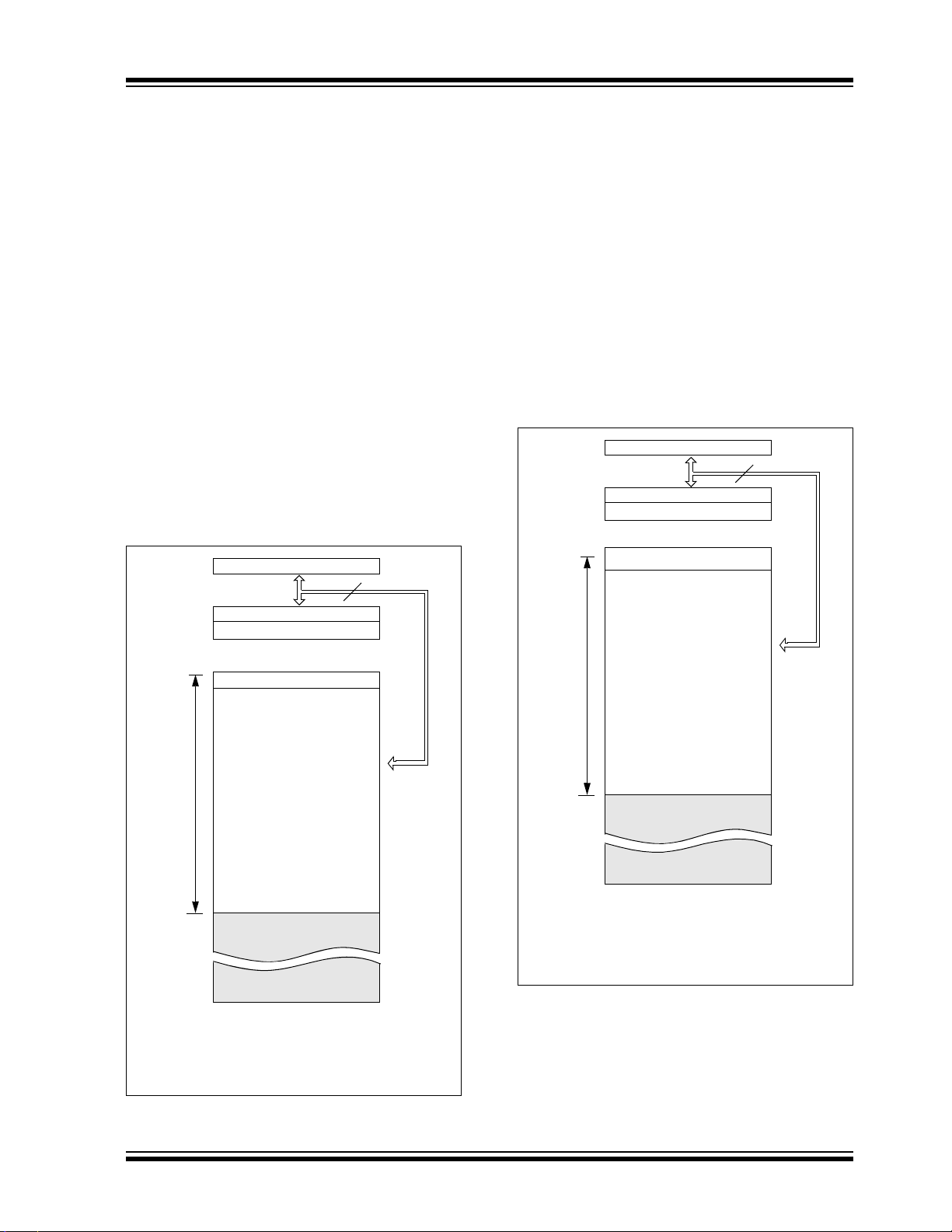
4.0 MEMORY ORGANIZATION
The PIC10F220/222 memories are organized into program memory and data memory. Data memory banks
are accessed using the File Select Register (FSR).
4.1 Program Memory Organization for the PIC10F220
The PIC10F220 devices hav e a 9-bit Prog ram Coun ter
(PC) capable of addressing a 512 x 12 program
memory space.
Only the first 256 x 12 (0000h-00FFh) for the
PIC10F220 are physically implemented (see
Figure 4-1). Accessing a location above these
boundaries will cause a wrap-around within the first
256 x 12 space (PIC10F220). The effective Reset
vector is at 0000h, (see Figure 4-1). Location 00FFh
(PIC10F220) contains the internal clock oscillator
calibration value. This value should never be
overwritten.
FIGURE 4-1: PROGRAM MEMORY MAP
AND STACK FOR THE
PIC10F220
4.2 Program Memory Organization for the PIC10F222
The PIC10F222 devices have a 10-bit Program
Counter (PC) capable of addressing a 1024 x 12
program memory space.
Only the first 512 x 12 (0000h-01FFh) for the MemHigh are physically implemented (see Figure 4-2).
Accessing a location above these boundaries will
cause a wrap-around within the first 512 x 12 space
(PIC10F222). The effective Reset vector is at 0000h,
(see Figure 4-2). Location 01 FFh (PIC10F222) contains the internal clock oscillator calibration value.
This value should never be overwritt en.
FIGURE 4-2: PROGRAM MEMORY MAP
AND STACK FOR THE
PIC10F222
© 2007 Microchip Technology Inc. DS41270E-page 13

PIC10F220/222
File Address
00h
01h
02h
03h
04h
05h
06h
07h
10h
INDF
(1)
TMR0
PCL
STATUS
FSR
OSCCAL
GPIO
General
Purpose
Registers
Note 1: Not a physical register. See Section 4.9
“Indirect Data Addressing; INDF and
FSR Registers”.
2: Unimplemented, read as 00h.
08h
ADCON0
0Fh
1Fh
Unimplemented
(2)
ADRES
09h
File Address
00h
01h
02h
03h
04h
05h
06h
07h
1Fh
INDF
(1)
TMR0
PCL
STATUS
FSR
OSCCAL
GPIO
Note 1: Not a physical register. See Section 4.9
“Indirect Data Addressing; INDF and
FSR Registers”.
08h
ADRES
09h
ADCON0
General
Purpose
Registers
4.3 Data Memory Organization
Data memory is composed of registers or bytes of
RAM. Therefore, d at a memory for a device is specifie d
by its register file. The register file is divided into two
functional groups: Special Function Registers (SFR)
and General Purpose Registers (GPR).
The Special Function Registers include the TMR0 register , the Program Counter (PCL), t he ST A TUS registe r,
the I/O register (GPIO) and the File Select Register
(FSR). In addition, S pecial Function Regi sters are used
to control the I/O port configuration and prescaler
options.
The General Purpose Registers are used for data and
control information under com mand of the instructions .
For the PIC10F220, the register file is composed of 9
Special Function Registers and 16 General Purpose
Registers (Figure 4-3, Figure 4-4).
For the PIC10F222, the register file is composed of 9
Special Function Registers and 23 General Purpose
Registers (Figure 4-4).
4.3.1 GENERAL PURPOSE REGISTER
The General Purpos e Registe r file i s accessed , eithe r
directly o r indirectly, through the F ile Select Regist er
(FSR). See Section 4.9 “Indirect Data Addressing;
INDF and FSR Registers”.
FIGURE 4-3: PIC10F220 REGISTE R
FILE
FILE MAP
FIGURE 4-4: PIC10F222 REGISTER
FILE MAP
4.3.2 SPECIAL FUNCTION REGISTERS
The Special Function Registers (SFRs) are registers
used by the CPU and periph eral functio ns to control the
operation of the device (Table 4-1).
The Special Function Registers can be clas sified into
two sets. Th e Spec ial Function Regist ers associated
with the “core” functions are described in this section.
Those related to the operation of the peripheral
features are described in the section for each
peripheral feature.
DS41270E-page 14 © 2007 Microchip Technology Inc.

PIC10F220/222
TABLE 4-1: SPECIAL FUNCTION REGISTER (SFR) SUMMARY
Address Name Bit 7 Bit 6 Bit 5 Bit 4 Bit 3 Bit 2 Bit 1 Bit 0
00h I NDF Uses contents of FSR to address data memory (not a physical register) xxxx xxxx 20
01h TMR0 8-Bit Real-Time Clock/Counter xxxx xxxx 25
02h PCL
03h STATUS GPWUF
04h FSR Indirect Data Memory Address Pointer 111x xxxx 20
05h OSCCAL CAL6 CAL5 CAL4 CAL3 CAL2 CAL1 CAL0 FOSC4 1111 1110 18
06h GPIO
07h
08h ADRES Result of Analog-to-Digital Conversion xxxx xxxx 31
N/A TRISGPIO
N/A
Legend: – = unimplemented, read as ‘0’, x = unknown, u = unchanged, q = value depends on condition.
Note 1: The upper byte of the Program Counter is not directly accessible. See S ecti on 4.7 “Program Counter” for an
(1)
Low Order 8 Bits of PC 1111 1111 19
— —TOPD ZDCC0--1 1xxx
— — — — GP3 GP2 GP1 GP0 ---- xxxx 21
ADCON0
OPTION
explanation of how to access these bits.
2: Other (non Power-up) Resets include external Reset through MCLR
Reset.
3: See Table8-1 for other Reset specific values.
ANS1 ANS0
— — — — I/O Control Register ---- 1111 23
GPWU
GPPU T0CS T0SE PSA PS2 PS1 PS0 1111 1111 17
— — CHS1 CHS0 GO/DONE ADON 11-- 1100 30
, Watchdog Timer and wake-up on pin change
Value on
Power-On
(2)
Reset
Page #
(3)
15
4.4 STATUS Register
This register contains the arithmetic status of the ALU,
the Reset status and the page preselect bit.
The STATUS register can be the destination for any
instruction, as with any other register. If the STATUS
register is the destination for an instruction that affects
the Z, DC or C bits, then the write to these three bits is
disabled. These bit s are set or cleared ac cording to the
device logic. Furthermore, the TO
writable. Therefore, the result of an instruction with the
STATUS regis ter as destin ation may be diffe rent than
intended.
For example, CLRF STATUS will clear the upper three
bits and set the Z bit. This leaves the STATUS register
as 000u u1uu (where u = unchanged).
Therefore, it is recommended that only BCF, BSF and
MOVWF instructions be used to alter the STATUS register. These instructions do not affect the Z, DC or C bits
from the ST A TUS register . For other ins tructions, whic h
do affect Status bits, see Instruction Set Summary.
and PD bits are not
© 2007 Microchip Technology Inc. DS41270E-page 15

PIC10F220/222
REGISTER 4-1: STATUS REGISTER (ADDRESS: 03h)
R/W-0 R/W-0 R/W-0 R-1 R-1 R/W-x R/W-x R/W-x
GPWUF — —TOPD ZDCC
bit 7 bit 0
Legend:
R = Readable bit W = Writable bit U = Unimplemented bit, read as ‘0’
-n = Value at POR ‘1’ = Bit is set ‘0’ = Bit is cleared x = Bit is unknown
bit 7 GPWUF: GPIO Reset bit
1 = Reset due to wake-up from Sleep on pin change
0 = After power-up or other Reset
bit 6 Reserved: Do not use. Use of this bit may affect upward compatibility with future products.
bit 5 Reserved: Do not use. Use of this bit may affect upward compatibility with future products.
bit 4 TO
bit 3 PD
bit 2 Z: Zero bit
bit 1 DC: Digit carry/borrow
bit 0 C: Carry/borrow bit (for ADDWF, SUBWF and RRF, RLF instructions)
: Time-out bit
1 = After power-up, CLRWDT instruction or SLEEP instruction
0 = A WDT time-out occurred
: Power-down bit
1 = After power-up or by the CLRWDT instruction
0 = By execution of the SLEEP instruction
1 = The result of an arithmetic or logic operation is zero
0 = The result of an arithmetic or logic operation is not zero
bit (for ADDWF and SUBWF instructions)
ADDWF:
1 = A carry to the 4th low-order bit of the result occurred
0 = A carry to the 4th low-order bit of the result did not occur
SUBWF
1 = A borrow from the 4th low-order bit of the result did not occur
0 = A borrow from the 4th low-order bit of the result occurred
ADDWF: SUBWF: RRF or RLF:
1 = A carry occurred 1 = A borrow did not occur Load bit with LSb or MSb, respectively
0 = A carry did not occur 0 = A borrow occurred
:
DS41270E-page 16 © 2007 Microchip Technology Inc.

PIC10F220/222
000
001
010
011
100
101
110
111
1 : 2
1 : 4
1 : 8
1 : 16
1 : 32
1 : 64
1 : 128
1 : 256
1 : 1
1 : 2
1 : 4
1 : 8
1 : 16
1 : 32
1 : 64
1 : 128
Bit Value Timer0 Rate WDT Rate
4.5 OPTION Register
The OPTION register is a 8-bit wide , write-only register ,
which contains various control bits to configure the
Timer0/WDT prescaler and Timer0.
The OPTION register is not memory mapped and is
therefore only addressable by executing the OPTION
instruction, the conten t s of the W registe r will be transferred to the OPTION register. A Reset sets the
OPTION<7:0> bits.
REGISTER 4-2: OPTION REGISTER
W-1 W-1 W-1 W-1 W-1 W-1 W-1 W-1
GPWU
bit 7 bit 0
Legend:
R = Readable bit W = Writable bit U = Unimplemented bit, read as ‘0’
-n = Value at POR ‘1’ = Bit is set ‘0’ = Bit is cleared x = Bit is unknown
GPPU T0CS T0SE PSA PS2 PS1 PS0
Note: If TRIS bit is set to ‘0’, the wake-up on
change and pull-up functions are disabled
for that pin (i.e., note that TRIS overrides
Option control of GPPU
Note: If the T0CS bit is set to ‘1’, it will override
the TRIS function on the T0CKI pin.
and GPWU).
bit 7 GPWU
bit 6 GPPU
bit 5 T0CS: Timer0 Clock Source Select bit
bit 4 T0SE: Timer0 Source Edge Select bit
bit 3 PSA: Prescaler Assignment bit
bit 2-0 PS<2:0>: Prescaler Rate Select bits
: Enable Wake-up On Pin Change bit (GP0, GP1, GP3)
1 = Disabled
0 = Enabled
: Enable Weak Pull-ups bit (GP0, GP1, GP3)
1 = Disabled
0 = Enabled
1 = Transition on T0CKI pin (overrides TRIS on the T0CKI pin)
0 = Transition on internal instruction cyc le clock, F
1 = Increment on high-to-low transition on the T0CKI pin
0 = Increment on low-to-high transition on the T0CKI pin
1 = Prescaler assigned to the WDT
0 = Prescaler assigned to Timer0
OSC/4
© 2007 Microchip Technology Inc. DS41270E-page 17

PIC10F220/222
4.6 OSCCAL Register
The Oscillator Calibrati on (OSCCAL) register is use d to
calibrate the internal precision 4/8 MHz oscillator. It
contains seven bit s for cal ibra tio n
Note: Erasing the device will also erase the pre-
programmed internal ca libration value for
the internal oscillator. The calibration
value must be read prior to erasing the
part so it can be reprogrammed correctly
later.
After you move in the calibration constant, do not
change the value. See Section 8.2.2 “Internal 4/8 MHz
Oscillator”.
REGISTER 4-3: OSCCAL – OSCILLATOR CALIBRATION REGISTER (ADDRESS: 05h)
R/W-1 R/W-1 R/W-1 R/W-1 R/W-1 R/W-1 R/W-1 R/W-0
CAL6 CAL5 CAL4 CAL3 CAL2 CAL1 CAL0 FOSC4
bit 7 bit 0
.
Legend:
R = Readable bit W = Writable bit U = Unimplemented bit, read as ‘0’
-n = Value at POR ‘1’ = Bit is set ‘0’ = Bit is cleared x = Bit is unknown
bit 7-1 CAL<6:0>: Oscillator Calibration bits
0111111 =Maximum frequency
•
•
•
0000001
0000000 =Center frequency
1111111
•
•
•
1000000 =Minimum frequency
(1)
bit 0 FOSC4: INTOSC/4 Output Enable bit
1 = INTOSC/4 output onto GP2
0 = GP2/T0CKI applied to GP2
Note 1: Overrides GP2/T0CKI control registers when enabled.
DS41270E-page 18 © 2007 Microchip Technology Inc.

PIC10F220/222
PC
87 0
PCL
Instruction Word
GOTO Instruction
CALL or Modify PCL Instruction
PC
87 0
PCL
Instruction Word
Reset to ‘0’
4.7 Program Counter
As a program instruction is executed, the Program
Counter (PC) will contain the address of the next
program instruction to be executed. The PC value is
increased by one every instruction cycle, unless an
instruction changes the PC.
For a GOTO instruction, bits 8:0 of the PC are provided
by the GOTO inst ruction word . The PC Latch (P CL) is
mapped to PC<7:0>.
For a CALL instruction or any instruction where the PCL
is the destination, bi t s 7:0 o f the PC ag ain are p rovide d
by the instruction word. However, PC<8> does not
come from the i nstructi on word, but is always c leared
(Figure 4-5).
Instructions where t he PCL is the des tinati on or Modif y
PCL instructi ons, incl ude MOVWF PC, ADDWF PC and
BSF PC, 5.
Note: Because PC<8> is cleared in the CALL
instruction or any Modify PCL instruction,
all subroutine calls or computed jumps are
limited to the first 256 locations of any
program me mory page (512 words l ong).
FIGURE 4-5: LOADING OF PC
BRANCH INSTRUCTIONS
4.7.1 EFFECTS OF RESET
The PC is set upon a Reset, which means that the PC
addresses the last location in program memory (i.e.,
the oscillator calibration instruction). After executing
MOVLW XX, the PC will roll over to location 0000h and
begin executing user code.
4.8 Stack
The PIC10F220 device has a 2-deep, 8-bit wide
hardware PUSH/POP stack.
The PIC10F222 device has a 2-deep, 9-bit wide
hardware PUSH/POP stack.
A CALL instructi on will PU SH the curre nt valu e of stac k
1 into stack 2 and then PUSH the current PC value,
incremented by one, into st ack le vel 1. If more th an two
sequential CALL’s are executed, only the most recent
two return addresses are stored.
A RETLW i nstruction will POP the content s of stack le vel
1 into the PC and then copy stack level 2 contents into
level 1. If more th an two sequen tial RETLW’s are executed, the stack will be filled with the address
previously stored in level 2.
Note 1: The W register will be loaded with the lit-
eral value spec ified in the ins truction. This
is particul arly useful for the im plementation of data look-up tables within the
program memory.
2: There are no Status bits to indicate stack
overflows or stack underflow conditions.
3: There are no instructions mnemonics
called PUSH or POP. These are actions
that occur from the e xecution of the CALL
and RETLW instructions.
© 2007 Microchip Technology Inc. DS41270E-page 19

PIC10F220/222
MOVLW 0x10 ;initialize pointer
MOVWF FSR ;to RAM
NEXT CLRF INDF ;cl e a r I N D F
;register
INCF FSR,F ;inc pointer
BTFSC FSR,4 ;all done?
GOTO NEXT ;NO, clear next
CONTINUE
: ;YES, continue
:
Note 1: For register map detail, see Section 4.3 “D ata Memory Organization”.
Location Select
Location Select
Indirect Addressing
Direct Addressing
Data
Memory
(1)
0Fh
10h
Bank 0
0
4
(FSR)
00h
1Fh
(opcode) 04
4.9 Indirect Data Addressing; INDF and FSR Registers
The INDF register is not a physi cal register. Addressing
INDF actually address es the reg ister whos e addres s is
contained in the FSR regis ter (FSR is a pointer). This is
indirect addressing.
4.9.1 INDIRECT ADDRESSING
• Register file 09 contains the value 10h
• Register file 0A contains the value 0Ah
• Load the value 09 into the FSR register
• A read of the INDF register will return the value
of 10h
• Increment the value of the FSR register by one
(FSR = 0A)
• A read of the INDR register now will return the
value of 0Ah.
Reading INDF itself indirectly (FSR = 0) will produce
00h. Writing to the INDF register indirectly results in a
no-operation (although Status bits may be affected).
A simple program to clear RAM locations 10h-1Fh
using Indirect addressing is shown in Example 4-1.
FIGURE 4-6: DIRECT/INDIRECT ADDRESSING
EXAMPLE 4-1: HOW TO CLEAR RAM
USING INDIRECT
ADDRESSING
The FSR is a 5-bit wide register. It is used in conjunction with the INDF regis ter to indirectly a ddress the dat a
memory area.
The FSR<4:0> bits are used to select data memory
addresses 00h to 1Fh.
Note: Do not use banking. FSR <7:5> are
unimplemented and read as ‘1’s.
DS41270E-page 20 © 2007 Microchip Technology Inc.

PIC10F220/222
Data
Bus
Q
D
Q
CK
Q
D
Q
CK
P
N
WR
Port
TRIS ‘f’
Data
TRIS
RD Port
V
SS
VDD
I/O
pin
W
Reg
Latch
Latch
Reset
Note 1: I/O pins have protection diodes to V
DD and
V
SS.
2: See Table 3-1 for buffer type.
VSS
VDD
(2)
(1)
5.0 I/O PORT
As with any other register, the I/O register(s) can be
written and read under pro gram contro l. However, read
instructions (e.g., MOVF GPIO, W) always read the I/O
pins independent of the pin’s Input/Output modes. On
Reset, all I/O ports are defined as input (inputs are at
high-impedance) sinc e the I/O control registers are all
set.
5.1 GPIO
GPIO is an 8-bit I/O register. Only the low-order 4 bits
are used (GP<3:0>). Bits 7 through 4 are unimplemented and read as ‘0’s. Please note that GP3 is an
input only pin. Pins GP0, GP1 and GP3 can be configured with weak pull-ups and also for wake-up on
change. The wake-up on change and weak pull-up
functions are not individually pin selectable. If GP3/
is configured as MCLR, a weak pull-u p can be
MCLR
enabled via the Configuration Word. Configuring GP3
as MCLR
this pin.
5.2 TRIS Registers
The Output Driver Control register is loaded with the
contents of the W register by executing the TRIS f
instruction. A ‘1’ from a TRIS register bi t puts the corresponding output driver in a High-Impedance mode. A
‘0’ puts the contents of the output data latch on the
selected pins, enabling the output buffer. The exceptions are GP3, whic h is inpu t o nly, and the GP2/T0CKI/
FOSC4 pin, which may be controlled by various
registers. See Table 5 -1.
disables the wake-up on change function for
Note: A read of the ports reads the pins, not the
output data la tches. That is, if an outpu t
driver on a pin is enab led and driv en high,
but the external system is holding it low, a
read of the port will indicate that the pin is
low.
The TRIS registers are “write-only” and are set (output
drivers disabled) upon Re se t.
5.3 I/O Interfacing
The equivalent circuit for an I/O port pin is shown in
Figure 5-1. All port pins, except GP3, which is input
only , ma y be used for both in put and out put operati ons.
For input operations , the se ports are non-latching. Any
input must be present until read by an input instruction
(e.g., MOVF GPIO, W). The outputs are latched and
remain unchanged unt il t he outp ut latc h is rewri tten. To
use a port pin as output, the corresponding direction
control bit in TRIS must be clea red (= 0). For use as an
input, the corresponding TRIS bit must be set. Any I/O
pin (except GP3) can be programmed individually as
input or output.
FIGURE 5-1: EQUIVALENT CIRCUIT
FOR A SINGLE I/O PIN
TABLE 5-1: ORDER OF PRECEDENCE FOR PIN FUNCTIONS
Priority GP0 GP1 GP2 GP3
TABLE 5-2: REQUIREMENTS TO MAKE PINS AVAILABLE IN DIGITAL MODE
FOSC4
T0CS
ANS1
ANS0 0
MCLRE
Legend: — = Condition of bit will have no effect on the setting of the pin to Digital mode.
© 2007 Microchip Technology Inc. DS41270E-page 21
1 AN0 AN1 FOSC4 M
2 TRIS GPIO TRIS GPIO T0CKI —
3
Bit GP0 GP1 GP2 GP3
— — TRIS GPIO —
— — 0 —
— — 0 —
— 0 — —
— — —
— — — 0
CLR

PIC10F220/222
Data
Bus
QD
Q
CK
QD
Q
CK
WR
Port
TRIS ‘f’
Data
TRIS
RD Port
W
Reg
Latch
Latch
Reset
Note 1: I/O pins have protection diodes to VDD and
V
SS.
D
CK
Q
Mis-Match
GPPU
ADC
I/O Pin
(1)
Analog Enable
Data
Bus
QD
Q
CK
QD
Q
CK
WR
Port
TRIS ‘f’
Data
TRIS
RD Port
W
Reg
Latch
Latch
Reset
Note 1: I/O pins have protection diodes to VDD and
V
SS.
T0CKI
I/O Pin
(1)
T0CS
FOSC4
OSCCAL<0>
Data Bus
RD Port
Note 1: GP3/MCLR pin has a protection diode to VSS
only.
GPPU
D
CK
Q
Mis-match
MCLRE
Reset
I/O Pin
(1)
FIGURE 5-2: BLOCK DIAGRAM OF GP0
AND GP1
FIGURE 5-3: BLOCK DIAGRAM OF GP2
FIGURE 5-4: BLOCK DIAGRAM OF GP3
DS41270E-page 22 © 2007 Microchip Technology Inc.

PIC10F220/222
;Initial GPIO Settings
;GPIO<3:2> Inputs
;GPIO<1:0> Outputs
;
; GPIO latch GPIO pins
; ---------- ----------
BCF GPIO, 1 ;---- pp01 ---- pp11
BCF GPIO, 0 ;---- pp10 ---- pp11
MOVLW 007h;
TRIS GPIO ;---- pp10 ---- pp11
;
Note: The user may have expected the pin values to
be ---- pp00. The second BCF caused GP1
to be latched as the pin value (High).
PC PC + 1 PC + 2
PC + 3
Q1 Q2 Q3 Q4 Q1 Q2 Q3 Q4 Q1 Q2 Q3 Q4 Q1 Q2 Q3 Q4
Instruction
Fetched
GP<2:0>
MOVWF GPIO
NOP
Port pin
sampled here
NOP
MOVF GPIO, W
Instruction
Executed
MOVWF GPIO
(Write to GPIO)
NOPMOVF GPIO,W
This example shows a write to GPIO followed
by a read from GPIO.
Data setup tim e = ( 0 .2 5 T
CY – TPD)
where: T
CY = instruction cycle
T
PD = propagation delay
Therefore, at higher clock frequencies, a
write followed by a read may be problematic.
(Read GPIO)
Port pin
written here
T ABLE 5-3: SUMMARY OF PORT REGISTERS
Address Name Bit 7 Bit 6 Bit 5 Bit 4 Bit 3 Bit 2 Bit 1 Bit 0
Value on
Power-On
Reset
Value on
All Other Resets
N/A TRISGPIO
N/A OPTION GPWU
03h STATUS GPWUF
06h GPIO — — — — GP3 GP2 GP1 GP0 ---- xxxx ---- uuuu
Legend: Shaded cells not used by PORT registers, read as ‘0’, – = unimplemented, read as ‘0’, x = unknown, u = unchanged,
q = depends on condition.
Note 1: If Reset was due to wake-up on pin change, then bit 7 = 1. All other Resets will cause bit 7 = 0.
5.4 I/O Programming Considerations
— — — — I/O Control Registers ---- 1111 ---- 1111
GPPU T0CS T0SE PSA PS2 PS1 PS0 1111 1111 1111 1111
— — TO PD Z DC C 0001 1xxx q00q quuu
EXAMPLE 5-1: I/O PORT READ-MODIFY-
WRITE INSTRUCTIONS
5.4.1 BIDIRECTIONAL I/O PORTS
Some instructions operate internally as read followed
by write operations. The BCF and BSF instructions, for
example, read the entire po rt into the CPU, execute the
bit operation and re-write the result. Caution must be
used when these instructions are applied to a port
where one or more pins are used as input/outputs. For
example, a BSF operation on bit 2 of GPIO will cause
all eight bits of GPIO to be read into the CPU, bit 2 to
be set and the GPIO value to be written to the output
latches. If another bit of GPIO is used as a bidire ctional
I/O pin (say bit 0) and it is defined as an input at this
time, the input signal present on the pin itself would be
read into the CPU a nd rewr itten to the d ata latch of thi s
particular pin, overwr iting the previous cont ent. As long
as the pin stays in the Input mode, no problem occurs.
However, if bit 0 is switched into Output mode later on,
the content of the data latch may now be unknown.
Example 5-1 shows the effect of two sequential
Read-Modify-Write instructions (e.g., BCF, BSF, etc.)
on an I/O port.
A pin actively outputting a high or a low should not be
driven from external devices at the same time in order
to change the level o n this pin (“wired-or”, “wired-and”).
The resulting high output currents may damage the
chip.
5.4.2 SUCCESSIVE OPERATIONS ON I/O PORTS
The actual write to an I/O port happens at the end of an
instruction cy cle, whe rea s for readin g, th e data must be
valid at the beginning of the instruction cycle (Figure 5-5).
Therefore, care must be exercised if a write followed by
a read operation is carried out on the same I/O port. The
sequence of instructions should allow the pin voltage to
stabilize (load dependent) before the next instruction
causes that f ile to b e read int o th e CPU . Oth erwis e, t he
previous st ate of that pin may be read into the CPU ra ther
than the new state. When in doubt, it is better to separate
these instruct ions with a NOP or another instruction not
accessing this I/O port.
(1)
FIGURE 5-5: SUCCESSIVE I/O OPERATION
© 2007 Microchip Technology Inc. DS41270E-page 23

PIC10F220/222
NOTES:
DS41270E-page 24 © 2007 Microchip Technology Inc.
 Loading...