


PIC10F200/202/204/206
Data Sheet
6-Pin, 8-Bit Flash Microcontrollers
2004 Microchip Technology Inc. Preliminary DS41239A

Note the following details of the code protection feature on Microchip devices:
• Microchip products meet the specification contained in their particular Microchip Data Sheet.
• Microchip believes that its family of products is one of the most secure families of its kind on the market today, when used in the
intended manner and under normal conditions.
• There are dishonest and possibly illegal methods used to breach the code protection feature. All of these methods, to our
knowledge, require using the Microchip products in a manner outside the operating specifications contained in Microchip’s Data
Sheets. Most likely, the person doing so is engaged in theft of intellectual property.
• Microchip is willing to work with the customer who is concerned about the integrity of their code.
• Neither Microchip nor any other semiconductor manufacturer can guarantee the security of their code. Code protection does not
mean that we are guaranteeing the product as “unbreakable.”
Code protection is constantly evolving. We at Microchip are committed to continuously improving the code protection features of our
products. Attempts to break Microchip’s code protection feature may be a violation of the Digit al Millennium Copyright Act. If suc h a c t s
allow unauthorized access to your software or other copyrighted work, you may have a right to sue for relief under that Act.
Information contained in this publication regarding device
applications and the like is intended through suggestion only
and may be superseded by updates. It is your responsibility to
ensure that your application meets with your specifications.
No representation or warranty is given and no liability is
assumed by Microchip Technology Incorporated with respect
to the accuracy or use of such information, or infringement of
patents or other intellectual property rights arising from such
use or otherwise. Use of Microchip’s products as critical
components in life support systems is not authorized except
with express written approval by Microchip. No licenses are
conveyed, implicitly or otherwise, under any intellectual
property rights.
Trademarks
The Microchip name and logo, the Microchip logo, Accuron,
dsPIC, K
EELOQ, microID, MPLAB, PIC, PICmicro, PICSTART,
PRO MATE, PowerSmart, rfPIC, and SmartShunt are
registered trademarks of Microchip Technology Incorporated
in the U.S.A. and other countries.
AmpLab, FilterLab, MXDEV, MXLAB, PICMASTER, SEEVAL,
SmartSensor and The Embedded Control Solutions Company
are registered trademarks of Microchip Technology
Incorporated in the U.S.A.
Analog-for-the-Digital Age, Application Maestro, dsPICDEM,
dsPICDEM.net, dsPICworks, ECAN, ECONOMONITOR,
FanSense, FlexROM, fuzzyLAB, In-Circuit Serial
Programming, ICSP, ICEPIC, Migra table Memory, MPASM,
MPLIB, MPLINK, MPSIM, PICkit, PICDEM, PICDEM.net,
PICLAB, PICtail, PowerCal, PowerInfo, PowerMate,
PowerTool, rfLAB, rfPICD EM, Select Mode, Smart Serial,
SmartTel and Total Endurance are trademarks of Micro chip
Technology Incorporated in the U.S.A. and other countries.
SQTP is a service mark of Microchip Technology Incorporated
in the U.S.A.
All other trademarks mentioned herein are property of their
respective companies.
© 2004, Microchip Technology Incorporated, Printed in the
U.S.A., All Rights Reserved.
Printed on recycled paper.
Microchip received ISO/TS-16949:2002 quality system certification for
its worldwide headquarters, design and wafer fabrication facilities in
Chandler and Tempe, Arizona and Mountain View, California in
October 2003. The Company’s quality system processes and
procedures are for its PICmicro
devices, Serial EEPROMs, microperipherals, nonvolatile memory and
analog products. In addition, Microchip’s quality system for the design
and manufacture of development systems is ISO 9001:2000 certified.
®
8-bit MCUs, KEELOQ
®
code hopping
DS41239A-page ii Preliminary 2004 Microchip Technology Inc.

PIC10F200/202/204/206
6-Pin, 8-Bit Flash Microcontrollers
Devices Included In This Data Sheet:
•PIC10F200
•PIC10F202
•PIC10F204
•PIC10F206
High-Performance RISC CPU:
• Only 33 single-word instructions to learn
• All single- cycle instructions except for program
branches, which are two-cycle
• 12-bit wide instructions
• 2-level deep hardware stack
• Direct, Indirect and Relative Addressing modes
for data and instructions
• 8-bit wide data path
• 8 Special Function Hardware registers
• Operating speed:
- 4 MHz internal clock
-1µs instruction cycle
Special Microcontroller Features:
• 4 MHz precision internal oscillator:
- Factory calibrated to ±1%
• In-Circuit Serial Programming™ (ICSP™)
• In-Circuit Debugging (ICD) support
• Power-on Reset (PO R)
• Device Reset Tim er (DRT)
• Watchdog Timer (WDT) with dedicated on-chip
RC oscillator for reliable operation
• Programmable code protection
• Multiplexed MCLR
• Internal weak pull-ups on I/O pins
• Power-saving Sleep mode
• Wake-up from Sleep on pin change
input pin
Low-Power Features/CMOS Technology:
• Operating Current:
- < 350 µA @ 2V, 4 MHz
• Standby Current:
- 100 nA @ 2V, typical
• Low-power, high-speed Flash technology:
- 100,000 Flash endurance
- > 40 year retention
• Fully static design
• Wide operating voltage range: 2.0V to 5.5V
• Wide temperature range:
- Industrial: -40°C to +85°C
- Extended: -40°C to +125°C
Peripheral Features (PIC10F200/202):
• 4 I/O pins:
- 3 I/O pins with individual direction control
- 1 input only pin
- High current sink/source for direct LED drive
- Wake-on-change
- Weak pull-ups
• 8-bit real-time cloc k/counter (TMR0) with 8-bit
programmable prescaler
Peripheral Features (PIC10F204/206):
• 4 I/O pins:
- 3 I/O pins with individual direction control
- 1 input only pin
- High current sink/source for direct LED drive
- Wake-on-change
- Weak pull-ups
• 8-bit real-time cloc k/counter (TMR0) with 8-bit
programmable prescaler
• 1 Comparator
- Internal absolute voltage refere nc e
- Both comparator inputs visible externally
- Comparator output visible externally
2004 Microchip Technology Inc. Preliminary DS41239A-page 1
PIC10F200/202/204/206
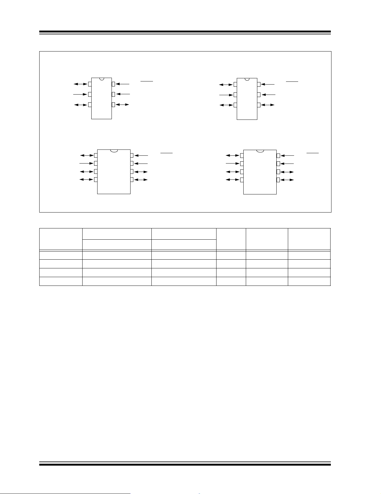
Pin Diagrams
SOT-23
GP0/ICSPDAT
SS
V
GP1/ICSPCLK
PDIP
N/C
VDD
GP2/T0CKI/FOSC4
GP1/ICSPCLK
PIC10F200/202
1
6
2
5
3
4
1
2
3
4
PIC10F200/202
8
7
6
5
GP3/MCLR
VDD
GP2/T0CKI/FOSC4
/VPP
GP3/MCLR/VPP
VSS
N/C
GP0/ICSPDAT
GP0/ICSPDAT/CIN+
GP1/ICSPCLK/CIN-
GP2/T0CKI/COUT/FOSC4
SOT-23
SS
V
PDIP
N/C
VDD
GP1/ICSPCLK/CIN-
PIC10F204/206
1
6
2
5
3
4
1
2
3
4
GP3/MCLR
VDD
GP2/T0CKI/COUT/FOSC4
PIC10F204/206
8
7
6
5
/VPP
GP3/MCLR/VPP
VSS
N/C
GP0/CIN+
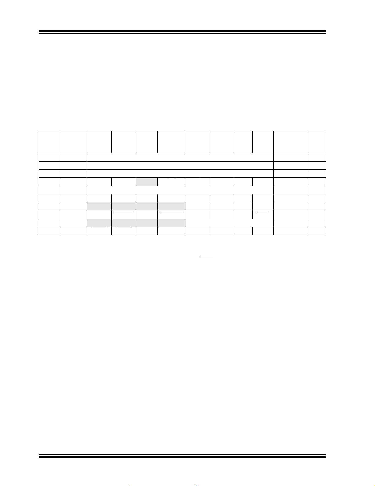
TABLE 1-1: PIC10F2XX MEMORY AND FEATURES
Device
I/O
Flash (words) SRAM (bytes)
PIC10F200 256 16 4 1 0
PIC10F202 512 24 4 1 0
PIC10F204 256 16 4 1 1
PIC10F206 512 24 4 1 1
Program Memory Data Memory
Timers
8-bit
Comparator
DS41239A-page 2 Preliminary 2004 Microchip Technology Inc.

PIC10F200/202/204/206
Table of Contents
1.0 General Description............................................................................ ....... .... .. .... .. .... ................................................................... 5
2.0 PIC10F200/202/204/206 Device Varieties ............... .. .... ..... .... .. .. .... .. .. ....... .. .... .. .. .... ..... .... .. .. .... .. .. ..............................................7
3.0 Architectural Ov erview .................................................................................................................................................................9
4.0 Memory Organization................................................................................................................................................................. 15
5.0 I/O Port.......................................................................................................................................................................................25
6.0 Timer0 Module and TMR0 Register (PIC10F200/202)............................................................................................................... 29
7.0 Timer0 Module and TMR0 Register (PIC10F204/206)............................................................................................................... 33
8.0 Comparator Module................................................................................................... ....... .......................................................... 37
9.0 Special Feature s of th e CPU.......... ....................................................................... .....................................................................41
10.0 Instruction Set Summary............................................................................................................................................................ 51
11.0 Development Support............................................................................................. .................................................................... 59
12.0 Electrical Characteristics............................................................................................................................................................ 65
13.0 DC and AC Characteristics Graphs and Charts......................................................................................................................... 75
14.0 Packaging Information. ............................................................................................................................................................... 77
Index ................................................ . ................................................................................................................................................... 81
On-Line Support................................................................................................................................................................................... 83
Systems Information and Upgrade Hot Line........................................................................................................................................ 83
Reader Response................................................................................................................................................................................ 84
Product Identification System .............................................................................................................................................................. 85
TO OUR VALUED CUSTOMERS
It is our intention to provide our valued customers with t he best docume ntation possible to ensure successf ul use of your Mic rochip products. To this end, we will continue to improve our publications to better suit your needs. Our publications will be refined
and enhanced as new volumes and updates are introduced.
If you have any questions or comments regarding this publication, please contact the Marketing Communications Department via
E-mail at docerrors@mail.microchip.com or fax the Reader Response Form in the back of this data sheet to (480) 792-4150.
We welcome your feedback.
Most Current Data Sheet
To obtain the most up-to-date version of this data sheet, please register at our Worldwide Web site at:
http://www.microchip.com
You can determine the version of a data sheet by examining its literature number found on the bottom outside corner of any page.
The last character of the literature number is the version number, (e.g., DS30000A is version A of document DS30000).
Errata
An errata sheet, describing minor operational differences from the data sheet and recommended workarounds, may exist for current
devices. As device/documentation issues become known to us, we will publish an errata sheet. The errata will specify the revision
of silicon and revision of document to which it applies.
To determine if an errata sheet exists for a particular device, please check with one of the following:
• Microchip’s Worldwide Web site; http://www.microchip.com
• Your local Microchip sales office (see last page)
• The Microchip Corporate Literature Center; U.S. FAX: (480) 792-7277
When contacting a sales office or the literature center, please specify which device, revision of silicon and data sheet (include lit-
erature number) you are using.
Customer Notification System
Register on our web site at www.microchip.com/cn to receive the most current information on all of our products.
2004 Microchip Technology Inc. Preliminary DS41239A-page 3

PIC10F200/202/204/206
NOTES:
DS41239A-page 4 Preliminary 2004 Microchip Technology Inc.
PIC10F200/202/204/206
1.0 GENERAL DESCRIPTION
The PIC10F200/202/204/206 devices from Microchip
T ec hnology are lo w-cost, hig h-performance , 8-bit, fullystatic, Flash-based CMOS microcontrollers. They
employ a RISC architecture with only 33 single-word/
single-cycle instructions. All instructions are single
cycle (1 µs) except for program branches, which take
two cycles. The PIC10F200/202/204/206 devices
deliver performance in an order of magnitude higher
than their competitors in the same price category. The
12-bit wide instructions are highly symmetrical, resulting in a typ ical 2:1 co de compre ssion over o ther 8-bi t
microcontrollers in its class. The easy to use and easy
to remember instruction set reduces development time
significantly.
The PIC10F200/202/204/206 products are equipped
with special features that reduce system cost and
power requirements. The Power-on Reset (POR) and
Device Reset Timer (DRT) eliminate the need for
external Reset circuitry. INTRC Internal Oscillator
mode is provided, thereby preserving the limited
number of I/O available. Power-saving Sleep mode,
Watchdog Timer and code protection features improve
system cost, power and reliabil ity.
The PIC10F200/202/204/206 devices are available in
cost-effective Flash, which is suitable for production in
any volume. The customer can take full advantage of
Microchip’s price leadership in Flash programmable
microcontrollers, while benefiting from the Flash
programmable flexibility.
The PIC10F200/202/204/206 products are supported
by a full-featured macro assembler, a software simulator, an in-circuit debugger, a ‘C’ compiler, a low-cost
development programmer and a full featured programmer. All the tools are supported on IBM
compatible machines.
®
PC and
1.1 Applications
The PIC10F200/202/204/20 6 devices fit in applicati ons
ranging from personal care appliances and security
systems to low-power remote transmitters/receivers.
The Flash technology makes customizing application
programs (transmitter codes, appliance settings,
receiver frequencies, etc.) extremely fast and convenient. The small footpri nt p ackag es, for t hrough h ole or
surface mounting, make these microcontrollers well
suited for application s with sp ac e limit atio ns. Low cos t,
low power, high performance, ease of use and I/O
flexibility make the PIC10F200/202/204/206 devices
very versatile even in areas where no microcontroller
use has been considered before (e.g., timer functions,
logic and PLDs in larger systems and coprocessor
applications).
T ABLE 1-1: PIC10F200/202/204/206 DEVICES
PIC10F200 PIC10F202 PIC10F204 PIC10F206
Clock Maximum Frequency of Operation (MHz) 4 4 4 4
Memory Flash Program Memory 256 512 256 512
Data Memory (bytes) 16 24 16 24
Peripherals Timer Module(s) TMR0 TMR0 TMR0 TMR0
Wake-up from Sleep on Pin Change Yes Yes Yes Yes
Comparators 0 0 1 1
Features I/O Pins 3 3 3 3
Input Only Pins 1 1 1 1
Internal Pull-ups Yes Yes Yes Yes
In-Circuit Serial Programming Yes Yes Yes Yes
Number of Instructions 33 33 33 33
Packages 6-pin SOT-23
8-pin PDIP
The PIC10F200/202/204/206 devices have Power-on Reset, selectable Watchdog Timer, selectable code-protect, high I/O current
capability and precision internal oscillator.
The PIC10F200/202/204/206 device uses serial programming with data pin GP0 and clock pin GP1.
2004 Microchip Technology Inc. Preliminary DS41239A-page 5
6-pin SOT-23
8-pin PDIP
6-pin SOT-23
8-pin PDIP
6-pin SOT-23
8-pin PDIP

PIC10F200/202/204/206
NOTES:
DS41239A-page 6 Preliminary 2004 Microchip Technology Inc.

PIC10F200/202/204/206
2.0 PIC10F200/202/204/206 DEVICE VARIETIES
A variety of packaging options are available. Depending on application and production requirements, the
proper device option can be selected using the
information in th is section. Wh en placing orde rs, please
use the PIC10F200/202 /204 /20 6 Prod uc t Ide ntif ic atio n
System at the back of this data sheet to specify the
correct part number.
2.1 Quick Turn Programming (QTP)
Devices
Microchip offers a QTP programming service for
factory production orders. This service is made
available for users who choose not to program
medium-to-high quantity units and whose code
patterns have stabilized. The devices are identical to
the Flash devices but with all Flash locations and fuse
options already programmed by the factory. Certain
code and prototype verification procedures do apply
before production shipments are available. Please
contact your loc al Microchi p Technology sales of fice for
more details.
2.2 Serialized Quick Turn
Programming
Microchip offers a unique programming service, where
a few user-defined locations in each device are
programmed with different serial numbers. The serial
numbers may be random, pseudo-random or
sequential.
Serial programming allows each device to have a
unique number, which can serve as an entry code,
password or ID number.
SM
(SQTPSM) Devices
2004 Microchip Technology Inc. Preliminary DS41239A-page 7

PIC10F200/202/204/206
NOTES:
DS41239A-page 8 Preliminary 2004 Microchip Technology Inc.

PIC10F200/202/204/206
3.0 ARCHITECTURAL OVERVIEW
The high performance of the PIC10F200/202/204/206
devices can be attributed to a number of architectural
features commonly found in RISC microprocessors. To
begin with, the PIC10F200/202/204/206 devices use a
Harvard architecture in which program and data are
accessed on separate buses. This improves bandwidth over traditional von Neumann architectures
where program and data are fetched on the same bus.
Separating program and data memory further allows
instructions to be sized differently than the 8-bit wide
data word. Instruction opcodes are 12 bits wide,
making it possible to have all single-word instructions.
A 12-bit wide program memory access bus fetches a
12-bit instruction in a single cycle. A two-stage pipeline
overlaps fetch and execution of instructions.
Consequently, all instructions (33) execute in a single
cycle (1 µs @ 4 MHz) except for program branches.
The table belo w lists p rogram me mory (Flash) and data
memory (RAM) for the PIC10F200/202/204/206
devices.
TABLE 3-1: PIC10F2XX MEMORY
Memory
Device
Program Data
PIC10F200 256 x 12 16 x 8
PIC10F202 512 x 12 24 x 8
PIC10F204 256 x 12 16 x 8
PIC10F206 512 x 12 24 x 8
The PIC10F200/202/204/206 devices contain an 8-bit
ALU and working register. The ALU is a general
purpose arithmetic unit. It performs arithmetic and
Boolean functions be tween dat a in the work ing regist er
and any register file.
The ALU is 8 bits wide and capable of addition, subtraction, shift and logical operations. Unless otherwise
mentioned, arithmetic operations are two’s complement in nature. In two-operand instructions, one operand is typically the W (working) register. The other
operand is either a file register or an immediate
constant. In sing le ope ran d inst ruction s, the operan d is
either the W register or a file register.
The W register is an 8-bit workin g register used for ALU
operations. It is not an addressable register.
Depending on the instruction executed, the ALU may
affect the values of the Carry (C), Digit Carry (DC) and
Zero (Z) bits in the Status register. The C and DC bits
operate as a borrow
tively, in subtraction. See the SUBWF and ADDWF
instructions for examples.
A simplified block diagram is shown in Figure 3-1 and
Figure 3-2, with the corresponding device pins
described in Table 3-2.
and digit borrow out bit, respec-
The PIC10F200/202/204/206 devices can directly or
indirectly address its reg ister file s and dat a mem ory. All
Special Function Registers (SFR), including the PC,
are mapped in the data memory. The PIC10F200/202/
204/206 devices have a highly orthogonal
(symmetrica l) instruct ion set that m akes it possib le to
carry out any operation, on any register, using any
addressing mode. This symmetrical nature and lack of
“special optimal situ ations” make programm ing with the
PIC10F200/202/204/206 devices simple, yet efficient.
In addition, the learning curve is reduced significantly.
2004 Microchip Technology Inc. Preliminary DS41239A-page 9

PIC10F200/202/204/206
FIGURE 3-1: PIC10F200/202 BLOCK DIAGRAM
Program
Bus
Flash
512 x12 or
256 x12
Program
Memory
12
Instruction reg
Instruction
Decode &
Control
Timing
Generation
9-10
Program Counter
Direct Addr
8
Device Reset
Power-on
Watchdog
Internal RC
MCLR
Stack 1
Stack 2
Timer
Reset
Timer
Clock
VDD, VSS
RAM Addr
5
Data Bus
RAM
24 or 16
bytes
File
Registers
(1)
Addr MUX
3
ALU
8
W reg
9
Indirect
5-7
FSR reg
Status re g
MUX
Timer0
Addr
8
GPIO
GP0/ICSPDAT
GP1/ICSPCLK
GP2/T0CKI/FOSC4
GP3/MCLR/VPP
DS41239A-page 10 Preliminary 2004 Microchip Technology Inc.

PIC10F200/202/204/206
FIGURE 3-2: PIC10F204/206 BLOCK DIAGRAM
Program
Bus
Flash
512 x12 or
256 x12
Program
Memory
12
Instruction reg
Instruction
Decode &
Control
Timing
Generation
9-10
Program Counter
Direct Addr
8
Device Reset
Power-on
Watchdog
Internal RC
MCLR
Stack 1
Stack 2
Timer
Reset
Timer
Clock
VDD, VSS
RAM Addr
5
Data Bus
RAM
24 or 16
bytes
File
Registers
(1)
Addr MUX
3
ALU
8
W reg
9
Indirect
5-7
FSR reg
Status re g
MUX
Timer0
Addr
8
GPIO
Comparator
GP0/ICSPDAT
GP1/ICSPCLK
GP2/T0CKI/FOSC4
GP3/MCLR/VPP
CIN+
CINCOUT
2004 Microchip Technology Inc. Preliminary DS41239A-page 11

PIC10F200/202/204/206
TABLE 3-2: PIC10F200/202/204/206 PINOUT DESCRIPTION
Name Function
GP0/ICSPDA T/ CIN+ GP0 TTL CMOS Bidirectional I/O pin. Can be software programmed for i nternal
ICSPDAT ST CMOS In -Circu it Serial Programming
CIN+ AN — Comparator input (PIC10F204/206 only).
GP1/ICSPCLK/CIN- GP1 TTL CMOS Bidirectional I/O pin. Can be software programmed for i nternal
ICSPCLK ST CMOS In-Circuit Serial Programming clock pin.
CIN- AN — Comparator input (PIC10F204/206 only).
GP2/T0CKI/COUT/
FOSC4
GP3/MCLR
DD VDD P — Positive supply for logic and I/O pins.
V
VSS VSS P — Ground reference for logic and I/O pins.
Legend: I = Input, O = Output, I/O = Input/Output, P = Power, — = Not used, TTL = TTL input,
/VPP GP3 TTL — Input pin. Can be software programmed for internal weak
ST = Schmitt Trigger input, AN = Analog input
GP2 TTL CMOS Bidirectional I/O pin.
T0CKI ST — Clock input to TMR0.
COUT — CMOS Comparator output (PIC10F204/206 only).
FOSC4 — CMOS Oscillator/4 output.
MCLR
VPP HV — Programming voltage input.
Input
Type
Output
Type
weak pull-up and wake-up from Sleep on pin change.
weak pull-up and wake-up from Sleep on pin change.
pull-up and wake-up from Sleep on pin change.
ST — Master Clear (Reset). When configured as MCLR, this pin is
an active-low Rese t to the de vice. Voltage on GP3/M
must not exceed V
device will enter Programming mode. Weak pull-up alway s on
if configured as MCLR.
Description
™
data pin.
CLR/VPP
DD during normal device operation or the
DS41239A-page 12 Preliminary 2004 Microchip Technology Inc.

PIC10F200/202/204/206
3.1 Clocking Scheme/Instruction
Cycle
The clock is internally divided by four to generate four
non-overlapping quadrature clocks, namely Q1, Q2,
Q3 and Q4. Internal ly, the PC is incremented ev ery Q1
and the instruction is fetched from program memory
and latched into the instruction register in Q4. It is
decoded and execute d during the followin g Q1 throug h
Q4. The clocks and instruction execution flow is shown
in Figure 3-3 and Example 3-1.
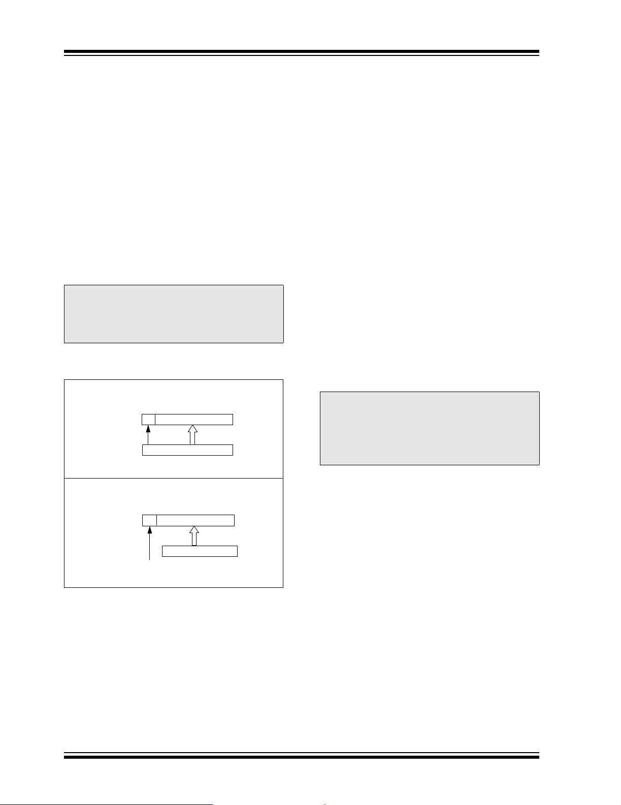
FIGURE 3-3: CLOCK/INSTRUCTION CYCLE
Q2 Q3 Q4
OSC1
Q1
Q2
Q3
Q4
PC
Q1
PC PC+1 PC+2
Q1
3.2 Instruction Flow/Pipelining
An instruction cycle consists of four Q cycles (Q1, Q2,
Q3 and Q4). The instruction fetch and execute are
pipelined such that fetch takes one instruction cycle,
while decode and execute take another instruction
cycle. However, due to the pipelining, each instruction
effectively executes in one cycle. If an instruction
causes the PC to change (e.g ., GOTO), t hen two c yc le s
are required to complete the ins tructi on (Exampl e 3-1).
A fetch cycle begins with the PC incrementing in Q1.
In the execution cy cle, the fetch ed instruction i s latched
into the Instruction Register (IR) in cycle Q1. This
instruction is then decoded and executed during the
Q2, Q3 and Q4 c ycles. Dat a m emory is read during Q2
(operand read) and written during Q4 (destination
write).
Q2 Q3 Q4
Q1
Q2 Q3 Q4
Internal
phase
clock
Fetch INST (PC)
Execute INST (PC – 1)
Fetch INST (PC + 1)
Execute INST (PC)
Fetch INST (PC + 2)
Execute INST (PC + 1)
EXAMPLE 3-1: INSTRUCTION PIPELINE FLOW
1. MOVLW 03H
2. MOVWF GPIO
3. CALL SUB_1
4. BSF GPIO, BIT1
All instructions are si ngle cycle, except for any program bra nches. These tak e two cycles, since th e fetch instruction
is “flushed” from the pipeline, while the new instruction is being fetched and then executed.
Fetch 1 Execute 1
Fetch 2 Execute 2
Fetch 3 Execute 3
Fetch 4 Flush
Fetch SUB_1 Execute SUB_1
2004 Microchip Technology Inc. Preliminary DS41239A-page 13

PIC10F200/202/204/206
NOTES:
DS41239A-page 14 Preliminary 2004 Microchip Technology Inc.
PIC10F200/202/204/206
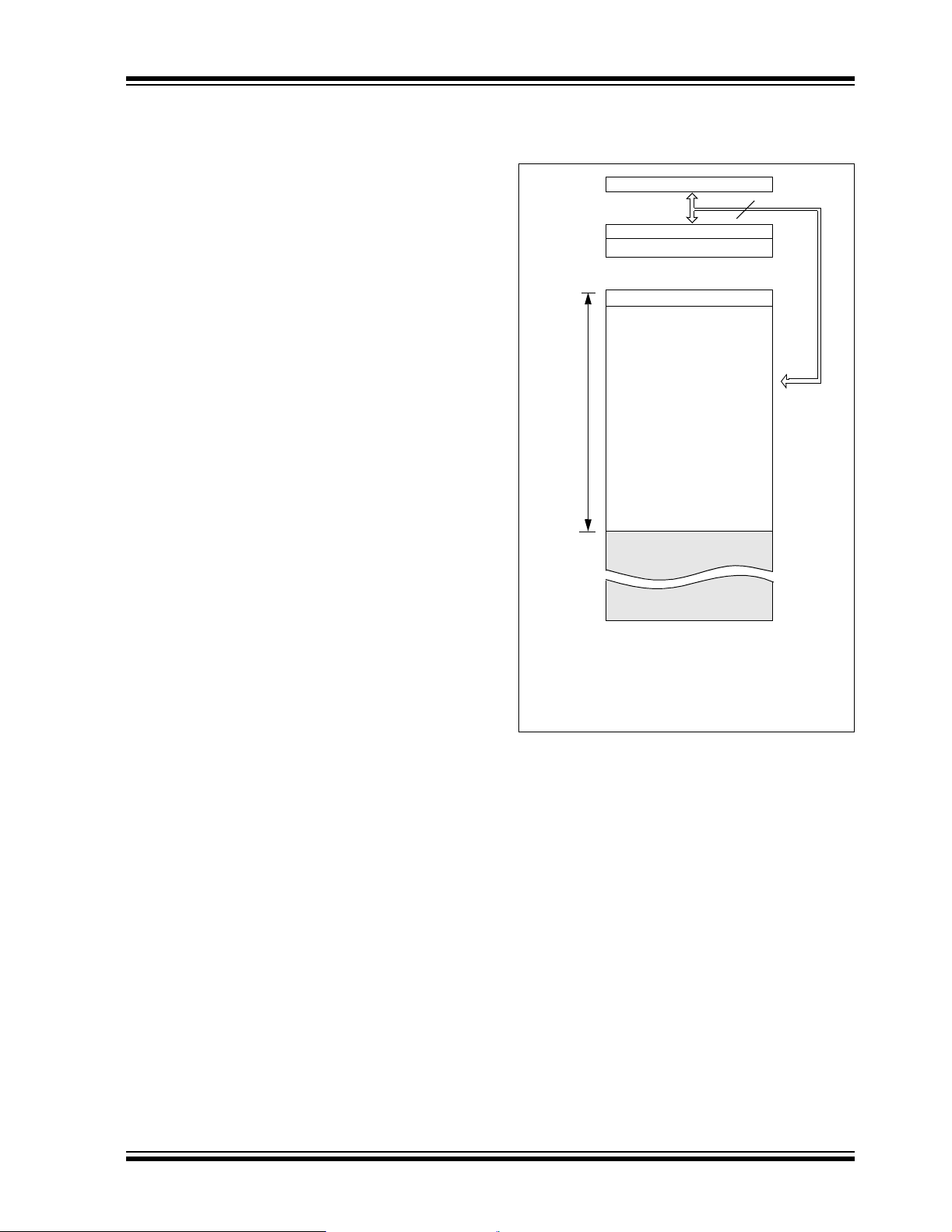
4.0 MEMORY ORGANIZATION
The PIC10F200/202/204/206 memories are organized
into program memory and data memory. Data memory
banks are accessed using the File Select Register
(FSR).
4.1 Program Memory Organization for
the PIC10F200/204
The PIC10F200/204 devices have a 9-bit Program
Counter (PC) capable of addressing a 512 x 12
program memory space.
Only the first 256 x 12 (0000h-00FFh) for the
PIC10F200/204 are physically implemented (see
Figure 4-1). Accessing a location above these
boundaries will cause a wraparound within the first
256 x 12 space (PIC10F200/204). The effective
Reset vector is at 0000h (see Figure 4-1). Location
00FFh (PIC10F200/204) contains the interna l clock
oscillator calibration value. This value should never
be overwritten.
FIGURE 4-1: PROGRAM MEMORY MAP
AND STACK FOR THE
PIC10F200/204
PC<7:0>
CALL, RETLW
Stack Level 1
Stack Level 2
Reset Vector
On-chip Program
Memory
Space
User Memory
256 Word
9
(1)
0000h
00FFh
0100h
Note 1: Address 0000h becomes the
effective Reset vector. Location
00FFh contains the MOVLW XX
internal oscillator calibration value.
01FFh
2004 Microchip Technology Inc. Preliminary DS41239A-page 15
PIC10F200/202/204/206
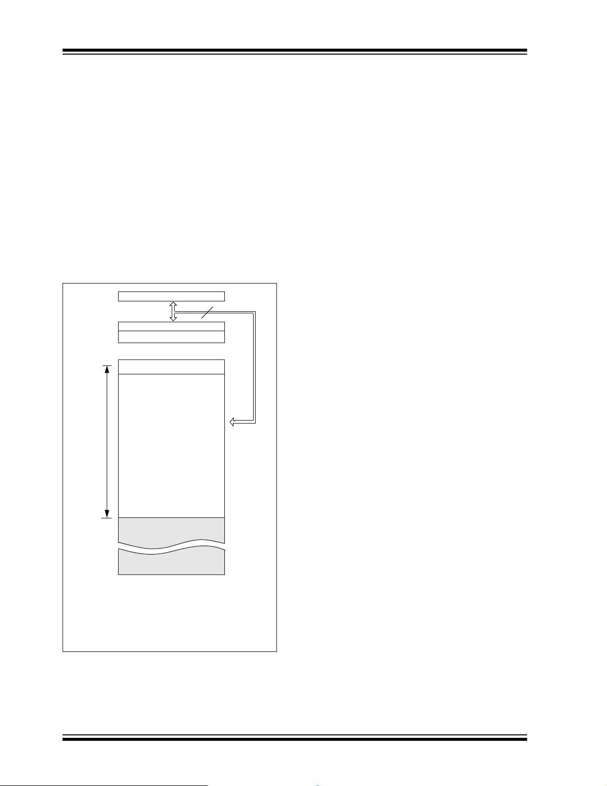
4.2 Program Memory Organization for
the PIC10F202/206
The PIC10F202/206 devices have a 10-bit Program
Counter (PC) capable of addressing a 1024 x 12
program memory space.
Only the first 512 x 12 (0000h-01FFh) for the
PIC10F202/206 are physically implemented (see
Figure 4-2). Accessing a location above these
boundaries will cause a wraparound within the first
512 x 12 space (PIC10F202/206). The effective
Reset vector is at 0000h (see Figure 4-2). Location
01FFh (PIC10F202/206) contains the interna l clock
oscillator calibration value. This value should never
be overwritten.
FIGURE 4-2: PROGRAM MEMORY MAP
AND STACK FOR TH E
PIC10F202/206
PC<8:0>
CALL, RETLW
Stack Level 1
Stack Level 2
Reset Vector
On-chip Program
Memory
10
(1)
0000h
4.3 Data Memory Organization
Data memory is composed of registers or bytes of
RAM. Therefore, da ta memory for a device is sp eci fie d
by its register file. The register file is divided into two
functional groups: Special Function Registers (SFR)
and General Purpose Registers (GPR).
The Special Function Regi st ers in cl ude the TMR0 register, the Program Counter (PCL), the Status register,
the I/O register (GPIO) and the File Select Register
(FSR). In addition, Special Func tion Registers are use d
to control the I/O port configuration and prescaler
options.
The General Purpose Registers are used for data and
control informatio n u nd er com ma nd of the instructions.
For the PIC10F200/204, the register file is composed of
7 Special Function Registers and 16 General Purpose
Registers (see Figure 4-3 and Figure 4-4).
For the PIC10F202/206, the register file is composed of
8 Special Function Registers and 24 General Purpose
Registers (see Figure 4-4).
4.3.1 GENERAL PURPOSE REGISTER
FILE
The General Purpose Register file is accessed, either
directly or indirectly, through the File Select Register
(FSR). See Section 4.9 “Indirect Data Addressing:
INDF and FSR Registers”.
Space
User Memory
512 Words
Note 1: Address 0000h becomes the
effective Reset vector. Location
01FFh contains the MOVLW XX
internal oscillator calibration value.
01FFh
0200h
02FFh
DS41239A-page 16 Preliminary 2004 Microchip Technology Inc.

PIC10F200/202/204/206
FIGURE 4-3: PIC10F200/204 REGISTER
FILE MAP
File Address
(1)
00h
01h
02h
03h
04h
05h
06h
07h
08h
0Fh
10h
1Fh
Note 1: Not a physical register. See Section 4.9
“Indirect Data Addressing: INDF and
FSR Registers”.
2: PIC10F204 only. Unimplemented on the
PIC10F200 and reads as 00h.
3: Unimplemented, read as 00h.
INDF
TMR0
PCL
STATUS
FSR
OSCCAL
GPIO
General
Purpose
Registers
(2)
CMCON0
Unimplemented
(3)
FIGURE 4-4: PIC10F202/206 REGISTER
FILE MAP
File Address
(1)
00h
01h
02h
03h
04h
05h
06h
07h
08h
18h
Note 1: Not a physical register. See Section 4.9
“Indirect Data Addressing: INDF and
FSR Registers”.
2: PIC10F206 only. Unimplemented on the
PIC10F202 and reads as 00h.
INDF
TMR0
PCL
STATUS
FSR
OSCCAL
GPIO
CMCON0
General
Purpose
Registers
(2)
2004 Microchip Technology Inc. Preliminary DS41239A-page 17
PIC10F200/202/204/206
4.3.2 SPECIAL FUNCTION REGISTERS
The Special Function Registers (SFRs) are registers
used by the CPU and per ipheral functio ns to con trol the
operation of the device (Table 4-1).
The Special Function Registers can be classified into
two sets. The Special Function Registers associated
with the “core” functions are described in this section.
Those related to the operation of the peripheral
features are described in the section for each
peripheral feature.
TABLE 4-1: SPECIAL FUNCTION REGISTER (SFR) SUMMARY (PIC10F200/202/204/206)
Address Name Bit 7 Bit 6 Bit 5 Bit 4 Bit 3 Bit 2 Bit 1 Bit 0
00h INDF Uses Contents of FSR to Address Data Memory (not a physical register) xxxx xxxx 23
01h TMR0 8-bit Real-Time Clock/Counter xxxx xxxx 29, 33
(1)
02h
03h STATUS GPWUF CWUF
04h FSR Indirect Data Memory Address Pointer 111x xxxx 23
05h OSCCAL CAL6 CAL5 CAL4 CAL3 CAL2 CAL1 CAL0 FOSC4 1111 1110 21
06h GPIO
07h
N/A TRISGPIO
N/A OPTION GPWU
Legend: — = unimplemented, read as ‘0’, x = unknown, u = unchanged, q = value depends on condition.
Note 1: The upper byte of the Program Counter is not directly accessible. See S ection 4.7 “Program Counter” for an
PCL Low-order 8 bits of PC 1111 1111 22
(5)
—TOPD ZDCC00-1 1xxx
— — — — GP3 GP2 GP1 GP0 ---- xxxx 25
(4)
CMCON0 CMPOUT COUTEN POL CMPT0CS CMPON CNREF CPREF CWU 1111 1111 34
— — — — I/O Control Register ---- 1111 37
GPPU T0CS T0SE PSA PS2 PS1 PS0 1111 1111 20
explanation of how to access these bits.
2: Other (non Power-up) Resets include external Reset through MCLR
Reset.
3: See Table 9-1 for other Reset specific values.
4: PIC10F204/206 only.
5: PIC10F204/206 only. On all other devices, this bit is reserved and should not be used.
, Watchdog Timer and wake-up on pin change
Value on
Power-On
(2)
Reset
(3)
Page #
19
DS41239A-page 18 Preliminary 2004 Microchip Technology Inc.

PIC10F200/202/204/206
4.4 Status Register
This register contains the arithmetic status of the ALU,
the Reset status and the page preselect bit.
The Status register can be the destination for any
instruction, as with any other register. If the Status
register is the destination for an instruction that affects
the Z, DC or C bits, then the write to these three bits is
disabled. These bit s are set or cleared ac cording to the
device logic. Furthermore, the TO
writable. Therefore, the result of an instruction with the
Status register as destination may be different than
intended.
and PD bits are not
For example, CLRF STATUS, will clear the upper three
bits and set the Z bit. Thi s leav es the Status register as
000u u1uu (where u = unchanged).
Therefore, it is recommended that only BCF, BSF and
MOVWF instructions be used to alter the Status register.
These instructions do no t affect the Z, DC or C bit s from
the Status register. For other instructions which do
affect Status bits, see Section 10.0 “Instruction Set
Summary”.
REGISTER 4-1: STATUS REGISTER (ADDRESS: 03h)
R/W-0 R/W-0 R/W-0 R-1 R-1 R/W-x R/W-x R/W-x
GPWUF CWUF
bit 7 bit 0
bit 7 GPWUF: GPIO Reset bit
1 = Reset due to wake-up from Sleep on pin change
0 = After power-up or other Reset
bit 6 CWUF: Comparator Wake-up on Change Flag Bit
1 = Reset due to wake-up from Sleep on comparator change
0 = After power-up or other Reset conditions.
bit 5 Reserved: Do not use. Use of this bit may affect upward compatibility with future products.
bit 4 TO
bit 3 PD
bit 2 Z: Zero bit
bit 1 DC: Digit carry/borrow
bit 0 C: Carry/borrow bit (for ADDWF, SUBWF and RRF, RLF instructions)
: Time-out bit
1 = After power-up, CLRWDT instruction or SLEEP instruction
0 = A WDT time-out occurred
: Power-down bit
1 = After power-up or by the CLRWDT instruction
0 = By execution of the SLEEP instruction
1 = The result of an arithmetic or logic operation is zero
0 = The result of an arithmetic or logic operation is not zero
ADDWF
:
1 = A carry from the 4th low-order bit of the result occurred
0 = A carry from the 4th low-order bit of the result did not occur
:
SUBWF
1 = A borrow from the 4th low-order bit of the result did not occur
0 = A borrow from the 4th low-order bit of the result occurred
ADDWF
: SUBWF: RRF or RLF:
1 = A carry occurred 1 = A borrow did not occur Load bit with LSb or MSb, respectively
0 = A carry did not occur 0 = A borrow occurred
(1)
—TO PD ZDCC
bit (for ADDWF and SUBWF instructions)
(1)
Note 1: This bit is used on the PIC10F204/206. For code compatibili ty do not use this bit on
the PIC10F200/202.
Legend:
R = Readable bit W = Writable bit U = Unimplemented bit, read as ‘0’
-n = Value at POR ‘1’ = Bit is set ‘0’ = Bit is cleared x = Bit is unknown
2004 Microchip Technology Inc. Preliminary DS41239A-page 19

PIC10F200/202/204/206
4.5 Option Register
The Option register is a 8-bit wide, write-only register,
which contains various control bits to configure the
Timer0/WDT prescaler and Timer0.
By executin g the OPTION instruction, the contents of
the W register will be transfe rred to the Option registe r.
A Reset sets the OPTION<7:0> bits.
REGISTER 4-2: OPTION REGISTER
W-1 W-1 W-1 W-1 W-1 W-1 W-1 W-1
GPWU
bit 7 bit 0
GPPU T0CS T0SE PSA PS2 PS1 PS0
Note: If TRIS bit is set to ‘0’, the wake-up on
change and pull-up functions are disabled
for that pin (i.e., note that TRIS overrides
Option control of GPPU
Note: If the T0CS bit is set to ‘1’, it will override
the TRIS function on the T0CKI pin.
and GPWU).
bit 7 GPWU
bit 6 GPPU
bit 5 T0CS: Timer0 Clock Source Select bit
bit 4 T0SE: Timer0 Source Edge Select bit
bit 3 PSA: Prescaler Assignment bit
bit 2-0 PS<2:0>: Prescaler Rate Select bits
: Enable Wake-up on Pin Change bit (GP0, GP1, GP3)
1 = Disabled
0 = Enabled
: Enable Weak Pull-ups bit (GP0, GP1, GP3)
1 = Disabled
0 = Enabled
1 = Transition on T0CKI pin (overrides TRIS on the T0CKI pin)
0 = Transition on internal instruction cycle clock, F
1 = Increment on high-to-low transition on the T0CKI pin
0 = Increment on low-to-high transition on the T0CKI pin
1 = Prescaler assigned to the WDT
0 = Prescaler assigned to Timer0
Bit Value Timer0 Rate WDT Rate
000
001
010
011
100
101
110
111
1 : 2
1 : 4
1 : 8
1 : 16
1 : 32
1 : 64
1 : 128
1 : 256
OSC/4
1 : 1
1 : 2
1 : 4
1 : 8
1 : 16
1 : 32
1 : 64
1 : 128
Legend:
R = Readable bit W = Writable bit U = Unimplemented bit, read as ‘0’
-n = Value at POR ‘1’ = Bit is set ‘0’ = Bit is cleared x = Bit is unknown
DS41239A-page 20 Preliminary 2004 Microchip Technology Inc.

PIC10F200/202/204/206
4.6 OSCCAL Register
The Oscillator Calibrati on (OSCCAL) register is used to
calibrate the internal precision 4 MHz oscillator. It
contains seven bit s for cal ibra tio n
Note: Erasing the device will also erase the pre-
programmed internal calibration value for
the internal oscillator. The calibration
value must be read prior to erasing the
part so it can be reprogrammed correctly
later.
After you move in the calibration constant, do not
change the value. See Section 9.2.2 “Internal 4 MHz
Oscillator”.
REGISTER 4-3: OSCCAL REGISTER (ADDRESS: 05h)
R/W-1 R/W-1 R/W-1 R/W-1 R/W-1 R/W-1 R/W-1 R/W-0
bit 7 bit 0
bit 7-1 CAL<6:0>: Oscillator Calibration bits
0111111 = Maximum frequency
•
•
•
0000001
0000000 = Center frequency
1111111
•
•
•
1000000 = Minimum frequency
bit 0 FOSC4: INTOSC/4 Output Enable bit
1 = INTOSC/4 output onto GP2
0 = GP2/T0CKI/COUT applied to GP2
.
CAL6 CAL5 CAL4 CAL3 CAL2 CAL1 CAL0 FOSC4
(1)
Note 1: Overrides GP2/T0CKI/COUT control registers when enabled.
Legend:
R = Readable bit W = Writable bit U = Unimplemented bit, read as ‘0’
-n = Value at POR ‘1’ = Bit is set ‘0’ = Bit is cleared x = Bit is unknown
2004 Microchip Technology Inc. Preliminary DS41239A-page 21
PIC10F200/202/204/206
4.7 Program Counter
As a program instruction is executed, the Program
Counter (PC) will contain the address of the next
program instruction to be executed. The PC value is
increased by one every instruction cycle, unless an
instruction changes the PC.
For a GOTO instruction, bits 8:0 of the PC are provided
by the GOTO instruction word. The Program Counter
(PCL) is mapped to PC<7:0>.
For a CALL instruction, or any instruction where the
PCL is the destinatio n, bits 7:0 of the PC ag ain are pr ovided by the instruction word. However, PC<8> does
not come from the instruction word, but is always
cleared (Figure 4-5).
Instructions wh ere the PCL is th e destinatio n, or modif y
PCL instructions, include MOVWF PC, ADDWF PC and
BSF PC,5.
Note: Because PC<8> is cleared in the CALL
instruction or any modify PCL instruction,
all subroutine calls or computed jumps are
limited to the first 256 locations of any
program memory page (512 words long).
FIGURE 4-5: LOADING OF PC
BRANCH INSTRUCTIONS
GOTO Instruction
87 0
PC
PCL
Instruction Wor d
4.7.1 EFFECTS OF RESET
The PC is set upon a Reset, which means that the PC
addresses the last location in program memory (i.e.,
the oscillator calibration instruction). After executing
MOVLW XX, the PC will roll over to location 0000h and
begin executing user code.
4.8 Stack
The PIC10F200/204 devi ce s have a 2-deep, 8-b it wid e
hardware PUSH/POP stack.
The PIC10F202/206 devi ce s have a 2-deep, 9-b it wid e
hardware PUSH/POP stack.
A CALL instruction will PUSH the current value of Stack 1
into Stack 2 and then PUSH the current PC value,
incremented by o ne , i nt o Stack Level 1. If m ore th an t w o
sequential CALLs are executed, o nly the mo st recen t two
return addresse s a r e s tor ed .
A RETLW instruction will POP the contents of Stack
Level 1 into the PC and then copy Stack Level 2
contents into level 1. If more than two sequential
RETLWs are execute d, the stack will be fi lled with the
address previously stored in Stack Level 2. Note that
the W register will be loaded with the literal value
specified in the i nstruction. Th is is particu larly useful for
the implementation of data look-up tables within the
program memory.
Note 1: There are no Status bits to indicate stack
overflows or stack underflow conditions.
2: There are no instruction mnemonics
called PUSH or POP. These are actions
that occur from the e xecution of the CALL
and RETLW instructions.
CALL or Modify PCL Instruction
87 0
PC
Reset to ‘0’
DS41239A-page 22 Preliminary 2004 Microchip Technology Inc.
PCL
Instruction Word
PIC10F200/202/204/206
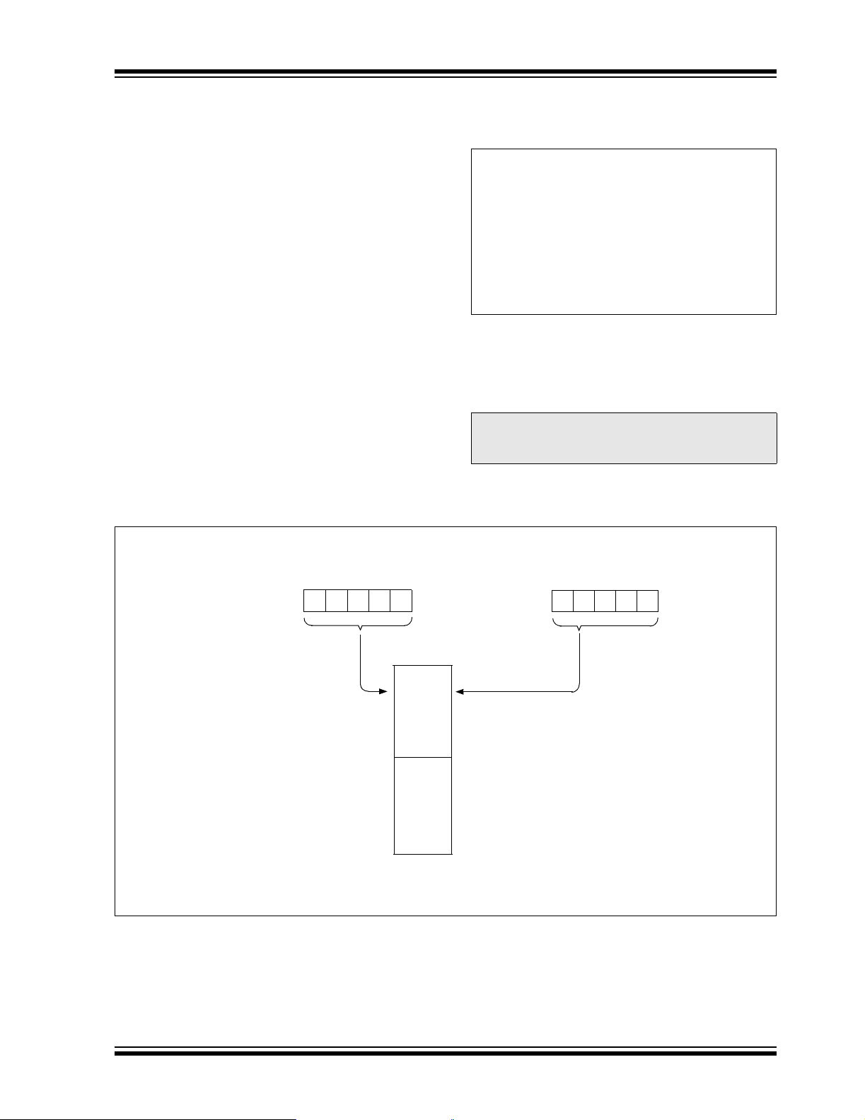
4.9 Indirect Data Addressing: INDF
and FSR Registers
The INDF register is not a physical register.
Addressing INDF actually addresses the register
whose address is contain ed in the FS R reg ist er (FSR
is a pointer). This is indirect addr es sing.
4.10 Indirect Addressing
• Register file 09 contains the value 10h
• Register file 0A contains the value 0Ah
• Load the value 09 into the FSR register
• A read of the INDF register will return the value
of 10h
• Increment the value of the FSR register by one
(FSR = 0A)
• A read of the INDR register now will return the
value of 0Ah.
Reading INDF itself indirectly (FSR = 0) will produce
00h. Writing to the INDF register indirectly results in a
no operation (although Status bits may be affected).
A simple program to clear RAM locations 10h-1Fh
using indirect addressing is shown in Example 4-1.
EXAMPLE 4-1: HOW TO CLEAR RAM
USING INDIRECT
ADDRESSING
MOVLW 0x10 ;initiali ze pointer
MOVWF FSR ;to RAM
NEXT CLRF INDF ;cle a r I N D F
;register
INCF FSR,F ;inc pointer
BTFSC FSR,4 ;all done?
GOTO NEXT ;NO, clear next
CONTINUE
: ;YES, continue
:
The FSR is a 5-bit wide register. It is used in conjunction with the INDF regis ter to indirectly a ddress the dat a
memory area.
The FSR<4:0> bits are used to select data memory
addresses 00h to 1Fh.
Note: PIC10F200/202/204/206 – Do not use
banking. FSR <7:5> are unimplemented
and read as ‘1’s.
FIGURE 4-6: DIRECT/INDIRECT ADDRESSING (PIC10F200/202/204/206)
Direct Addressing
(opcode) 04
Location Select
00h
Data
Memory
Note 1: For register map detail, see Section 4.3 “D ata Memory Organization”.
0Fh
(1)
10h
1Fh
Bank 0
Indirect Addressing
(FSR)
4
Location Select
0
2004 Microchip Technology Inc. Preliminary DS41239A-page 23

PIC10F200/202/204/206
NOTES:
DS41239A-page 24 Preliminary 2004 Microchip Technology Inc.
PIC10F200/202/204/206
5.0 I/O PORT
As with any other register, the I/O register(s) can be
written and read under pro gram contro l. However, read
instructions (e.g., MOVF GPIO, W) always read the I/O
pins independent of the pin’s Input/Output modes. On
Reset, all I/O ports are defined as input (inputs are at
high-impedance) since the I/O control registers are all
set.
5.1 GPIO
GPIO is an 8-bit I/O register. Only the low-order 4 bits
are used (GP<3:0>). Bits 7 through 4 are unimplemented and read as ‘0’s. Please note that GP3 is an
input only pin. Pins GP0, GP1 and GP3 can be configured with weak pull-ups and also for wake-up on
change. The wake-up on change and weak pull-up
functions are not pin s electable. I f GP3/MCLR
ured as MCLR
, weak pull-up is always on and wake-up
on change for this pin is not enabled.
5.2 TRIS Registers
The Output Driver Control register is loaded with the
contents of the W register by executing the TRIS f
instruction. A ‘1’ from a TRIS register bi t puts the corresponding output driver in a High-impedance mode. A
‘0’ puts the contents of the output data latch on the
selected pins, enabling the output buffer. The exceptions are GP3, which is input only and the GP2/T0CKI/
COUT/FOSC4 pin, which may be contro lled by variou s
registers. See Table 5-1.
is config-
5.3 I/O Interfacing
The equivalent circuit for an I/O port pin is shown in
Figure 5-2. All port pins, except GP3 which is input
only , ma y be used for both in put and out put operati ons.
For input operations , the se ports are non-latching. Any
input must be present until read by an input instruction
(e.g., MOVF GPIO, W). The outputs are latched and
remain unchanged unt il t he outp ut latc h is rewri tten. To
use a port pin as output, the corresponding direction
control bit in TRIS must be cleared (= 0). For use as an
input, the corresponding TRIS bit must be set. Any I/O
pin (except GP3) can be programmed individually as
input or output.
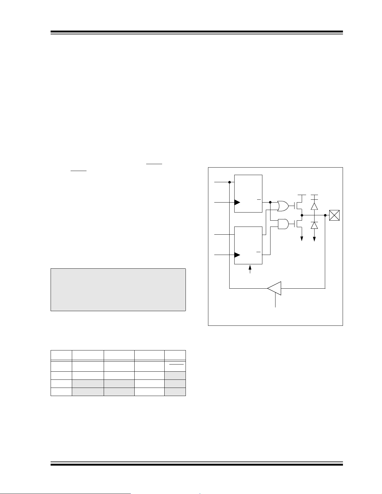
FIGURE 5-1: PIC10F200/202/204/206
EQUIVALENT CIRCUIT
FOR A SINGLE I/O PIN
Data
Bus
WR
Port
W
Reg
TRIS ‘f’
D
D
Data
Latch
CK
TRIS
Latch
CK
Q
VDD
VDD
Q
Q
Q
P
N
SS
VSS
V
I/O
pin
Note: A read of the ports reads the pins, not the
output data latches. That is , if an output
driver on a pin is enab led and driv en high,
but the external system is holding it low, a
read of the port will indicate that the pin is
low.
The TRIS registers are “write-only” and are set (output
drivers disabled) upon Reset.
TABLE 5-1: ORDER OF PRECEDENCE
FOR PIN FUNCTIONS
Priority GP0 GP1 GP2 GP3
1 CIN+ CIN- FOSC4 I/M
2 TRIS GPIO TRIS GPIO COUT —
3
4
— —T0CKI—
— —TRIS GPIO—
CLR
Reset
Note 1: See Table 3-2 for buffer type.
(1)
RD Port
2004 Microchip Technology Inc. Preliminary DS41239A-page 25

PIC10F200/202/204/206
TABLE 5-2: SUMMARY OF PORT REGISTERS
Address Nam e Bit 7 Bit 6 Bit 5 Bit 4 Bit 3 Bit 2 Bit 1 Bit 0
N/A TRISGPIO
N/A OPTION
03h STATUS GPWUF CWUF
06h GPIO — — — — GP3 GP2 GP1 GP0 ---- xxxx ---- uuuu
Legend: Shaded cells are not used by Port registers, read as ‘0’, — = unimplemented, read as ‘0’, x = unknown, u = unchanged,
q = depends on condition.
Note 1: If Reset was due to wake-up on pin change, then bit 7 = 1. All other Resets will cause bit 7 = 0.
2: If Reset was due to wake-up on comparator change, then bit 6 = 1. All other Resets will cause bit 6 = 0.
— —
GPWU
GPPU T0CS T0SE PSA PS2 PS1 PS0 1111 1111 1111 1111
— —
— TO PD Z DC C 00-1 1xxx qq-q quuu
I/O Control Register
Value on
Power-On
Reset
---- 1111 ---- 1111
Value on
All Other Resets
(1, 2)
5.4 I/O Programming Considerations
5.4.1 BIDIREC TION AL I/O PORTS
Some instructions operate internally as read followed
by write operations. The BCF and BSF instructions, for
example, read the entire po rt into the CPU, execute the
bit operation and rewrite the result. Caution must be
used when these instructions are applied to a port
where one or more pins are used as input/ outp uts. For
example, a BSF operation on bit 2 of GPIO will cause
all eight bits of GPIO to be read into the CPU, bit 2 to
be set and the GPIO value to be written to the output
latches. If another bit of GPIO is us ed as a bidire ctional
I/O pin (say bit 0) and it is defined as an input at this
time, the input signal present on the pin itself would be
read into the CPU a nd rewr itten to the d ata latch of thi s
particular pin, overwr iting the previous cont ent. As long
as the pin stays in the Input mode, no problem occurs.
However, if bit 0 is switched into Output mode later on,
the content of the data latch may now be unknown.
Example 5-1 shows the effect of two sequential
Read-Modify-Write instructions (e.g., BCF, BSF, etc.)
on an I/O port.
A pin actively outputting a high or a low should not be
driven from external devices at the same time in order
to change the level on this pin (“wired OR”, “wired
AND”). The resulting high out put current s may damag e
the chip.
EXAMPLE 5-1: READ-MODIFY -WRITE
INSTRUCTIONS ON AN
I/O PORT
;Initial GPIO Settings
;GPIO<3:2> Inputs
;GPIO<1:0> Outputs
;
; GPIO latch GPIO pins
; ---------- ----------
BCF GPIO, 1 ;---- pp01 ---- pp11
BCF GPIO, 0 ;---- pp10 ---- pp11
MOVLW 007h;
TRIS GPIO ;---- pp10 ---- pp11
;
Note 1: The user may have expected the pin values
to be ---- pp00. The 2nd BCF caused GP1
to be latched as the pin value (High).
5.4.2 SUCCESSIVE OPERATIONS ON
I/O PORTS
The actual write to an I/O port happens at the end of an
instruction cy cle, whe rea s for readin g, th e data must be
valid at the beginning of the instruction cycle (Figure 5-2).
Therefore, care must be exercised if a write followed by
a read operation is carried out on the same I/O port. The
sequence of instructions should allow the pin voltage to
stabilize (load dependent) before the next instruction
causes that f ile to b e read int o th e CPU . Oth erwis e, t he
previous stat e of that pin may be re ad into the CPU rathe r
than the new state. When in doubt, it is better to separate
these instru ctions with a NOP or another instruction not
accessing this I/O port.
DS41239A-page 26 Preliminary 2004 Microchip Technology Inc.

PIC10F200/202/204/206
FIGURE 5-2: SUCCESSIVE I/O OPERATION (PIC10F200/202/204/206)
Q1 Q2 Q3 Q4 Q1 Q2 Q3 Q4 Q1 Q2 Q3 Q4 Q1 Q2 Q3 Q4
Instruction
Fetched
GP<2:0>
Instruction
Executed
PC PC + 1 PC + 2
MOVWF GPIO NOP
Port pin
written here
MOVWF GPIO
(Write to GPIO)
Port pin
sampled here
(Read GPIO)
PC + 3
NOPMOVF GPIO, W
NOPMOVF GPIO,W
This example shows a write to GPIO followed
by a read from GPIO.
Data setup time = (0.25 T
where: T
CY = instruction cycle.
PD = propagation delay
T
Therefore, at higher clock frequencies, a
write followed by a read may be problematic.
CY – TPD)
2004 Microchip Technology Inc. Preliminary DS41239A-page 27

PIC10F200/202/204/206
NOTES:
DS41239A-page 28 Preliminary 2004 Microchip Technology Inc.

PIC10F200/202/204/206
6.0 TIMER0 MODULE AND TMR0 REGISTER (PIC10F200/202)
The Timer0 module has the following features:
• 8-bit timer/counter register, TMR0
• Readable and writable
• 8-bit software programmable prescaler
• Internal or external clock select:
- Edge select for external clock
Figure 6-1 is a simplified block diagram of the Timer0
module.
Timer mode is selected by clearing the T0CS bit
(Option<5>). In Timer mode, the Timer0 module will
increment every ins tru cti on cy cl e (w i tho ut p r es ca ler). If
TMR0 register is written, the increment is inhibited for
the following two cycles (Figure 6-2 and Figure 6-3).
The user can work around this by writing an adjusted
value to the TMR0 register.
FIGURE 6-1: TIMER0 BLOCK DIAGRAM
GP2/T0CKI
Pin
T0SE
FOSC/4
0
1
T0CS
Programmable
PS2, PS1, PS0
(1)
Prescaler
Counter mode is selected by setting the T0CS bit
(Option<5>). In this mode, Timer0 will increment either
on every rising or falling edge of pin T0CKI. The T0SE
bit (Option<4>) determines the source edge. Clearing
the T0SE bit selects the ris ing edge. Restrictio ns on the
external clock input are discussed in detail in
Section 6 .1 “Using Timer0 wit h an External Clock
(PIC10F200/202)”.
The prescaler may be used by either the Timer0
module or the Watchdog Timer, but not both. The
prescaler assignment is controlled in software by the
control bit, PSA (Option<3>). Clearing the PSA bit will
assign the prescaler to Timer0. The prescaler is not
readable or writabl e. When the prescaler is assi gned to
the Timer0 module, prescale values of 1:2, 1:4, 1:256
are selectable. Section 6.2 “Prescaler” details the
operation of the prescaler.
A summary of registers associated with the Timer0
module is found in Table6-1.
Data Bus
PS
OUT
1
(2)
3
0
PSA
(1)
(1)
Sync with
Internal
Clocks
(2 TCY delay)
TMR0 reg
PSOUT
Sync
8
Note 1: Bits T0CS, T0SE, PSA, PS2, PS1 and PS0 are located in the Option register.
2: The prescaler is shared with the Watchdog Ti m er (Figure 6-5).
FIGURE 6-2: TIMER0 TIMING: INTERNAL CLOCK/NO PRESCALE
PC
(Program
Counter)
Instruction
Fetch
Timer0
Instruction
Executed
Q1 Q2 Q3 Q4
PC – 1
T0
Q1 Q2 Q3 Q4 Q1 Q2 Q3 Q4 Q1 Q2 Q3 Q4 Q1 Q2 Q3 Q4 Q1 Q2 Q3 Q4 Q1 Q2 Q3 Q4 Q1 Q2 Q3 Q4
PC PC + 1 PC + 2 PC + 3 PC + 4 PC + 6
MOVWF TMR0 MOVF TMR0,W MOVF TMR0,W MOVF TMR0,W MOVF TMR0,W MOVF TMR0,W
T0 + 1 T0 + 2 NT0
Write TMR0
executed
Read TMR0
reads NT0
Read TMR0
reads NT0
Read TMR0
reads NT0
PC + 5
NT0 + 1
Read TMR0
reads NT0 + 1
NT0 + 2
Read TMR0
reads NT0 + 2
2004 Microchip Technology Inc. Preliminary DS41239A-page 29

PIC10F200/202/204/206
FIGURE 6-3: TIMER0 TIMING: INTERNAL CLOCK/PRESCALE 1:2
PC
(Program
Counter)
Instruction
Fetch
Timer0
Instruction
Executed
Q1 Q2 Q3 Q4
PC – 1
T0
Q1 Q2 Q3 Q4 Q1 Q2 Q3 Q4 Q1 Q2 Q3 Q4 Q1 Q2 Q3 Q4 Q1 Q2 Q3 Q4 Q1 Q2 Q3 Q4 Q1 Q2 Q3 Q4
PC PC + 1 PC + 2 PC + 3 PC + 4 PC + 6
MOVWF TMR0 MOVF TMR0,W MOVF TMR0,W MOVF TMR0,W MOVF TMR0,W MOVF TMR0,W
T0 + 1 NT0
Write TMR0
executed
Read TMR0
reads NT0
Read TMR0
reads NT0
Read TMR0
reads NT0
PC + 5
Read TMR0
reads NT0 + 1
TABLE 6-1: REGISTERS ASSOCIATED WITH TIMER0
Address Na m e Bit 7 B it 6 Bit 5 Bit 4 B it 3 Bit 2 Bit 1 Bit 0
01h TMR0 Timer0 – 8-bit Real-Time Clock/Counter xxxx xxxx
N/A OPTION GPWU GPPU T0CS T0SE PSA PS2 PS1 PS0 1111 1111
N/A TRISGPIO
(1)
— —
— —
I/O Control Register ---- 1111
Legend: Shaded cells not used by Timer0. — = unimplemented, x = unknown, u = unchanged.
Note 1: The TRIS of the T0CKI pin is overridden when T0CS = 1.
6.1 Using Timer0 with an External
Clock (PIC10F200/202)
When an external clock input i s used for T i mer0, it must
meet certain requ ir e me nts. The ex t er na l cl oc k req u ir ement is due to internal phas e clock (TOSC) synchroniza-
tion. Also, there is a dela y in the ac tual inc remen ting of
Timer0 after synchronization.
6.1.1 EXTERNAL CLOCK
SYNCHRONIZATION
When no prescaler is used, the external clock input is
the same as the prescaler outp ut. The synch ronization
of T0CKI with the internal phase clocks is accomplished by sampli ng the presc aler output on the Q2 and
Q4 cycles of the internal phase clocks (Figure 6-4).
Therefore, it is necessary for T0CKI to be high for at
least 2 T
for at least 2 T
OSC (and a small RC delay of 2 Tt0H) and low
OSC (and a small RC delay of 2 Tt0H).
Refer to the electrical specification of the desired
device.
When a prescaler is used, the external clock input is
divided by the asynchronous ripple counter-type
prescaler, so that t he presc aler out put is symmetric al.
For the external clock to meet the sampling requirement, the ripple counter must be taken into account.
Therefore, it is necessa ry for T0CKI to h ave a perio d of
at least 4 T
OSC (and a small RC delay of 4 Tt0H) div ided
by the prescaler value. The on ly requirem ent on T0CKI
high and low time is that they do not violate the
minimum pulse width requirement of Tt0H. Refer to
parameters 40 , 41 a nd 42 in the electrical specification
of the desired device.
Value on
Power-On
Reset
NT0 + 1
Read TMR0
reads NT0 + 2
Val ue on
All Other
Resets
uuuu uuuu
1111 1111
---- 1111
DS41239A-page 30 Preliminary 2004 Microchip Technology Inc.

PIC10F200/202/204/206
6.1.2 TIMER0 INCREMENT DELAY
Since the prescaler output is synchronized with the
internal clocks, there is a small delay from the time the
external clock edge occurs to the time the Timer0
module is actually incremented. Figure 6-4 shows the
delay from the external clock edge to the timer
incrementing.
FIGURE 6-4: TIMER0 TIMING WITH EXTERNAL CLOCK
Q1 Q2 Q3 Q4 Q1 Q2 Q3 Q4 Q1 Q2 Q3 Q4 Q1 Q2 Q3 Q4
External Clock Input or
Prescaler Output
External Clock/Prescaler
Output After Sampling
Increment Timer0 (Q4)
(2)
(1)
(3)
Small pulse
misses sampling
Timer0
Note 1: Delay from clock input change to Timer0 increment is 3 T
in measuring the interval between two edges on Timer0 input = ±4 T
2: External clock if no prescaler selected; prescaler output otherwise.
3: The arrows indicate the points in time where sampling occurs.
6.2 Prescaler
An 8-bit counter is available as a prescaler for the
Timer0 module or as a postscaler for the Watchdog
Timer (WDT), respectively (see Section 9.6 “Watch-
dog Timer (WDT)”). For simplicity, this counter is
being referred to as “prescaler” throughout this data
sheet.
Note: The prescaler may be used by either the
Timer0 module or the WDT, but not both.
Thus, a prescaler assignment for the
Timer0 module means that there is no
prescaler for the WDT and vice versa.
The PSA and PS<2:0> bits (Option<3:0>) determine
prescaler assignment and prescale ratio.
When assigned to the Timer0 module, all instructions
writing to the TMR0 register (e.g., CLRF 1, MOVWF 1,
BSF 1,x, etc.) will clear the prescaler . When assi gned
to WDT, a CLRWDT instruction will clear the prescaler
along with the WDT. The prescaler is neither readable
nor writable. On a Reset, the prescal er conta ins all ‘0’s.
T0 T0 + 1 T0 + 2
OSC to 7 T OSC (Duration of Q = TOSC). Therefore, the error
OSC max.
6.2.1 SWITCHING PRESCALER
ASSIGNMENT
The prescaler assignment is fully under software
control (i.e., it can be changed “on-the-fly” during program execution). To avoid an unintended device Re set,
the following instruction sequence (Example 6-1) must
be executed when changing the prescaler assignment
from Timer0 to the WDT.
EXAMPLE 6-1: CHANGIN G PRESCALER
(TIMER0 → WDT)
CLRWDT ;Clear WDT
CLRF TMR0 ;Clear TMR0 & Prescaler
MOVLW ‘00xx1111’b ;These 3 lines (5, 6, 7)
OPTION ;are required only if
;desired
CLRWDT ;PS<2:0> are 000 or 001
MOVLW ‘00xx1xxx’b ;Set Postscaler to
OPTION ;desired WDT rate
2004 Microchip Technology Inc. Preliminary DS41239A-page 31

PIC10F200/202/204/206
To change the prescaler from the WDT to the Timer0
EXAMPLE 6-2: CHANGIN G PRESCALER
module, use the seque nce show n in Example6-2. This
sequence must b e used even if the WDT is dis abled . A
CLRWDT instruction should be executed before
switching the prescaler.
CLRWDT ;Clear WDT and
MOVLW ‘xxxx0xxx’ ;Select TMR0, new
OPTION
FIGURE 6-5: BLOCK DIAGRAM OF THE TIMER0/WDT PRESCALER
TCY (= FOSC/4)
PSA
0
M
U
X
1
(1)
T0CS
M
U
X
(1)
8-bit Prescaler
8-to-1MUX
1
M
U
X
0
(1)
PSA
8
PS<2:0>
GP2/T0CKI
Pin
Watchdog
Timer
(2)
T0SE
(1)
0
1
(WDT→TIMER0)
;prescaler
;prescale value and
;clock source
Data Bus
Sync
2
Cycles
(1)
TMR0 reg
8
WDT Enable bit
Note 1: T0CS, T0SE, PSA, PS<2:0> are bits in the Option register.
2: T0CKI is shared with pin GP2 on the PIC10F200/202/204/206.
0
MUX
WDT
Time-Out
1
(1)
PSA
DS41239A-page 32 Preliminary 2004 Microchip Technology Inc.

PIC10F200/202/204/206
7.0 TIMER0 MODULE AND TMR0 REGISTER (PIC10F204/206)
The Timer0 module has the following features:
• 8-bit timer/counter register, TMR0
• Readable and writable
• 8-bit software programmable prescaler
• Internal or external clock select:
- Edge select for external clock
- External clock from either the T0CKI pin or
from the output of the comparator
Figure 7-1 is a simplified block diagram of the Timer0
module.
Timer mode is selected by clearing the T0CS bit
(Option<5>). In Timer mode, the Timer0 module will
increment every ins tru cti on cy cl e (w i tho ut p r es ca ler). If
TMR0 register is written, the increment is inhibited for
the following two cycles (Figure 7-2 and Figure 7-3).
The user can work around this by writing an adjusted
value to the TMR0 register.
There are two types of Counter mo de. The first Counter
mode uses the T0CKI pin to increment Timer0. It is
selected by setting the T0CS bit (Option<5>), setting
the CMPT0CS
COUTEN
increment either on every rising or falling edge of pin
T0CKI. The T0SE bit (Option<4>) determines the
source edge. Clearing the T0SE bit selects the rising
edge. Restrictions on the external clock input are
discussed in detail in Section 7.1 “Using Timer0 with
an External Clock (PIC10F204 /206)”.
bit (CMCON0<4>) and setting the
bit (CMCON0<6>). In this mode, Timer0 will
The second Counter mo de use s the out put of the comparator to increment Timer0. It can be entered in two
different ways. The first way is selected by setting the
T0CS bit (Option<5>) and clearing the CMPT0CS
(CMCON<4>); (COUTEN
([CMCON<6>]) does not
bit
affect this mode of operation. This enables an internal
connection between the comparator and the Timer0.
The second way is selected by setting the T0CS bit
(Option<5>), setting the CMPT0CS
and clearing the COUTEN
bit (CMCON0<4>)
bit (CMCON0<6>). This
allows the output of t he compa rator onto the T0 CKI pin,
while keeping the T0CKI input active. Therefore, any
comparator change on the COUT pin is fed back into
the T0CKI input. The T0SE bit (Op tion<4> ) determi nes
the source edge. Clearing the T0SE bit selects the
rising edge. Restrictions on the external clock input as
discussed in Section 7.1 “Using Timer0 with an
External Clock (PIC10F204/206)”
The prescaler may be used by either the Timer0
module or the Watchdog Timer, but not both. The
prescaler assignment is controlled in software by the
control bit, PSA (Option<3>). Clearing the PSA bit will
assign the prescaler to Timer0. The prescaler is not
readable or writabl e. When the prescaler is assi gned to
the Timer0 module, prescale values of 1:2, 1:4,...,
1:256 are selectable. Section 7.2 “Prescaler” details
the operation of the prescaler.
A summary of registers associated with the Timer0
module is found in Table7-1.
FIGURE 7-1: TIMER0 BLOCK DIAGRAM (PIC10F204/206)
T0CKI
Pin
FOSC/4
Internal
Comparator
Output
Note 1: Bits T0CS, T0SE, PSA, PS2, PS1 and PS0 are located in the Option register.
2: The prescaler is shared with the Watchdog Timer (Figure 7-5).
3: Bit CMPT0CS
1
0
CMPT0CS
(1)
T0SE
(3)
is located in the CMCON0 register, CMCON0<4>.
0
T0CS
1
(1)
Programmable
Prescaler
3
PS2, PS1, PS0
PS
1
(2)
0
PSA
(1)
(1)
OUT
(2 TCY delay)
Sync with
Internal
Clocks
Data Bus
8
TMR0 reg
PSOUT
Sync
2004 Microchip Technology Inc. Preliminary DS41239A-page 33

PIC10F200/202/204/206
FIGURE 7-2: TIMER0 TIMING: INTERNAL CLOCK/NO PRESCALE
PC
(Program
Counter)
Instruction
Fetch
Timer0
Instruction
Executed
Q1 Q2 Q3 Q4
PC – 1
T0
Q1 Q2 Q3 Q4 Q1 Q2 Q3 Q4 Q1 Q2 Q3 Q4 Q1 Q2 Q3 Q4 Q1 Q2 Q3 Q4 Q1 Q2 Q3 Q4 Q1 Q2 Q3 Q4
PC PC + 1 PC + 2 PC + 3 PC + 4 PC + 6
MOVWF TMR0 MOVF TMR0,W MOVF TMR0,W MOVF TMR0,W MOVF TMR0,W MOVF TMR0,W
T0 + 1 T0 + 2 NT0
Write TMR0
executed
Read TMR0
reads NT0
Read TMR0
reads NT0
Read TMR0
reads NT0
PC+5
NT0 + 1
Read TMR0
reads NT0 + 1
NT0 + 2
Read TMR0
reads NT0 + 2
FIGURE 7-3: TIMER0 TIMING: INTERNAL CLOCK/PRESCALE 1:2
PC
(Program
Counter)
Instruction
Fetch
Timer0
Instruction
Executed
Q1 Q2 Q3 Q4
PC – 1
T0
Q1 Q2 Q3 Q4 Q1 Q2 Q3 Q4 Q1 Q2 Q3 Q4 Q1 Q2 Q3 Q4 Q1 Q2 Q3 Q4 Q1 Q2 Q3 Q4 Q1 Q2 Q3 Q4
PC PC + 1 PC + 2 PC + 3 PC + 4 PC + 6
MOVWF TMR0 MOVF TMR0,W MOVF TMR0,W MOVF TMR0,W MOVF TMR0,W MOVF TMR0,W
T0 + 1 NT0
Write TMR0
executed
Read TMR0
reads NT0
Read TMR0
reads NT0
Read TMR0
reads NT0
PC + 5
Read TMR0
reads NT0 + 1
NT0 + 1
Read TMR0
reads NT0 + 2
TABLE 7-1: REGISTERS ASSOCIATED WITH TIMER0
Address Name Bit 7 Bit 6 Bit 5 Bit 4 Bit 3 Bit 2 Bit 1 Bit 0
01h TMR0 Timer0 – 8-bit Real-Time Clock/Counter xxxx xxxx uuuu uuuu
07h CMCON0
N/A OPTION
N/A TRISGPIO
CMPOUT COUTEN
GPWU GPPU T0CS T0SE PSA PS2 PS1 PS0 1111 1111 1111 1111
(1)
— — — — I/O Control Register ---- 1111 ---- 1111
POL CMPT0CS CMPON CNREF CPREF CWU 1111 1111 uuuu uuuu
Value on
Power-On
Reset
Legend: Shaded cells not used by Timer0. — = unimplemented, x = unknown, u = unchanged.
Note 1: The TRIS of the T0CKI pin is overridden when T0CS = 1.
Value on
All Other
Resets
7.1 Using Timer0 with an External
Clock (PIC10F204/206)
When an external clock input i s used for T i mer0, it must
meet certain requ ir e me nts. The ex t er na l cl oc k req u ir ement is due to internal phas e clock (TOSC) synchroniza-
tion. Also, there is a dela y in the ac tual inc remen ting of
Timer0 after synchronization.
7.1.1 EXTERN AL CLOCK
SYNCHRONIZATION
When no pr escal er is us ed, t he ex ternal clock inpu t is
the same as the prescaler outp ut. Th e synchronization
of an external clock with the internal phase clocks is
accomplished by sampling the prescaler output on the
Q2 and Q4 cycles of the internal phase clocks
small RC delay of 2 Tt0H) and low for at least 2 T
(and a small RC delay of 2 Tt 0H). Refer to the electri cal
specification of the desired device.
When a prescaler is used, the external clock input is
divided by the asynchronous ripple counter type
prescaler, so that t he presc aler out put is symmetric al.
For the external clock to meet the sampling requirement, the ripple counter must be taken into account.
Therefore, it is necessary for T0CKI or the comparator
output to ha ve a p er i od of at le a st 4 T
OSC (and a small
RC delay of 4 Tt0H) divided by the pre scaler value. The
only requirement on T0CKI or the comparator output
high and low time is that they do not violate the
minimum pulse width requirement of Tt0H. Refer to
parameters 40 , 41 a nd 42 in the electrical specification
of the desired device.
OSC
(Figure 7-4). Therefore, it is neces sary for T0CKI or the
comparator out put to b e h igh for a t l eas t 2 T
DS41239A-page 34 Preliminary 2004 Microchip Technology Inc.
OSC (and a

PIC10F200/202/204/206
7.1.2 TIMER0 INCREMENT DELAY
Since the prescaler output is synchronized with the
internal clocks, there is a small delay from the time the
external clock edge occurs to the time the Timer0
module is actually incremented. Figure 7-4 shows the
delay from the external clock edge to the timer
incrementing.
FIGURE 7-4: TIMER0 TIMING WITH EXTERNAL CLOCK
Q1 Q2 Q3 Q4 Q1 Q2 Q3 Q4 Q1 Q2 Q3 Q4 Q1 Q2 Q3 Q4
External Clock Input or
Prescaler Output
External Clock/Prescaler
Output After Sampling
Increment Timer0 (Q4)
(2)
(1)
(3)
Small pulse
misses sampling
Timer0
Note 1: Delay from clock input change to Timer0 increment is 3 T
in measuring the interval between two edges on Timer0 input = ±4 T
2: External clock if no prescaler selected; prescaler output otherwise.
3: The arrows indicate the points in time where sampling occurs.
7.2 Prescaler
An 8-bit counter is available as a prescaler for the
Timer0 module or as a postscaler for the Watchdog
Timer (WDT), respectively (see Figure 9-6). For
simplicity, this counter is being referred to as
“prescaler” throughout this data sheet.
Note: The prescaler may be used by either the
Timer0 module or the WDT, but not both.
Thus, a prescaler assignment for the
Timer0 module means that there is no
prescaler for the WDT and vice versa.
The PSA and PS<2:0> bits (Option<3:0>) determine
prescaler assignment and prescale ratio.
When assigned to the Timer0 module, all instructions
writing to the TMR0 register (e.g., CLRF 1, MOVWF 1,
BSF 1,x, etc.) will clear the prescaler . When assi gned
to WDT, a CLRWDT instruction will clear the prescaler
along with the WDT. The prescaler is neither readable
nor writable. On a Reset, the prescal er conta ins all ‘0’s.
T0 T0 + 1 T0 + 2
OSC to 7 T OSC (Duration of Q = TOSC). Therefore, the error
OSC max.
7.2.1 SWITCHING PRESCALER
ASSIGNMENT
The prescaler assignment is fully under software
control (i.e., it can be changed “on-the-fly” during program execution). To avoid an unintended device Re set,
the following instruction sequence (Example 7-1) must
be executed when changing the prescaler assignment
from Timer0 to the WDT.
EXAMPLE 7-1: CHANGIN G PRESCALER
(TIMER0 → WDT)
CLRWDT ;Clear WDT
CLRF TMR0 ;Clear TMR0 & Prescaler
MOVLW ‘00xx1111’b ;These 3 lines (5, 6, 7)
OPTION ;are required only if
;desired
CLRWDT ;PS<2:0> are 000 or 001
MOVLW ‘00xx1xxx’b ;Set Postscaler to
OPTION ;desired WDT rate
2004 Microchip Technology Inc. Preliminary DS41239A-page 35

PIC10F200/202/204/206
To change the prescaler from the WDT to the Timer0
EXAMPLE 7-2: CHANGIN G PRESCALER
module, use the se quenc e sho wn i n Exampl e 7.2. This
sequence must b e used even if the WDT is dis abled . A
CLRWDT instruction should be executed before
switching the prescaler.
CLRWDT ;Clear WDT and
MOVLW ‘xxxx0xxx’ ;Select TMR0, new
OPTION
FIGURE 7-5: BLOCK DIAGRAM OF THE TIMER0/WDT PRESCALER
Pin
(2)
TCY (= FOSC/4)
1
0
CMPT0CS
Watchdog
Timer
T0SE
(3)
0
M
U
X
1
(1)
0
M
U
X
1
(1)
PSA
T0CS
(1)
8-bit Prescaler
8-to-1MUX
1
M
U
X
0
(1)
PSA
8
PS<2:0>
GP2/T0CKI
Comparator
Output
(WDT→TIMER0)
;prescaler
;prescale value and
;clock source
Data Bus
Sync
2
Cycles
(1)
TMR0 reg
8
WDT Enable bit
Note 1: T0CS, T0SE, PSA, PS<2:0> are bits in the Option register.
2: T0CKI is shared with pin GP2.
3: Bit CMPT0CS
is located in the CMCON0 register.
0
Time-out
MUX
WDT
1
(1)
PSA
DS41239A-page 36 Preliminary 2004 Microchip Technology Inc.

PIC10F200/202/204/206
8.0 COMPARATOR MODULE
The Comparator module contains one analog
comparator. The inputs to the comparator are
multiplexed with GP0 and GP1 pins. The output of the
comparator can be placed on GP2.
The CMCON0 register, shown in Register 8-1, controls
the comparator operation. A block diagram of the
comparator is shown in Figure 8-1.
REGISTER 8-1: CMCON0 REGISTER (ADDRESS: 07h)
R-1 R/W-1 R/W-1 R/W-1 R/W-1 R/W-1 R/W-1 R/W-1
CMPOUT COUTEN
bit 7 bit 0
bit 7 CMPOUT: Comparator Output bit
1 = VIN+ > VIN-
0 = V
IN+ < VIN-
bit 6 COUTEN: Comparator Output Enable bit
1 = Output of comparator is NOT placed on the COUT pin
0 = Output of comparator is placed in the COUT pin
bit 5 POL: Comparator Output Polarity bit
1 = Output of comparator not inverted
0 = Output of comparator inverted
bit 4 CMPT0CS
: Comparator TMR0 Clock Source bit
1 = TMR0 clock source selected by T0CS control bit
0 = Comparator output used as TMR0 clock source
bit 3 CMPON: Comparator Enable bit
1 = Comparator is on
0 = Comparator is off
bit 2 CNREF: Comparator Negative Reference Select bit
1 = CIN- pin
(3)
0 = Internal voltage reference
bit 1 CPREF: Comparator Positive Reference Select bit
1 = CIN+ pin
0 = CIN- pin
(3)
(3)
bit 0 CWU: Comparator Wake-up on Change Enable bit
1 = Wake-up on comparator change is disabled
0 = Wake-up on comparator change is enabled.
POL CMPT0CS CMPON CNREF CPREF CWU
(1, 2)
(2)
(2)
(2)
(2)
(2)
Note 1: Overrides T0CS bit for TRIS control of GP2.
2: When the comparator is turned on, these control bits assert themselves. When the
comparator is off, these bits have no effect on the device operation and the other
control registers have precedence.
3: PIC10F204/206 only.
Legend:
R = Readable bit W = Writable bit U = Unimplemented bit, read as ‘0’
-n = Value at POR ‘1’ = Bit is set ‘0’ = Bit is cleared x = Bit is unknown
2004 Microchip Technology Inc. Preliminary DS41239A-page 37

PIC10F200/202/204/206
8.1 Comparator Configuration
The on-board comparator inputs, (GP0/CIN+, GP1/
CIN-), as well as the comparator output (GP2/COUT)
are steerable. The CMCON0, OPTION, and TRIS
registers are used t o s teer t hes e p ins (s ee Fi gu re 8-1).
If the Comparator mode is changed, the comparator
output level may not be valid for the specified mode
change delay shown in Table 12-1.
Note: The comparator can have an inverted
FIGURE 8-1: BLOCK DIAGRAM OF THE COMPARATOR
CPREF
C+
C-
OSCCAL
Band Gap Buffer
(0.6V)
CNREF
+
-
POL
CMPON
T0CKI
output (see Figure8-1).
T0CKI/GP2/COUT
OUTEN
C
COUT(Register)
T0CKI Pin
CWU
TABLE 8-1: TMR0 CLOCK SOURCE
FUNCTION MUXING
T0CS CMPT0CS COUTEN Source
0x xInternal In stru cti on
Cycle
10 0CMPOUT
10 1CMPOUT
11 0CMPOUT
11 1T0CKI
T0CKSEL
CWUF
QD
S
READ
CMCON
DS41239A-page 38 Preliminary 2004 Microchip Technology Inc.

PIC10F200/202/204/206
8.2 Comparator Operation
A single comparator is shown in Figure 8-2 along with
the relationship between the analog input levels and
the digital output . When the analo g input a t V
than the analog input V
is a digital low level. When the analog input at V
greater than the analog input V
comparator is a digital high level. The shaded areas of
the output of the comparator in Figure 8-2 represent
the uncertainty due to input offsets and response time.
See Table 12-1 for Common Mode Voltage.
IN-, the output of the compara tor
IN-, the output of the
IN+ is less
IN+ is
FIGURE 8-2: SINGLE COMPARATOR
Vin+
Vin-
VIN-
VIN+
Result
+
Result
–
8.3 Comparator Reference
An internal reference signa l may be used depend ing on
the comparator operatin g mode. T he analo g signal th at
is present at V
the digital output of the comparator is adjusted
accordingly (Figure 8-2). Please see Table 12-1 for
internal reference specifications.
IN- is compared to the signal at VIN+ and
8.4 Comparator Response Time
8.5 Comparator Output
The comparator output is read through CMCON0
register. This bit is read-only. The comparator output
may also be used internally, see Figure 8-1.
Note: Analog levels on any pin that is defin ed as
a digital inpu t may cause the input buffer to
consume more current than is specified.
8.6 Comparator Wake-up Flag
The comparator wake-up flag i s set w henev er all o f the
following conditions are met:
•CWU = 0 (CMCON0 <0>)
• CMCON0 has been read to latch the last known
state of the CMPOUT bit (MOVF CMCON0, W)
• Device is in Sleep
• The output of the comparator has changed state
The wake-up flag may be cleared in software or by
another device Reset.
8.7 Comparator Operation D uring
Sleep
When the compa rator is activ e and the devi ce is place d
in Sleep mode, the comparator remains active. While
the comparator is powered-up, higher Sleep currents
than shown in the po wer-down current s pecificatio n will
occur. To minimize power consumption while in Sleep
mode, turn off the comparator before entering Sleep.
8.8 Effects of a Reset
A POR Reset forces the CMCON0 register to its Reset
state. This forces the Comparator module to be in the
comparator Reset mode. This ensures that all potential
inputs are analog inputs. Device current is minimized
when analog inputs are present at Reset time. The
comparator will be powered-down during the Reset
interval.
Response time is the minimum time, after selecting a
new reference voltage or input source, before the
comparator output is to have a valid level. If the comparator inputs are changed, a delay must be used to
allow the comparator to settle to its new state. Please
see Table 12-1 for comparator response time
specifications.
2004 Microchip Technology Inc. Preliminary DS41239A-page 39
8.9 Analog Input Connection
Considerations
A simplified circuit for an analog input is shown in
Figure 8-3. Since the analog pins are connected to a
digital output, they have reverse biased diodes to V DD
and VSS. The analog i npu t the r efo re, m us t b e b etween
V
SS and VDD. If the input voltage deviates from this
range by more than 0.6V in either direction, one of the
diodes is forward biased and a latch-up may occur. A
maximum source impedance of 10 kΩ is
recommended for the analog sources. Any external
component connected to an analog input pin, such as
a capacitor or a Zener diode, should have very little
leakage current.

PIC10F200/202/204/206
FIGURE 8-3: ANALOG INPUT MODE
VDD
R
VA
S < 10 K
VT = 0.6V
IN
A
CPIN
5pF
VT = 0.6V
ILEAKAGE
±500 nA
V
SS
RIC
Legend: CPIN = Input Capacitance
V
T = Threshold Voltage
LEAKAGE = Leakage Current At The Pin
I
IC = Interconnect Resistance
R
R
S = Source Impedance
VA = Analog Voltage
TABLE 8-2: REGISTERS ASSOCIATED WITH COMPARATOR MODULE
Address Nam e Bit 7 Bit 6 Bit 5 Bit 4 Bit 3 Bit 2 Bit 1 Bit 0
03h STATUS GPWUF CWUF
07h CMCON0 CMPOUT COUTEN
N/A TRISGPIO
Legend: x = Unknown, u = Unchanged, — = Unimplemented, read as ‘0’, q = Depends on condition.
— — — — I/O Control Register ---- 1111 ---- 1111
—TOPD ZDCC00-1 1xxx qq0q quuu
POL CMPT0CS CMPON CNREF CPREF CWU 1111 1111 uuuu uuuu
Value on
POR
Value on
All Other
Resets
DS41239A-page 40 Preliminary 2004 Microchip Technology Inc.

PIC10F200/202/204/206
9.0 SPECIAL FEATURES OF THE CPU
What sets a mic rocontroller apart from other processors are special circuits that deal with the n eeds of rea ltime applications. The PIC10F200/202/204/206
microcontrollers have a host of such features intended
to maximize syst em reliability, minimize cost through
elimination of external components, provide powersaving operating modes and offer code protection.
These features are:
• Reset:
- Power-on Reset (POR)
- Device Reset Timer (DR T)
- Watchdog Timer (WDT)
- Wake-up from Sleep on pin change
- Wake-up from Sleep on comparator change
• Sleep
• Code Protection
• ID Locations
• In-Circuit Serial Programming™
•Clock Out
The PIC10F200/202/204/206 devices have a Watchdog Timer, which can be shut off only through configuration bit WDTE. It runs off of its own RC oscillator for
added reliability. When using INT RC, the re is an 18ms
delay only on V
most applications need no external Reset circuitry.
The Sleep mode is designed to of fer a ve ry lo w current
Power-down mode. The user can wake-up from Sleep
through a change on input pins, wake-up from
comparator change, or through a Watchdog Timer
time-out.
DD power-up. With this timer on-chip,
9.1 Configuration Bits
The PIC10F200/202/204/206 Configuration Words
consist of 12 bits. Configuration bits can be
programmed to select various device configurations.
One bit is the Watchdog Timer enable bit, one bit is the
enable bit and one bit is for code protection (see
MCLR
Register 9-1).
REGISTER 9-1: CONFIGURATION WORD FOR PIC10F200/202/204/206
(1, 2)
— — — — — — — MCLRE CP WDTE — —
bit 11 bit 0
bit 11-5 Unimplemented: Read as ‘0’
bit 4 MCLRE: GP3/MCLR Pin Function Select bit
1 = GP3/MCLR pin function is MCLR
0 = GP3/MCLR pin function is digital I/O, MCLR internally tied to VDD
bit 3 CP: Code Protection bit
1 = Code protection off
0 = Code protection on
bit 2 WDTE: Watchdog Timer Enable bit
1 = WDT enabl ed
0 = WDT disabled
bit 1-0 Reserved: Read as ‘0’
Note 1: Refer to the “PIC10F200/202/204/206 Memory Programming Specifications” (DS41228) to
determine how to access the Configuration Word. The Configuration Word is not user
addressable during device operation.
2: INTRC is the only oscillator mode offered on the PIC10F200/202/204/206.
Legend:
R = Readable bit W = Writable bit U = Unimplemented bit, read as ‘0’
-n = Value at POR ‘1’ = bit is set ‘0’ = bit is cleared x = bit is unknown
2004 Microchip Technology Inc. Preliminary DS41239A-page 41

PIC10F200/202/204/206
9.2 Oscillator Configurations
9.2.1 OSCILLATOR TYPES
The PIC10F200/202/204/206 devices are offered with
Internal Oscillator mode onl y.
• INTOSC: Internal 4 MHz Oscillator
9.2.2 INTERNAL 4 MHz OSCILLATOR
The internal oscillator provides a 4 MHz (nominal) system
clock (see Section 12.0 “Electrical Characteristics” for
information on variation over voltage and temperature).
In addition, a ca librat ion in struct ion is pr ogrammed into
the last address of me mory, which contains the calib ration value for the internal oscillator. This location is
always uncode protected, regardless of the code-protect settings. This valu e is programmed as a MOVLW xx
instruction where xx is the calibration value and is
placed at the Re set v ector. This will load the W reg ister
with the calibration value upon Reset and the PC will
then roll over to the users program at address 0x000.
The user then has the op tio n of writing the value to the
OSCCAL Register (05h) or ignoring it.
OSCCAL, when writte n to with the cali bration value, w ill
“trim” the internal oscillato r to remo ve proce ss variatio n
from the oscillator frequency.
Note: Erasing the device will also erase the pre-
programmed internal calibration value for
the internal oscillator. The calibration
value must be read prior to erasing the
part so it can be reprogrammed correctly
later.
9.3 Reset
The device differentiates between various kinds of
Reset:
• Power-on Reset (POR)
•MCLR
•MCLR
• WDT time-out Reset during normal operation
• WDT time-out Reset during Sleep
• Wake-up from Sleep on pin change
• Wake-up from Sleep on comparator change
Some registers are not reset in any way, they are
unknown on POR and unchanged in any other Reset.
Most other registers are reset to “Reset state” on
Power-on Reset (POR), MCLR
pin change Reset during normal operation. They are
not affected by a WDT Reset during Sleep or MCLR
Reset during Sleep, since these Resets are viewed as
resumption of normal ope rati on. The exceptions to this
are TO, PD, GPWUF and CWUF bits. They are set or
cleared differently in different Reset situations. These
bits are used in software to determine the nature of
Reset. See Table 9-1 for a full description of Reset
states of all registers.
Reset during normal operation
Reset during Sleep
, WDT or Wake-up on
TABLE 9-1: RESET CONDITIONS FOR REGISTERS – PIC10F200/202/204/206
Reset, WDT Time-out,
MCLR
Register Address Power-on Reset
W—qqqq qqqu
INDF 00h xxxx xxxx uuuu uuuu
TMR0 01h xxxx xxxx uuuu uuuu
PCL 02h 1111 1111 1111 1111
STATUS 03h 00-1 1xxx q00q quuu
STATUS
FSR
OSCCAL 05h 1111 1110 uuuu uuuu
GPIO 06h ---- xxxx ---- uuuu
CMCON
OPTION — 1111 1111 1111 1111
TRISGPIO — ---- 1111 ---- 1111
Legend: u = unchanged, x = unknown, — = unimplemented bit, read as ‘0’, q = value depend s on condition.
Note 1: Bits <7:2> of W register contain oscillator calibration values due to M OVLW XX instruction at top of memory.
(3)
(3)
2: See Table 9-2 for Reset value f o r specific conditions.
3: PIC10F204/206 only.
03h 00-1 1xxx qq0q quuu
04h 111x xxxx 111u uuuu
07h 1111 1111 uuuu uuuu
(1)
Wake-up On Pin Change, Wake on
Comparator Change
qqqq qqqu
(1)
(2)
(2)
DS41239A-page 42 Preliminary 2004 Microchip Technology Inc.
PIC10F200/202/204/206
TABLE 9-2: RESET CONDITION FOR SPECIAL REGISTERS
STATUS Addr: 03h PCL Addr: 02h
Power-on Reset 00-1 1xxx 1111 1111
MCLR Reset during normal operation 000u uuuu 1111 1111
Reset during Sleep 0001 0uuu 1111 1111
MCLR
WDT Reset during Sleep 0000 0uuu 1111 1111
WDT Reset normal operation 0000 uuuu 1111 1111
Wake-up from Sleep on pin change 1001 0uuu 1111 1111
Wake-up from Sleep on comparator change 0101 0uuu 1111 1111
Legend: u = unchanged, x = unknown, — = unimplemented bit, read as ‘0’.
9.3.1 MCLR
ENABLE
This configuration bit, when unprogrammed (left in the
‘1’ state), en ables the external M CLR
programmed, the MCLR
DD and the pin is assigned to be a I/O. See Figure 9-1.
V
function is tied to the internal
function. When
FIGURE 9-1: MCLR SELECT
GPWU
GP3/MCLR/VPP
MCLRE
Internal MCLR
9.4 Power-on Reset (POR)
The PIC10F200/202/204/206 devices incorporate an
on-chip Power-on Reset (POR) circuitry, which
provides an internal chip Reset for most power-up
situations.
The on-chip POR circuit holds the chip in Reset until
DD has reached a high enough level for proper oper-
V
ation. To take advantage of the internal POR, program
the GP3/MCLR/VPP pin as MCLR and tie through a
resistor to V
weak pull-up resistor is implemented using a transistor
(refer to Table 12-3 for the pull-up resistor ranges).
This will eliminate external RC components usually
needed to create a Power-on Reset. A maximum rise
time for V
Characteristics” for details.
When the devices start normal operation (exit the
Reset condition), device operating parameters (voltage, frequency, temperature,...) must be m et to en su re
operation. If these conditions are not met, the devices
must be held in Reset until the operating parameters
are met.
DD, or program the pin as GP3. An internal
DD is specified. See Section 12.0 “Electrical
A simplified block diagram of the on-chip Power-on
Reset circuit is shown in Figure 9-2.
The Power-on Reset circuit and the Device Reset
Timer (see Section 9.5 “Device Reset Timer (DRT)”)
circuit are closely related. On power-up, the Reset latch
is set and the DRT is reset. The DRT timer begins
counting once it detects MCLR
to be high. After the
time-out period, whi ch is typic ally 18 ms, it will reset the
Reset latch and thus end the on-chip Reset signal.
A power-up example where MCLR
in Figure 9-3. V
bringing MCLR
Reset T
DD is allowed to rise and stabil ize before
high. The chip will actually come out of
DRT msec after MCLR goes high.
is held low is sho wn
In Figure 9-4, the on-chip Power-on Reset feature is
being used (MCLR
is programmed to be GP3). The V
and VDD are tied together or the pin
DD is stable before
the Start-up timer times out and there is no problem in
getting a proper Reset. However, Figure 9-5 depicts a
problem situation wh ere V
between when the DRT sense s that MCLR
when MCLR
and VDD actually reach their full value, is
DD rises too sl ow l y. The time
is high and
too long. In this situat ion, when th e st art-u p timer ti mes
out, VDD has not reached the VDD (min) value and the
chip may not function c orrectly. For such situations, we
recommend that external RC circuits be used to
achieve longer POR delay times (Figure 9-4).
Note: When the devices start normal operation
(exit the Reset condition), device operating parameters (voltage, frequency,
temperature, etc.) must be met to ensure
operation. If these co nditions are not met,
the device must be held in Reset until the
operating conditions are met.
For additional information, refer to Application Notes
AN522 “Power-Up Considerations”, (DS00522) and
AN607 “Power-up Trouble Shooting”, (DS00607).
2004 Microchip Technology Inc. Preliminary DS41239A-page 43

PIC10F200/202/204/206
FIGURE 9-2: SIMPLIFIED BLOCK DIAGRAM OF ON-CHIP RESET CIRCUIT
VDD
Power-up
Detect
GP3/MCLR/VPP
POR (Power-on Reset)
Reset
MCLR
SQ
MCLRE
WDT Time-out
Pin Change
Sleep
WDT Reset
Wake-up on pin change Reset
FIGURE 9-3: TIME-OUT SEQUENCE ON POWER-UP (MCLR
VDD
MCLR
Internal POR
DRT Time-out
Internal Reset
FIGURE 9-4: TIME-OUT SEQUENCE ON POWER-UP (MCLR
TIME
R
Start-up Timer
(10 µs or 18 ms)
Q
CHIP Reset
PULLED LOW)
TDRT
TIED TO VDD): FAST VDD RISE
VDD
MCLR
Internal POR
DRT Time-out
Internal Reset
DS41239A-page 44 Preliminary 2004 Microchip Technology Inc.
TDRT

PIC10F200/202/204/206
FIGURE 9-5: TIME-OUT SEQUENCE ON POWER-UP (MCLR TIED TO VDD): SLOW VDD RISE
TIME
V1
VDD
MCLR
Internal POR
DRT Time-out
Internal Reset
Note: When VDD rises slo wly, t he TDRT time-out expires long before VDD has reached its final
value. In this example, the chip will reset properly if, and only if, V1 ≥ V
TDRT
DD min.
2004 Microchip Technology Inc. Preliminary DS41239A-page 45

PIC10F200/202/204/206
9.5 Device Reset Timer (DRT)
On the PIC10F200/202/ 204/206 devices , the DRT run s
any time the device is powered up.
The DRT operates on an internal oscillator. The
processor is kept in Reset as long as the D RT is active.
The DRT delay allow s V
for the oscillator to stabilize.
The on-chip DRT keeps the devices in a Reset
condition for approximately 18 ms after MCLR
reached a logi c high (V
GP3/MCLR
network connected to the MCLR
most cases. This all ows savi ngs in cost -sen sitiv e and /
or space rest ricted appl icatio ns, a s well as a llowing the
use of the GP3/MCLR
input.
The Device Reset Time delays will vary from chip-tochip due to V
See AC parameters for details.
Reset sources are POR, MCLR
wake-up on pin change. See Section 9.9.2 “Wake-up
from Sleep”, Notes 1, 2 and 3.
/VPP as MCLR and using an external RC
DD, temperature and process variation.
TABLE 9-3: DRT (DEVICE RESET TIMER
Oscillator POR Reset
DD to rise above VDD min. and
has
IH MCLR) leve l. Programming
input is not required i n
/VPP pin as a general purpose
, WDT time-out and
PERIOD)
Subsequent
Resets
9.6.1 WDT PERIOD
The WDT has a nomin al time-out p eriod of 18 ms, (with
no prescaler). If a longer time-out period is desired, a
prescaler with a division ratio of up to 1:128 can be
assigned to the WDT (under software control) by
writing to the Opti on registe r . T hus, a time-o ut period of
a nominal 2.3 seconds can be realized. These periods
vary with temperature, V
variations ( see DC specs).
Under worst case condi tions ( V
= Max., max. WDT prescaler), it may take several
seconds before a WDT time- out occurs.
DD and part-to-part process
DD = Min., Temperature
9.6.2 WDT PROGRAMMING
CONSIDERATIONS
The CLRWDT instruction clears the WDT and the
postscaler , if as signed to the WDT, and prevent s it from
timing out and generating a device Reset.
The SLEEP instruction resets the WDT and the
postscaler, if assigned to the WDT. This gives the
maximum Sleep time before a WDT wake-up Reset.
INTOSC 18 ms (typical) 10 µs (typical)
9.6 Watchdog Ti mer (WDT)
The Watchdog Timer (WDT) is a free running on-chip
RC oscillator, which does not require any external
components. This RC oscillator is separate from the
internal 4 MHz oscillator. This mea ns that the WDT will
run even if the ma in processor cl ock has be en stopped,
for example, by execution of a SLEEP instruction.
During normal operation or Sleep, a WDT Reset or
wake-up Reset, generates a device Reset.
The TO
Watchdog Timer Reset.
The WDT can be permanently disabled by programming the configuration WDTE as a ‘0’ (see Section 9.1
“Configuration Bits”). Refer to the PIC10F200/202/
204/206 Programming Spe cifications to determine how
to access the Configuration Word.
bit (Status<4>) will be cleared upon a
DS41239A-page 46 Preliminary 2004 Microchip Technology Inc.

PIC10F200/202/204/206
FIGURE 9-6: WATC HDOG TIMER BLOCK DIAGRAM
From Timer0 Clock Source
(Figure 6-5)
0
M
Watchdog
Time
1
U
X
Postscaler
Postscaler
8-to-1 MUX
WDT Enable
Configuration
Bit
Note 1: T0CS, T0SE, PSA, PS<2:0> are bits in the Option register.
PSA
0
MUX
WDT Time-out
1
PS<2:0>
To Timer0
PSA
(Figure 6-4)
TABLE 9-4: SUMMARY OF REGISTERS ASSOCIATED WITH THE WATCHDOG TIMER
Value on
Address Name Bit 7 Bit 6 Bit 5 Bit 4 Bit 3 Bit 2 Bit 1 Bit 0
N/A OPTION
GPWU GPPU T0CS T0SE PSA PS2 PS1 PS0 1111 1111 1111 1111
Legend: Shaded boxes = Not used by Watchdog Timer, — = unimplemented, read as ‘0’, u = unchanged.
Power-On
Reset
Value on
All Other
Resets
2004 Microchip Technology Inc. Preliminary DS41239A-page 47

PIC10F200/202/204/206
9.7 Time-out Sequence, Power-down
and Wake-up from Sleep Status
Bits (TO
The TO, PD, GPWUF and CWUF bits in the Status
register can be tested to determine if a Reset condition
has been caused by a Power-up condition, a MCLR,
Watchdog Timer (W DT) Reset, wake-up on co mparator
change or wake-up on pin change.
TABLE 9-5: TO, PD, GPWUF, CWUF STATUS AFTER RESET
CWUF GPWUF TO PD Reset Caused By
0000WDT wake-up from Sleep
000uWDT time-out (not from Sleep)
0010MCLR
0011Power-up
00uuMCLR
0110Wake-up from Sleep on pin change
1010Wake-up from Sleep on comparator change
Legend: u = unchanged, x = unknown, — = unimplemented bit, read as ‘0’, q = value depends on condition.
Note 1: The TO
MCLR
, PD, GPWUF, CWUF)
wake-up from Sleep
not during Sleep
, PD, GPWUF and CWUF bits maintain their status (u) until a Reset occurs. A low-pulse on the
input does not change the TO, PD, GPWUF or CWUF status bits.
9.8 Reset on Brown-out
A Brown-out is a condition where device power (VDD)
dips below its minimum value, but no t to zero, and the n
recovers. The device should be reset in the event of a
Brown-out.
To reset PIC10F200/202/204/206 devices when a
Brown-out occurs, external Brown-out protection
circuits may be built, as shown in Figure 9-7 and
Figure 9-8.
FIGURE 9-7: BROWN-OUT
PROTECTION CIRCUIT 1
VDD
VDD
33k
Q1
40k
MCLR
(1)
10k
Note 1: This circuit will acti v ate Reset when VDD goes
below Vz + 0.7V (where Vz = Zener voltage).
2: Pin must be confirmed as MCLR
PIC10F20X
(2)
.
FIGURE 9-8: BROWN-OUT
PROTECTION CIRCUIT 2
VDD
VDD
R1
Q1
MCLR
R2
Note 1: This brown-out circuit is less expensive,
although less accurate. Transistor Q1 turns
off when V
that:
V
DD •
2: Pin must be confirmed as MCLR
(1)
40k
DD is below a certain level such
R1
R1 + R2
PIC10F20X
(2)
= 0.7V
.
DS41239A-page 48 Preliminary 2004 Microchip Technology Inc.

PIC10F200/202/204/206
FIGURE 9-9: BROWN-OUT
PROTECTION CIRCUIT 3
VDD
MCP809
VSS
RST
Note: This Brown-out Protection circuit employs
Bypass
Capacitor
VDD
Microchip Technology’s MCP809 microcontroller supervisor. There are 7 different
trip point selections to accommodate 5V to
3V systems.
VDD
MCLR
PIC10F20X
9.9 Power-down Mode (Sleep)
A device may be powered down (Sleep) and later
powered up (wake-up from Sleep).
9.9.1 SLEEP
The Power-down mode is entered by executing a
SLEEP instruction.
If enabled, the Watchdog Timer will be cleared but
keeps running, the TO
(Sta tus<3>) is cle ared and the os cillator driv er is turned
off. The I/O ports maintain the status they had before
the SLEEP instruction was executed (driving high,
driving low or high-impedance).
bit (Statu s<4>) is set, the PD bit
9.9.2 WAKE-UP FR OM SLEEP
The device can wake-up from Sleep through one of
the following events:
1. An external Reset input on GP3/M CLR
when configured as MCLR
2. A Watchdog Timer time-out Reset (if WDT was
enabled).
3. A change on input pin GP0, GP1 or GP3 when
wake-up on change is enabled.
4. A comparator output c hange has occurred w hen
wake-up on comparator change is enabled.
These events cause a device Reset. The TO
GPWUF and CWUF bits can be used to determine the
cause of device Reset. The TO
time-out occurred (and caused wake-up). The PD
which is set on power-up, is cleared when SLEEP is
invoked. The GPWUF bit indicates a change in state
while in Sleep at pins GP0, G P1 or G P3 (s inc e the las t
file or bit operation on GP port). The CWUF bit
indicates a change in the state while in Sleep of the
comparator output.
Note: Caution: Right before entering Sleep,
read the input pins. When in Sleep, wak eup occurs when the values at the pins
change from the state they were in at the
last reading. If a wake-up on change
occurs and the pi ns are not read before reentering Sleep, a wake-up will occur
immediately even if no pins change while
in Sleep mode.
.
bit is cleared if a WDT
/VPP pin,
, PD
bit,
Note: A Reset generated by a WDT time-out
does not drive the MCLR
For lowest cur rent consumpt ion while pow ered down,
the T0CKI input should be at VDD or VSS and the GP3/
MCLR
/VPP pin must be at a logic high level if MC LR is
enabled.
pin low.
Note: The WDT is cleared when the device
wakes from Sleep, rega rdless of the wak eup source.
2004 Microchip Technology Inc. Preliminary DS41239A-page 49
PIC10F200/202/204/206
9.10 Program Verification/Code
Protection
If the code protecti on bit has not be en programmed, the
on-chip program memory can be read out for
verification purposes.
The first 64 locations and the last location (Reset
vector) can be read, regardless of the code protection
bit setting.
9.11 ID Locations
Four memory locations are designated as ID locations
where the user can store checksum or other code
identification numbers. These locations are not
accessible during normal execution, but are readable
and writable during Program/Verify.
Use only the lower 4 bits o f the ID locati ons and al ways
program the upper 8 bits as ‘0’s.
9.12 In-Circuit Serial Programming™
The PIC10F200/202/204/206 microcontrollers can be
serially programme d while in the en d application circuit.
This is simply done with two lines for clock and data,
and three other lines for power, ground and the
programming voltage. This allows customers to manufacture boards with unprogrammed devices and then
program the microcontroller just before shipping the
product. This also allows the most recent firmware or a
custom firmware, to be programmed.
The devices are placed into a Program/Verify mode by
holding the GP1 and GP0 pins low while raising the
(VPP) pin from VIL to VIHH (see programming
MCLR
specification). GP1 becomes the programming clock
and GP0 becomes the programming data. Both GP1
and GP0 are Schmitt Trigger inputs in this mode.
After Reset, a 6-bit command is then supplied to the
device. Depending on the comman d, 16 bits of program
data are then supplied to or from the device, depending
if the command was a Load or a Read. For complete
details of serial programming, please refer to the
PIC10F200/202/204/206 Programming Specifications.
A typical In-Circuit Serial Programming connection is
shown in Figure 9-10.
FIGURE 9-10: TYPICAL IN-CIRCUIT
SERIAL PROGRAMMING
CONNECTION
To Normal
External
Connector
Signals
+5V
0V
V
PP
CLK
Data I/O
Connections
To Normal
Connections
PIC10F20X
DD
V
VSS
MCLR/VPP
GP1
GP0
DD
V
DS41239A-page 50 Preliminary 2004 Microchip Technology Inc.

PIC10F200/202/204/206
10.0 INSTRUCTION SET SUMMARY
The PIC16 instruction set is highly orthogonal and is
comprised of three basic categories.
• Byte-oriented operations
• Bit-oriented operations
• Literal and control operations
Each PIC16 instruction is a 12-bit word divided into an
opcode, which spec ifies the instru ction type and one or
more operands which further specify the operation of
the instruction. The formats for each of the categories
is presented in Figure 10-1, while the various opcode
fields are summarized in Table 10-1.
For byte-oriented instructions, ‘f’ represents a file
register designator and ‘d’ represents a destination
designator. The file register designator specifies which
file register is to be used by the instruction.
The destination des ignator specifies w here the result of
the operation is to be placed. If ‘d’ is ‘0’, the result is
placed in the W register. If ‘d’ is ‘1’, the result is placed
in the file register specified in the instruction.
For bit-oriented instru ctions, ‘b’ represents a bit field
designator which selects the number of the bit a f fected
by the operation, while ‘f’ represents the number of the
file in which the bit is located.
For literal and control operations, ‘k’ represents an
8 or 9-bit constant or literal value.
All instructions are executed within a single instruction
cycle, unless a conditional test is true or the program
counter is changed as a result of an instruction. In this
case, the execution takes two instruction cycles. One
instruction cycle consists of four oscillator periods.
Thus, for an oscillator frequency of 4 MHz, the normal
instruction exec ution time is 1 µs. If a conditional test is
true or the program counter is changed as a result of an
instruction, the instruction execution time is 2 µs.
Figure 10-1 shows the three general formats that the
instructions can have. All examples in the figure use
the following format to represent a hexadecimal
number:
0xhhh
where ‘h’ signifies a hexadecimal digit.
FIGURE 10-1: GENERAL FORMAT FOR
INSTRUCTIONS
Byte-oriented file regi s ter operations
11 6 5 4 0
OPCODE d f (FILE #)
d = 0 for destination W
d = 1 for destination f
f = 5-bit file register address
Bit-oriented file register operations
11 8 7 5 4 0
OPCODE b (BIT #) f (FILE #)
TABLE 10-1: OPCODE FIELD
DESCRIPTIONS
Field Description
f Register file address (0x00 to 0x7F)
W Working register (accumulator)
b Bit address within an 8-bit file register
k Literal field, constant data or label
x Don’t care location (= 0 or 1)
The assembler will generate code with x = 0. It is the
recommended form of use for compatibility with all
Microchip software tools.
d Destination select;
d = 0 (store result in W)
d = 1 (store result in file register ‘f’)
Default is d = 1
label Label name
TOS Top-o f-Stack
PC Program Counter
WDT Watchdog Timer counter
TO Time-out bit
PD Power-down bit
dest Destination, either the W register or the specified
[ ] Options
( ) Contents
italics User defined term (font is courier)
register file location
→ Assigned to
< > Register bit field
∈ In the set of
b = 3-bit address
f = 5-bit file register address
Literal and control operations (except GOTO)
11 8 7 0
OPCODE k (literal)
k = 8-bit immediate value
Literal and control operations – GOTO instruction
11 9 8 0
OPCODE k (literal )
k = 9-bit immediate value
2004 Microchip Technology Inc. Preliminary DS41239A-page 51

PIC10F200/202/204/206
TABLE 10-2: INSTRUCTION SET SUMMARY
Mnemonic,
Operands
ADDWF
ANDWF
CLRF
CLRW
COMF
DECF
DECFSZ
INCF
INCFSZ
IORWF
MOVF
MOVWF
NOP
RLF
RRF
SUBWF
SWAPF
XORWF
BCF
BSF
BTFSC
BTFSS
ANDL W
CALL
CLRWDT
GOTO
IORLW
MOVLW
OPTION
RETLW
SLEEP
TRIS
XORLW
Note 1: The 9th bit of the program counter will be forced to a ‘0’ by any instruction that writes to the PC except for
f, d
f, d
f
–
f, d
f, d
f, d
f, d
f, d
f, d
f, d
f
–
f, d
f, d
f, d
f, d
f, d
f, b
f, b
f, b
f, b
k
k
k
k
k
–
k
–
f
k
GOTO. See Section 4.7 “Program Counter”.
2: When an I/O register is modified as a function of itself (e.g. MOVF PORTB, 1), the value used will be that
value present on the pins thems elve s. For example , if the dat a latch is ‘1’ for a pi n configured as input and
is driven low by an ex ternal device, the data will be written back with a ‘0’.
3: The instruction TRIS f, where f = 6, causes the contents of the W register to be written to the tri-state
latches of PORTB. A ‘1’ forces the pin to a high-impedance state and disables the output buffers.
4: If this instruction is executed on the TMR0 register (and where applicable, d = 1), the prescaler will be
cleared (if assigned to TMR0).
Add W and f
AND W with f
Clear f
Clear W
Complement f
Decrement f
Decrement f, Skip if 0
Increment f
Increment f, Skip if 0
Inclusive OR W with f
Move f
Move W to f
No Operation
Rotate left f through Carry
Rotate right f through Carry
Subtract W from f
Swap f
Exclusive OR W with f
Bit Clear f
Bit Set f
Bit Test f, Skip if Clear
Bit Test f, Skip if Set
AND literal with W
Call Subroutine
Clear Watchdo g Timer
Unconditional branch
Inclusive OR literal with W
Move literal to W
Load Option register
Return, place Literal in W
Go into Standby mode
Load TRIS register
Exclusive OR literal to W
Description Cycles
1
1
1
1
1
1
(2)
1
1
(2)
1
1
1
1
1
1
1
1
1
1
BIT-ORIENTED FILE REGISTER OPERATIONS
1
1
(2)
1
(2)
1
LITERAL AND CONTROL OPERATIONS
1
2
1
2
1
1
1
2
1
1
1
12-Bit Opcode
MSb LSb
0001
0001
0000
0000
0010
0000
0010
0010
0011
0001
0010
0000
0000
0011
0011
0000
0011
0001
0100
0101
0110
0111
1110
1001
0000
101k
1101
1100
0000
1000
0000
0000
1111
11df
01df
011f
0100
01df
11df
11df
10df
11df
00df
00df
001f
0000
01df
00df
10df
10df
10df
bbbf
bbbf
bbbf
bbbf
kkkk
kkkk
0000
kkkk
kkkk
kkkk
0000
kkkk
0000
0000
kkkk
ffff
ffff
ffff
0000
ffff
ffff
ffff
ffff
ffff
ffff
ffff
ffff
0000
ffff
ffff
ffff
ffff
ffff
ffff
ffff
ffff
ffff
kkkk
kkkk
0100
kkkk
kkkk
kkkk
0010
kkkk
0011
0fff
kkkk
Status
Affected
C, DC, Z
Z
Z
Z
Z
Z
None
Z
None
Z
Z
None
None
C
C
C, DC, Z
None
Z
None
None
None
None
Z
None
, PD
TO
None
Z
None
None
None
, PD
TO
None
Z
Notes
1, 2, 4
2, 4
4
2, 4
2, 4
2, 4
2, 4
2, 4
2, 4
1, 4
2, 4
2, 4
1, 2, 4
2, 4
2, 4
2, 4
2, 4
1
3
DS41239A-page 52 Preliminary 2004 Microchip Technology Inc.

PIC10F200/202/204/206
ADDWF Add W and f
Syntax: [ label ] ADDWF f,d
Operands: 0 ≤ f ≤ 31
d ∈ [0,1]
Operation: (W) + (f) → (dest)
Status Affected: C, DC, Z
Description: Add the contents of the W register
and register ‘f’. If ‘d’ is ‘0’, the result
is stored in the W regi ster. If ‘d’ is
‘1’, the result is stored back in
register ‘f’.
ANDLW AND literal with W
Syntax: [ label ] ANDLW k
Operands: 0 ≤ k ≤ 255
Operation: (W).AND. (k) → (W)
Status Affected: Z
Description: The contents of the W register are
AND’ed with the eight-bit literal ‘k’.
The result is placed in the W
register.
BCF Bit Clear f
Syntax: [ label ] BCF f,b
Operands: 0 ≤ f ≤ 31
0 ≤ b ≤ 7
Operation: 0 → (f<b>)
Status Affected: None
Description: Bit ‘b’ in register ‘f’ is cleared.
BSF Bit Set f
Syntax: [ label ] BSF f,b
Operands: 0 ≤ f ≤ 31
0 ≤ b ≤ 7
Operation: 1 → (f<b>)
Status Affected: None
Description: Bit ‘b’ in register ‘f’ is set.
ANDWF AND W with f
Syntax: [ label ] ANDWF f,d
Operands: 0 ≤ f ≤ 31
d ∈ [0,1]
Operation: (W) .AND. (f) → (dest)
Status Affected: Z
Description: The contents of the W register are
AND’ed with register ‘f’. If ‘d’ is ‘0’,
the result is stored in the W register .
If ‘d’ is ‘1’, the result is stored back
in register ‘f’.
BTFSC Bit Test f, Skip if Clear
Syntax: [ label ] BTFSC f,b
Operands: 0 ≤ f ≤ 31
0 ≤ b ≤ 7
Operation: skip if (f<b>) = 0
Status Affected: None
Description: If bit ‘b’ in register ‘f’ is ‘0’, then the
next instruction is skipped.
If bit ‘b’ is ‘0’, then the next instruc-
tion fetched during the current
instruction execution is discarded,
and a NOP is executed instead,
making this a 2-cycle instruction.
2004 Microchip Technology Inc. Preliminary DS41239A-page 53

PIC10F200/202/204/206
BTFSS Bit Test f, Skip if Set
Syntax: [ label ] BTFSS f,b
Operands: 0 ≤ f ≤ 31
0 ≤ b < 7
Operation: skip if (f<b>) = 1
Status Affected: None
Description: If bit ‘b’ in register ‘f’ is ‘1’, then the
next instruction is skipped.
If bit ‘b’ is ‘1’, the n the nex t ins tru c-
tion fetched during the current
instruction execution, is discarded
and a NOP is executed instead,
making this a 2-cycle instruction.
CALL Subroutine Call
Syntax: [ label ] CALL k
Operands: 0 ≤ k ≤ 255
Operation: (PC) + 1→ Top-of-Stack;
k → PC<7:0>;
(Status<6:5>) → PC<10:9>;
0 → PC<8>
Status Affected: None
Description: Subroutine call. First, return
address (PC + 1) is pushed onto
the stack. The eight-bit immediate
address is loaded into PC
bits <7:0>. The upper bits
PC<10:9> are loaded from
Status<6:5>, PC<8> is cleared.
CALL is a two-cycle instruction.
CLRW Clea r W
Syntax: [ label ] CLRW
Operands: None
Operation: 00h → (W);
1 → Z
Status Affected: Z
Description: The W register is cleared. Zero bit
(Z) is set.
CLRWDT Clear Watchdog Timer
Syntax: [ label ] CLRWDT
Operands: None
Operation: 00h → WDT;
0 → WDT prescaler (if assigned);
1 → TO;
1 → PD
Status Affected: TO, PD
Description: The CLRWDT instruction resets the
WDT . It a lso reset s the prescaler , if
the prescaler is assi gned to the
WDT and not Timer0. Status bits
TO and PD are set.
CLRF Clear f
Syntax: [ label ] CLRF f
Operands: 0 ≤ f ≤ 31
Operation: 00h → (f);
1 → Z
Status Affected: Z
Description: The contents of register ‘f’ are
cleared and the Z bit is set.
DS41239A-page 54 Preliminary 2004 Microchip Technology Inc.
COMF Complement f
Syntax: [ label ] COMF f,d
Operands: 0 ≤ f ≤ 31
d ∈ [0,1]
Operation: (f
Status Affected: Z
Descriptio n: The contents of register ‘f’ are
) → (dest)
complemented. If ‘d’ is ‘0’, the
result is stored in the W register. If
‘d’ is ‘1’, the result is stor ed back in
register ‘f’.

PIC10F200/202/204/206
DECF Decrement f
Syntax: [ label ] DECF f,d
Operands: 0 ≤ f ≤ 31
d ∈ [0,1]
Operation: (f) – 1 → (dest)
Status Affected: Z
Description: Decrement register ‘f’. If ‘d’ is ‘0’,
the result is stored in the W
register. If ‘d’ is ‘1’, the result is
stored back in register ‘f’.
DECFSZ Decrement f, Skip if 0
Syntax: [ label ] DECFSZ f,d
Operands: 0 ≤ f ≤ 31
d ∈ [0,1]
Operation: (f) – 1 → d; skip if result = 0
Status Affected: None
Description: The contents of register ‘f’ are
decremented. If ‘d’ is ‘0’, the res ult
is placed in the W register. If ‘d’ is
‘1’, the result is placed back in
register ‘f’.
If the result is ‘0’, the next instruc-
tion, which is already fetched, is
discarded and a NOP is executed
instead making it a two-cycle
instruction.
INCF Increment f
Syntax: [ label ] INCF f,d
Operands: 0 ≤ f ≤ 31
d ∈ [0,1]
Operation: (f) + 1 → (dest)
Status Affected: Z
Descriptio n: The contents of register ‘f’ are
incremented. If ‘d’ is ‘0’, the result
is placed in the W register. If ‘d’ is
‘1’, the result is placed back in
register ‘f’.
INCFSZ Increment f, Skip if 0
Syntax: [ label ] INCFSZ f,d
Operands: 0 ≤ f ≤ 31
d ∈ [0,1]
Operation: (f) + 1 → (dest), skip if result = 0
Status Affected: None
Descriptio n: The contents of register ‘f’ are
incremented. If ‘d’ is ‘0’, the result
is placed in the W register. If ‘d’ is
‘1’, the result is placed back in
register ‘f’.
If the result is ‘0’, then the next
instruction, whic h is already
fetched, is discarded and a NOP is
executed instead making it a
two-cycle instruction.
GOTO Unconditional Branch
Syntax: [ label ] GOTO k
Operands: 0 ≤ k ≤ 511
Operation: k → PC<8:0>;
Status<6:5> → PC<10:9>
Status Affected: None
Description: GOTO is an unconditional branch.
The 9-bit immediate value is
loaded into PC bits <8:0>. The
upper bits of PC are loaded from
Status<6:5>. GOTO is a two-cycle
instruction.
2004 Microchip Technology Inc. Preliminary DS41239A-page 55
IORLW Inclusive OR literal with W
Syntax: [ label ] IORLW k
Operands: 0 ≤ k ≤ 255
Operation: (W) .OR. (k) → (W)
Status Affected: Z
Description: The contents of the W register are
OR’ed with the eight bit literal ‘k’.
The result is placed in the W
register.

PIC10F200/202/204/206
IORWF Inclusive OR W with f
Syntax: [ label ] IORWF f,d
Operands: 0 ≤ f ≤ 31
d ∈ [0,1]
Operation: (W).OR. (f) → (dest)
Status Affected: Z
Description: Inc lusive OR the W register with
register ‘f’. If ‘d’ is ‘0’, the result is
placed in the W regis ter. If ‘d’ is ‘1’,
the result is placed back in register
‘f’.
MOVF Move f
Syntax: [ label ] MOVF f,d
Operands: 0 ≤ f ≤ 31
d ∈ [0,1]
Operation: (f) → (dest)
Status Affected: Z
Description: The contents of register ‘f’ are
moved to destina tion ‘d’. If ‘d’ is ‘0’,
destination is the W register. If ‘d’
is ‘1’, the destination is file
register ‘f’. ‘d’ = 1 is useful as a
test of a file register, since status
flag Z is affected.
MOVWF Move W to f
Syntax: [ label ] MOVWF f
Operands: 0 ≤ f ≤ 31
Operation: (W) → (f)
Status Affected: None
Description: Move data from the W register to
register ‘f’.
NOP No Operation
Syntax: [ label ] NOP
Operands: None
Operation: No operation
Status Affected: None
Description: No operation.
MOVLW Move literal to W
Syntax: [ label ] MOVLW k
Operands: 0 ≤ k ≤ 255
Operation: k → (W)
Status Affected: None
Description: The eight-bit literal ‘k’ is loaded
into the W register . The don’ t cares
will assembled as ‘0’s.
OPTION Load Option Register
Syntax: [ label ] Option
Operands: None
Operation: (W) → Option
Status Affected: None
Description: The content of the W register is
loaded into the Option register.
DS41239A-page 56 Preliminary 2004 Microchip Technology Inc.

PIC10F200/202/204/206
RETLW Return with literal in W
Syntax: [ label ] RETLW k
Operands: 0 ≤ k ≤ 255
Operation: k → (W);
TOS → PC
Status Affected: None
Description: The W register is loaded with the
eight-bit literal ‘k’. The program
counter is loaded from the top of
the stack (the return address). This
is a two-cycle instruction.
RLF Rotate Left f through Carry
Syntax: [ label ] RLF f,d
Operands: 0 ≤ f ≤ 31
d ∈ [0,1]
Operation: See description below
Status Affected: C
Description: The contents of register ‘f’ are
rotated one bit to the left through
the Carry flag. If ‘d’ is ‘0’, the res ult
is placed in the W register. If ‘d’ is
‘1’, the result is stored back in reg-
ister ‘f’.
C
register ‘f’
SLEEP Enter SLEEP Mode
Syntax:
Operands: None
Operation: 00h → WDT;
Status Affected: TO, PD, RBWUF
Description: Time-out St atus bit (TO
SUBWF Subtract W from f
Syntax:
Operands: 0 ≤ f ≤ 31
Operation: (f) – (W) → (dest)
Stat us Affected: C, DC, Z
Description: Subtract (2’s complement method)
[ label ]
0 → WDT prescaler;
1 → TO
0 → PD
Power-down St atu s bit (PD
cleared.
RBWUF is unaffected.
The WDT and its prescaler are
cleared.
The processor is put in to Sleep
mode with the oscillato r st op ped .
See Section 9.9 “Power-down
Mode (Sleep)” fo r m o re detail s.
[ label ] SUBWF f,d
d ∈ [0,1]
the W register from register ‘ f’. If ‘d’
is ‘0’, the result is stored in the W
register. If ‘d’ is ‘1’, the result is
stored back in register ‘f’.
SLEEP
;
) is set. The
) is
RRF Rotate Right f through Carry
Syntax: [ label ] RRF f,d
Operands: 0 ≤ f ≤ 31
d ∈ [0,1]
Operation: See description below
Status Affected: C
Description: The contents of register ‘f’ are
rotated one bit to the right through
the Carry flag. If ‘d’ is ‘0’, the res ult
is placed in the W register. If ‘d’ is
‘1’, the result is placed back in
register ‘f’.
C
2004 Microchip Technology Inc. Preliminary DS41239A-page 57
register ‘f’
SWAPF Swap Nibbles in f
Syntax: [ label ] SWAPF f,d
Operands: 0 ≤ f ≤ 31
d ∈ [0,1]
Operation: (f<3:0>) → (dest<7:4>);
(f<7:4>) → (dest<3:0>)
Status Affected: None
Description: The upper and lower nibbles of
register ‘f’ are exchanged. If ‘d’ is
‘0’, the result is placed in W
register. If ‘d’ is ‘1’, the result is
placed in register ‘f’.

PIC10F200/202/204/206
TRIS Load TRIS Register
Syntax: [ label ] TRIS f
Operands: f =
Operation: (W) → TRIS register f
Status Affected: None
Description: TRIS register ‘f’ (f = 6 or 7) is
XORLW Exclusive OR literal with W
Syntax:
Operands: 0 ≤ k ≤ 255
Operation: (W) .XOR. k → (W)
Status Affected: Z
Description: The contents of the W register are
6
loaded with the contents of the W
register
[ label ]XORLW k
XOR’ed with the eight- bit lite ral ‘k ’.
The result is placed in the W
register.
XORWF Exclusive OR W with f
Syntax: [ label ] XORWF f,d
Operands: 0 ≤ f ≤ 31
d ∈ [0,1]
Operation: (W) .XOR. (f) → (dest)
Status Affected: Z
Description: Exclusive OR the contents of the
W register with register ‘f’. If ‘d’ is
‘0’, the result is stored in the W
register. If ‘d’ is ‘1’, the result is
stored back in register ‘f’.
DS41239A-page 58 Preliminary 2004 Microchip Technology Inc.

PIC10F200/202/204/206
11.0 DEVELOPMENT SUPPORT
The PICmicro® microcontrollers are supported with a
full range of ha rdware a nd softwa re develo pment to ols:
• Integrated Development Environment
- MPLAB
• Assemblers/Compilers/Linkers
- MPASMTM Assembler
- MPLAB C17 and MPLAB C18 C Compilers
-MPLINK
MPLIB
- MPLAB C30 C Compiler
- MPLAB ASM30 Assembler/Linker/Library
• Simulators
- MPLAB SIM Software Simulator
- MPLAB dsPIC30 Software Simulator
•Emulators
- MPLAB ICE 2000 In-Circuit Emulator
- MPLAB ICE 4000 In-Circuit Emulator
• In-Circuit Debugger
- MPLAB ICD 2
• Device Programmers
-PRO MATE
- PICSTART® Plus Development Programmer
- MPLAB PM3 Device Programmer
• Low-Cost Demonstration Boards
- PICDEM
- PICDEM.netTM Demonstrat ion Board
- PICDEM 2 Plus Demonstration Board
- PICDEM 3 Demonstration Board
- PICDEM 4 Demonstration Board
- PICDEM 17 Demonstration Board
- PICDEM 18R Demonstration Board
- PICDEM LIN Demonstration Board
- PICDEM USB Demonstration Board
• Evaluation Kits
-K
- PICDEM MSC
-microID
-CAN
- PowerSmart
-Analog
®
IDE Software
TM
TM
Object Librarian
TM
®
EELOQ
®
Object Linker/
®
II Universal Device Programmer
1 Demonstration Board
®
11.1 MPLAB Integrated Development
Environment Software
The MPLAB IDE so ftware brin gs an ease of sof tware
development previously unseen in the 8/16-bit microcontroller market. The MPLAB IDE is a Windows
based application that contains:
• An interface to debugging tools
- simulator
- programmer (sold separately)
- emulator (sold separately)
- in-circuit debugger (sold separately)
• A full-featured editor with color coded context
• A multiple project manager
• Customizable data windows with direct edit of
contents
• High-level source code debugging
• Mouse over variable inspection
• Extensive on-line help
The MPLAB IDE allows you to:
• Edit your s ource files (either assembl y or C)
• One touch assemble (or compile) and download
to PICmicro emulator and simulator tools
(automatically updates all project information)
• Debug using:
- source files (assembly or C)
- mixed assembly and C
- machine code
MPLAB IDE supports multiple debugging tools in a
single development paradigm, from the cost effective
simulators, through low-cost in-circuit debuggers, to
full-featured emulators. This eliminates the learning
curve when upgrading to tools with increasin g flexibilit y
and power.
11.2 MPASM Assembler
The MPASM assembler is a full-featured, universal
macro assembler for all PICmicro MCUs.
The MPASM assembler generates relocatable object
files for the MPLINK object linker, Intel
files, MAP files to det ail me mory usa ge and sy mbol reference, absolute L ST files that cont ain source li nes and
generated machine code and COFF files for
debugging.
The MPASM assembler features include:
• Integration into MPLAB IDE projects
• User defined macros to strea mline asse mbly c ode
• Conditional assembl y for multi-purpose source
files
• Directives that allow complete control over the
assembly process
®
standard HEX
®
2004 Microchip Technology Inc. Preliminary DS41239A-page 59

PIC10F200/202/204/206
11. 3 MPLAB C17 and MPLAB C18
C Compilers
The MPLAB C17 and MPLAB C18 Code Development
Systems are complete ANSI C compilers for
Microchip’s PIC17CXXX and PIC18CXXX family of
microcontrollers. These compilers provide powerful
integration capabilities, superior code optimization and
ease of use not found with other compilers.
For easy source level debuggi ng, the compil ers provide
symbol information that is opt imized to the MPLAB IDE
debugger.
11. 4 MPLINK Object Linker/
MPLIB Object Librarian
The MPLINK object linker combines relocatable
objects created by the MPASM assembler and the
MPLAB C17 and MPLAB C18 C compilers. It can link
relocatable objects from precompiled libraries, using
directives from a linker script.
The MPLIB object librarian manages the creation and
modification of library files of precompiled code. When
a routine from a library is called from a source file , only
the modules that contain that routine will be linked in
with the application. This allows large libraries to be
used efficiently in many different applications.
The object linker/library features include:
• Efficient linking of single libraries instead of many
smaller files
• Enhanced code maintainability by grouping
related modules together
• Flexible creation of libraries with easy module
listing, replacement, deletion and extraction
11.5 MPLAB C30 C Compiler
The MPLAB C30 C compiler is a full-featured, ANSI
compliant, optimizing compiler that translates standard
ANSI C programs into dsPIC30F assembly language
source. The compiler also supports many command
line options and language extensions to take full
advantage of the ds PIC30 F dev ice ha rdwar e capab ilities and afford fine control of the compiler code
generator.
MPLAB C30 is distributed with a complete ANSI C
standard library. All library functions have been validated and conform to the ANSI C li brary standard. The
library includes functions for string manipulation,
dynamic memory allocation, data conversion, timekeeping and math func tions (trigon ometric, expone ntial
and hyperbolic). The compiler provides symbolic
information for high-level source debugging with the
MPLAB IDE.
11.6 MPLAB ASM30 Assembler, Linker
and Librarian
MPLAB ASM30 assembler produces relocatable
machine code from symbolic assembly language for
dsPIC30F devices. MPLAB C30 compiler uses the
assembler to produce it’s object file. The assembler
generates relocatable object files that can then be
archived or linke d with other relocat able object fi les and
archives t o cr eat e an e xec utabl e fi le. Notab le f eat ures
of the assembler include:
• Support for the entire dsPIC30F instruction set
• Support for fixed-point and floating-point data
• Command line interface
• Rich directive set
• Flexible macro language
• MPLAB IDE compatibility
11. 7 MPLAB SIM Software Simulator
The MPLAB SIM software simulat or allows code deve lopment in a PC hosted environment by simulating the
PICmicro series microcontrollers on an instruction
level. On any given instruction, the data areas can be
examined or modified and stimuli can be applied from
a file, or user de fined key p ress, to any pin. The ex ecution can be performed in Single-Step, Execute Until
Break or Trace mod e.
The MPLAB SIM simulator fully supports symbolic
debugging using the MPLAB C17 and MPLAB C18
C Compilers, as well as the MPASM assembler. The
software simulator offers the flexibility to develop and
debug code outside of the laboratory environment,
making it an excellent, economical software
development tool.
11.8 MPLAB SIM30 Software Simulator
The MPLAB SIM30 software simulator allows code
development in a PC h osted environmen t by simulating
the dsPIC3 0F series microcontrol lers on an instruction
level. On any given instruction, the data areas can be
examined or modified and stimuli can be applied from
a file, or user defined key press, to any of the pins.
The MPLAB SI M30 simulator fully su pports symbolic
debugging using the MPLAB C30 C Compiler and
MPLAB ASM30 assembler . The sim ulator runs in either
a Command Line mode for automated tasks, or from
MPLAB IDE. This high-speed simulator is designed to
debug, analyze and optimize time intensive DSP
routines.
DS41239A-page 60 Preliminary 2004 Microchip Technology Inc.

PIC10F200/202/204/206
11.9 MPLAB ICE 2000
High-Performance Universal
In-Circuit Emulator
The MPLAB ICE 2000 universal in-circuit emulator is
intended to provide the product development engineer
with a complete microcontroller design tool set for
PICmicro microcontrollers. Software control of the
MPLAB ICE 2000 in-circuit emulator is advanced by
the MPLAB Integrated Development Environment,
which allows editi ng, b uildin g, do wnlo ading and sourc e
debugging from a single environm en t.
The MPLAB ICE 2000 is a full-featured emulator system with enhanced trace, trigger and data monitoring
features. Interchan geable processo r modules al low the
system to be easily reconfigure d for emula tion of dif ferent processors. The universal architecture of the
MPLAB ICE in-circuit emulator allows expansion to
support new PICmicro microcontrollers.
The MPLAB ICE 2000 in-circuit emulator system has
been designed as a real-time emulation system with
advanced features that are typically found on more
expensive development tools. The PC platform and
Microsoft
chosen to best make these features available in a
simple, unified application.
®
Windows 32-bit operating system were
11.10 MPLAB ICE 4000
High-Performance Universal
In-Circuit Emulator
The MPLAB ICE 4000 universal in-circuit emulator is
intended to provide the product development engineer
with a complete mi crocontroller de sign tool set for highend PICmicro microcontrollers. Software control of the
MPLAB ICE in-circuit emulator is provided by the
MPLAB Integrated Development Environment, which
allows editing, building, downloading and source
debugging from a single environm en t.
The MPLAB ICD 4000 is a premium emulator system,
providing the features of MPLAB ICE 2000, but with
increased emulation memory and high-speed performance for dsPIC30F and PIC18XXXX devices. Its
advanced emula tor features inc lude comple x triggering
and timing, up to 2 Mb of emulati on memory and the
ability to view variables in real-time.
The MPLAB ICE 4000 in-circuit emulator system has
been designed as a real-time emulation system with
advanced features that are typically found on more
expensive development tools. The PC platform and
Microsoft Windows 32-bit operating system were
chosen to best make these features available in a
simple, unified application.
11.11 MPLAB ICD 2 In-Circuit Debugger
Microchip’s In-Circuit Debugger, MPLAB ICD 2, is a
powerful, low-cost, run-time development tool,
connecting to the host PC via an RS-232 or high-speed
USB interface. This tool is based on the Flash
PICmicro MCUs and can be used to develop for these
and other PICmicro microcontrollers. The MPLAB
ICD 2 utilizes the in-circuit debugging capability built
into the Flash devices. This feature, along with
Microchip’s In-C ircuit Serial Programming
protocol, offe rs cost ef fectiv e in-circuit Flash debug ging
from the graphical user interface of the MPLAB
Integrated Development Environment. This enables a
designer to develop and debug source code by setting
breakpoints, single-stepping and watching variables,
CPU status and peripheral registers. Running at full
speed enables testing hardware and applications in
real-time. MPLAB ICD 2 also serves as a development
programmer for selected PICmicro devices.
TM
(ICSPTM)
11.12 PRO MATE II Universal Device
Programmer
The PRO MATE II is a universal, CE compliant device
programmer with programmable voltage verification at
VDDMIN and VDDMAX for maximum reli abili ty. It features
an LCD display for instructions and error messages
and a modular detachable socket assembly to support
various package types. In Stand-Alone mode, the
PRO MATE II device programmer can read, verify and
program PICmicro devices without a PC connection. It
can also set code protection in this mode.
11.1 3 MPLAB PM3 Device Programmer
The MPLAB PM3 is a universal, CE compliant device
programmer with programmable voltage verification at
DDMIN and VDDMAX for maximum reliability. It features
V
a large LCD display (128 x 64) for menus and error
messages and a modular detachable socket assembly
to support various package types. The ICSP™ cable
assembly is included as a standard item. In StandAlone mode, the MPLAB PM3 device programmer can
read, verify and program PICmicro devices without a
PC connection. It can also set code protection in this
mode. MPLAB PM3 connects to the host PC via an
RS-232 or USB cable. MPLAB PM3 has high-speed
communications and optimized algorithms for quick
programming of large memory devices and incorporates an SD/MMC card for file storage and secure data
applications.
2004 Microchip Technology Inc. Preliminary DS41239A-page 61

PIC10F200/202/204/206
11. 14 PICSTART Plus Development
Programmer
The PICSTART Plus dev elopment programme r is an
easy-to-use, low-cost, prototype programmer. It connects to the PC via a COM (RS-232) port. MPLAB
Integrated Devel opmen t Envi ronme nt sof tware makes
using the programmer simple and efficient. The
PICSTART Plus development programmer supports
most PICmicro devices up to 40 pins. Larger pin count
devices, such as the PIC16C92X and PIC17C76X,
may be supported with an adapter socket. The
PICSTART Plus development programmer is CE
compliant.
11.15 PICDEM 1 PICmicro
Demonstration Board
The PICDEM 1 demonstrat ion board de mons trates the
capabilities of the PIC16C5X (PIC16C54 to
PIC16C58A), PIC16C61, PIC16C62X, PIC16C71,
PIC16C8X, PIC17C42, PIC17C43 and PIC17C44. All
necessary hardware and software is included to run
basic demo programs. The sample microcontrollers
provided wi t h the P IC DE M 1 de mo ns t rat i on bo ar d c an
be programme d with a PRO MATE II device pr ogrammer or a PICSTART Plus development programmer.
The PICDEM 1 demonstrati on board can be co nnected
to the MPLAB ICE in-circuit emulator for testing. A
prototype area ex tends th e circu itry for a dditional application components. Features include an RS-232
interface, a potentiometer for simulated analog input,
push button switches and eight LEDs.
11.16 PICDEM.net Internet/Ethernet
Demonstration Board
The PICDEM.net demonstration board is an Internet/
Ethernet demonstration board using the PIC18F452
microcontroller and TCP/IP firmware. The board
supports any 40-pin DIP device that conforms to the
standard pinout used by the PIC16F877 or
PIC18C452. This kit features a user friendly TCP/IP
stack, web server with HTML, a 24L256 Serial
EEPROM for Xmodem download to web pages into
Serial EEPROM, ICSP/MPLAB ICD 2 interface connector, an Ethernet interface, RS-232 interface and a
16 x 2 LCD display. Also included is the book and
CD-ROM “TCP/IP Lean, Web Servers for Embedded
Systems,” by Jeremy Bentham
11.17 PICDEM 2 Plus
Demonstration Board
The PICDEM 2 Plus demonstration board supports
many 18, 28 and 40-pin microcontrollers, including
PIC16F87X and PIC18FXX2 devices. All the necessary hardware and softw are is inc luded to run the dem onstration programs. The sample microcontrollers
provided with the PICDEM 2 demonstration board can
be programmed with a PRO MATE II device programmer, PICSTART Plus development programmer, or
MPLAB ICD 2 with a Universal Programmer Adapter.
The MPLAB ICD 2 and MPLAB IC E in-circuit emul ators
may also be used with the PICDEM 2 demonstration
board to test firmware. A prototype area extends the
circuitry for additional application components. Some
of the features include an RS-232 interface, a 2 x 16
LCD display , a pie zo speaker , an o n-board temperatu re
sensor, four LEDs and sample PIC18F452 and
PIC16F877 Flash microcontrollers.
11.18 PICDEM 3 PIC16C92X
Demonstration Board
The PICDEM 3 demonstration board supports the
PIC16C923 and PIC16C924 in the PLCC package. All
the necessary hardware and software is included to run
the demonstration programs.
11. 19 PICDEM 4 8/14/18-Pin
Demonstration Board
The PICDEM 4 can be used to demonstrate the capabilities of the 8, 14 and 18-pin PIC16XXXX and
PIC18XXXX MCUs, including the PIC16F818/819,
PIC16F87/88, PIC16F62XA and the PIC18F1320
family of microcontrollers. PICDEM 4 is intended to
showcase the many features of these low pin count
parts, including LIN and Motor Control using ECCP.
Special provisions are made for low-power operation
with the supercapacitor circuit and jumpers allow onboard hardware to be disabled to eliminate current
draw in this mode. Include d on the demo board are pr ovisions for Crystal, RC or Canned Oscillator modes, a
five volt regulator for use with a nine volt wall adapter
or battery, DB-9 RS -232 interface, ICD connector for
programming via ICSP and development with MPLAB
ICD 2, 2 x 16 liquid crystal display , PCB footprin ts for HBridge motor driver, LIN transceiver and EEPROM.
Also included are: header for expansion, eight LEDs,
four potentiometers, three push buttons and a prototyping area. Included with the kit is a PIC1 6F6 27A and
a PIC18F1320. T utoria l fir mware is inclu ded alo ng with
the User’s Guide.
DS41239A-page 62 Preliminary 2004 Microchip Technology Inc.

PIC10F200/202/204/206
11. 20 PICDEM 17 Demonstration Board
The PICDEM 17 demonstration board is an evaluation
board that demonstrates the capabilities of several
Microchip microcontrollers, including PIC17C752,
PIC17C756A, PIC17C762 and PIC17C766. A programmed sample i s included. T he PRO MA TE I I device
programmer, or the PICSTART Plus development programmer , can be used to reprogram the dev ice for user
tailored application development. The PICDEM 17
demonstration board supports program download and
execution from external on-board Flash memory. A
generous prototyp e area is av ailab le for user h ardware
expansion.
11. 21 PICDEM 18R PIC18C601/801
Demonstration Board
The PICDEM 18R demonstration board serves to assist
development of the PIC18C601/801 family of Microchip
microcontrollers. It p rovides hardware implementation
of both 8-bit Multiplexed/Demultiplexed and 16-bit
Memory modes. The board includes 2 Mb external
Flash memory and 128 Kb SRAM memory, as well as
serial EEPROM, allowing access to the wi de range of
memory types supported by the PIC18C601/801.
11. 22 PICDEM LIN PIC16C43X
Demonstration Board
The powerful LIN hardw are a nd s of tw are kit inc lu des a
series of boards and three PICmicro microcontrollers.
The small footprint PIC16C432 and PIC16C433 are
used as slaves in the LIN communication and feature
on-board LIN transceivers. A PIC16F874 Flash
microcontroller serves as the master. All three microcontrollers are programmed with firmware to provide
LIN bus communication.
11.23 PICkit
TM
1 Flash Starter Kit
11.24 PICDEM USB PIC16C7X5
Demonstration Board
The PICDEM USB Demonstrati on Board sho w s o f f th e
capabilities of the PIC16C745 and PIC16C765 USB
microcontrollers. This board provides the basis for
future USB products.
11. 25 Evaluation and
Programming Tools
In addition to the PICDEM se ries of circuits, Microchi p
has a line of evaluation kits and demonstration software
for these products.
EELOQ evaluation and programming tools for
•K
Microchip’s HCS Secure Data Products
• CAN developers kit for automotive network
applications
• Analog design boards and filter design software
• PowerSmart battery charging evaluation/
calibration kits
®
•IrDA
• microID development and rfLabTM development
• SEEVAL
• PICDEM MSC demo boards for Switching mode
Check the Microchip web page and the latest Product
Selector Guide for the complete list of demonstration
and evaluation kits.
development kit
software
endurance calculations
power supply, high-power IR driver, delta sigma
ADC and flow rate sensor
®
designer kit for mem ory ev al uat ion an d
A complete “development system in a box”, the PICkit
Flash Starter Kit includes a convenient multi-section
board for programming, evaluation a nd developm ent of
8/14-pin Flash PIC
USB, the board operates under a s imple Windows GUI.
The PICkit 1 Starter Kit includes the User’s Gu ide (on
CD ROM), PICkit
various applications. Also included are MPLAB
(Integrated Development Environment) software,
software and hardware “Tips 'n Tricks for 8-pin Flash
®
Microcontrollers” Handbook and a USB interface
PIC
cable. Supports all current 8/14-pin Flash PIC
microcontrollers, as well as many future planned
devices.
2004 Microchip Technology Inc. Preliminary DS41239A-page 63
®
microcontrollers. Powered via
1 tutorial software and code for
®
IDE

PIC10F200/202/204/206
NOTES:
DS41239A-page 64 Preliminary 2004 Microchip Technology Inc.

12.0 ELECTRICAL CHARACTERISTICS
PIC10F200/202/204/206
Absolute Maximum Ratings
(†)
Ambient temperature under bias..........................................................................................................-40°C to +125°C
Storage temperature ............................................................................................................................-65°C to +150°C
Voltage on V
Voltage on MCLR
Voltage on all other pins with respect to V
Total power dissipation
Max. current out of V
Max. current into V
Input clamp current, I
Output clamp current, I
DD with respect to VSS ...............................................................................................................0 to +6.5V
with respect to VSS..........................................................................................................0 to +13.5V
SS ............................................................................... -0.3V to (VDD + 0.3V)
(1)
..................................................................................................................................800 mW
SS pin................................ ...... ...... ................................................................... ...................80 mA
DD pin.....................................................................................................................................80 mA
IK (VI < 0 or VI > VDD)...................................................................................................................±20 mA
OK (VO < 0 or VO > VDD)...........................................................................................................±20 mA
Max. output current sunk by any I/O pin ..............................................................................................................25 mA
Max. output current sourced by any I/O pin.........................................................................................................25 mA
Max. output current source d by I/O port ..............................................................................................................75 mA
Max. output current sunk by I/O port ...................................................................................................................75 mA
Note 1: Power dissipation is calculated as fol lows: P
†
NOTICE: Stresses above those listed under “Absolute Maximum Ratings” may cause permanent damage to the
DIS = VDD x {IDD – ∑ IOH} + ∑ {(VDD – VOH) x IOH} + ∑(VOL x IOL)
device. This is a stress rating only and functional operation of the device at those or any other conditions above
those indi c at e d in t he o pe rat i o n l is tin g s o f t his s pec if i ca t io n is not i mp li e d. Ex po su r e to m ax im um r at i ng c ond it i on s
for extended periods may affect device reliability.
2004 Microchip Technology Inc. Preliminary DS41239A-page 65

PIC10F200/202/204/206
FIGURE 12-1: PIC10F200/202/204/206 VOLTAGE-FREQUENCY GRAPH, -40°C ≤ TA ≤ +125°C
6.0
5.5
5.0
4.5
DD
V
(Volts)
4.0
3.5
3.0
2.5
2.0
0
410
Frequency (MHz)
20
25
DS41239A-page 66 Preliminary 2004 Microchip Technology Inc.

PIC10F200/202/204/206
12.1 DC Characteristics: PIC10F200/202/204/206 (Industrial)
DC CHARACTERISTICS
Param
No.
D001 V
Sym Characteristic Min Typ
DD Supply Voltage 2.0 5.5 V See Figure 12-1
D002 VDR RAM Data Retention Voltage
D003 V
POR VDD Start Voltage to ensure
Power-on Reset
D004 S
VDD VDD Rise Rate to ensure
Power-on Reset
D010 I
D020 I
DD Supply Current
PD Power-down Current
D022 ∆IWDT WDT Current
D023 ∆ICMP Comparator Current
D024 ∆I
VREF Internal Reference Current
(3)
(4)
(4)
(4)
Standard Operating Conditions (unless otherwise specified)
Operating Temperature -40°C ≤ T
(1)
Max Units Conditions
(2)
— 1.5* — V Device in Sleep mode
A ≤ +85°C (industrial)
—Vss— VSee Section 9.4 “DC Character-
istics” for details
0.05* — — V/ms See Section 9.4 “DC Character-
istics” for details
——170
350
TBD
TBDµAµA
FOSC = 4 MHz, VDD = 2.0V
OSC = 4 MHz, VDD = 5.0V
F
—0.1TBDµAVDD = 2.0V
—1.0TBDµAVDD = 2.0V
—15TBDµAVDD = 2.0V
(4)
—TBDTBDµAVDD = 2.0V
Legend: TBD = To Be Determined.
* These paramete rs are characterized but not tested.
Note 1: Data in the Typical (“Typ”) column is based on characterization results at 25°C. This data is for design
guidance only and is not tested.
2: This is the limit to which V
DD can be lowered in Sleep mode without losing RAM data.
3: The supply current is mainly a function of the operating voltage and frequency. Other factors such as bus
loading, bus rate, internal code execution pattern and temperature also have an impact on the current
consumption.
a) The test conditions for all I
All I/O pins tri-stated, pulled to V
DD measurements in active Operation mode are:
SS, T0CKI = VDD, MCLR = VDD; WDT enabled/disabled as specified.
b) For standby current measurements, the conditions are the same, except that the device is in Sleep
mode.
4: Power-down c urre nt is measured with the part in Sleep mode, with all I/O pins in high-i mp eda nc e s t a t e a nd
tied to V
DD or VSS.
2004 Microchip Technology Inc. Preliminary DS41239A-page 67

PIC10F200/202/204/206
12.2 DC Characteristics: PIC10F200/202/204/206 (Extended)
DC CHARACTERISTICS
Param
No.
D001 V
Sym Characteristic Min Typ
DD Supply Voltage 2.0 5.5 V See Figure 12-1
D002 VDR RAM Data Retention Voltage
D003 V
POR VDD Start Voltage to ensure
Power-on Reset
D004 S
VDD VDD Rise Rate to ensure
Power-on Reset
D010 I
D020 I
DD Supply Current
PD Power-down Current
D022 ∆IWDT WDT Current
D023 ∆ICMP Comparator Current
D024 ∆I
VREF Internal Reference Current
(3)
(4)
(4)
(4)
Standard Operating Conditions (unless otherwise specified)
Operating Temperature -40°C ≤ T
(1)
Max Units Conditions
(2)
— 1.5* — V Device in Sleep mode
A ≤ +125°C (extended)
—Vss— VSee Section 9.4 “DC Character-
istics” for details
0.05* — — V/ms See Section 9.4 “DC Character-
istics” for details
——170
350
TBD
TBDµAµA
FOSC = 4 MHz, VDD = 2.0V
OSC = 4 MHz, VDD = 5.0V
F
—0.1TBDµAVDD = 2.0V
—1.0TBDµAVDD = 2.0V
—15TBDµAVDD = 2.0V
(4)
—TBDTBDµAVDD = 2.0V
Legend: TBD = To Be Determined.
* These paramete rs are characterized but not tested.
Note 1: Data in the Typical (“Typ”) column is based on characterization results at 25°C. This data is for design
guidance only and is not tested.
2: This is the limit to which V
DD can be lowered in Sleep mode without losing RAM data.
3: The supply current is mainly a function of the operating voltage and frequency. Other factors such as bus
loading, bus rate, internal code execution pattern and temperature also have an impact on the current
consumption.
a) The test conditions for all I
All I/O pins tri-stated, pulled to V
DD measurements in active operation mode are:
SS, T0CKI = VDD, MCLR = VDD; WDT enabled/disabled as specified.
b) For standby current measurements, the conditions are the same, except that the device is in Sleep
mode.
4: Power-down c urre nt is measured with the part in Sleep mode, with all I/O pins in high-i mp eda nc e s t a te a nd
tied to V
DD or VSS.
DS41239A-page 68 Preliminary 2004 Microchip Technology Inc.

PIC10F200/202/204/206
TABLE 12-1: DC CHARACTERISTICS: PIC10F200/202/204/206 (Industrial, Extended)
Standard Operating Conditions (unless otherwise specified)
DC CHARACTERISTICS
Param
Sym Characteristic Min Typ† Max Units Conditions
No.
V
IL Input Low Voltage
Operating temperature -40°C ≤ T
-40°C ≤ T
Operating voltage V
DD range as described in DC specification
I/O ports:
D030 with TTL buffer Vss — 0.8V V For all 4.5 ≤ V
D030A Vss — 0.15 V
D031 with Schmitt Trigger
Vss — 0.15 V
DD V Otherwise
DD V
buffer
D032 MCLR
IH Input High Voltage
V
, T0CKI Vss — 0.15 VDD V
I/O ports: —
D040 with TTL buffer 2.0 — V
DD
D040A 0.25 V
—VDD V Otherwise
DD V4.5 ≤ VDD ≤ 5.5V
+ 0.8 VDD
D041 with Schmitt Trigger
DD —VDD V For entire VDD range
0.85 V
buffer
D042 MCLR
D070 I
PUR GPIO weak pull-up current
IIL Input Leakage Current
, T0CKI 0.85 VDD —VDD V
(3)
(1, 2)
TBD 250 TBD µAVDD = 5V, VPIN = VSS
D060 I/O ports — — ± 1 µA Vss ≤ VPIN ≤ VDD, Pin at high-impedance
D061 GP3/MCLR
D061A GP3/MCLR
(4)
(5)
——± 30µA Vss ≤ VPIN ≤ VDD
——± 5µA Vss ≤ VPIN ≤ VDD
Output Low Voltage
D080 I/O ports — — 0.6 V I
D080A — — 0.6 V I
Output High Voltage
D090 I/O ports
(2)
D090A V
VDD – 0.7 — — V IOH = -3.0 mA, VDD = 4.5V,
DD – 0.7 — — V IOH = -2.5 m A, VDD = 4.5V,
Capacitive Loading Specs
on Output Pins
D101 All I/O pins — — 50* pF
Legend: TBD = To Be Determined.
† Data in “Typ” column is at 5V, 25°C unless otherwise stated. These parameters are for design guidance only and are
not tested.
* These parameters are for design guidance only and are not tested.
Note 1: The leakage current on the MCLR pin is strongly dependent on the applied voltage level. The specified levels represent
normal operating conditions. Higher leakage current may be measured at different input voltages.
2: Negative current is defined as coming out of the pin.
3: Does not include GP3. For GP3 see parameters D061 and D061A.
4: This specification applies to GP3/MCLR
configured as external MCLR and GP3/MCLR configured as input with internal
pull-up enabled.
5: This specification applies when GP3/MCLR
circuit is higher than the standard I/O logic.
MCLR
is configured as an input with pull-up disabled. The leakage current of the
A ≤ +85°C (industrial)
A ≤ +125°C (extended)
DD ≤ 5.5V
OL = 8.5 mA, VDD = 4.5V,
-40°C to +85°C
OL = 7.0 mA, VDD = 4.5V,
-40°C to +125°C
-40°C to +85°C
-40°C to +125°C
2004 Microchip Technology Inc. Preliminary DS41239A-page 69

PIC10F200/202/204/206
TABLE 12-2: COMPARATOR SPECIFICATIONS
Operating Conditions: 2.0V < VDD <5.5V, -40°C < TA < +125°C, unless otherwise stated.
Param
No.
D300 V
D301 V
D302 CMRR Common Mode Rejection
D303 T
D304 T
D305 V
Legend: TBD = To Be Determined.
Note 1: Respon se tim e measured with one com parator in put at (VDD – 1.5)/2 while the other input transitions from VSS
Sym Characteristics Min Typ Max Units Comments
IOFF Input Offset Voltage — ±5.0 TBD mV
ICM Input Com m on M ode Voltage 0 — VDD – 1.5* V
55* — — db
Ratio
RESP Response Time
MC2OV Comparator Mode Change to
Output V al id
IVRF Internal Reference Voltage TBD 0.6 TBD V TBD
* These parameters are characterized but not tested.
to V
DD.
(1)
—300 TBD nsVDD = 3.0V to 5.5V, -40° to +85°C
—300 TBD ns
TABLE 12-3: PULL-UP RESISTOR RANGES – PIC10F200/202/204/206
VDD (Volts) Temperature (°C) Min Typ Max Units
GP0/GP1
2.0 -40 TBD TBD TBD Ω
25 TBD TBD TBD Ω
85 TBD TBD TBD Ω
125 TBD TBD TBD Ω
5.5 -40 TBD TBD TBD Ω
25 TBD TBD TBD Ω
85 TBD TBD TBD Ω
125 TBD TBD TBD Ω
GP3
2.0 -40 TBD TBD TBD Ω
25 TBD TBD TBD Ω
85 TBD TBD TBD Ω
125 TBD TBD TBD Ω
5.5 -40 TBD TBD TBD Ω
25 TBD TBD TBD Ω
85 TBD TBD TBD Ω
125 TBD TBD TBD Ω
Legend: TBD = To Be determined.
* These paramete rs are characterized but not tested.
DS41239A-page 70 Preliminary 2004 Microchip Technology Inc.

PIC10F200/202/204/206
12.3 Timing Parameter Symbology and Load Conditions – PIC10F200/202/204/206
The timing parameter symbols have been created following one of the following formats:
1. TppS2ppS
2. TppS
T
F Frequency T Time
Lowercase subscripts (pp) and their meanings:
pp
2to mcMCLR
ck CLKOUT osc Oscillator
cy Cycle time os OSC1
drt Device Reset Timer t0 T0CKI
io I/O port wdt Watchdog Timer
Uppercase letters and t heir meanings:
S
FFall PPeriod
HHigh RRise
I Invalid (high-impedance) V Valid
L Low Z High-impedance
FIGURE 12-2: LOAD CONDITIONS – PIC10F200/202/204/206
pin
CL
VSS
Legend:
L = 50 pF for all pins
C
2004 Microchip Technology Inc. Preliminary DS41239A-page 71

PIC10F200/202/204/206
TABLE 12-4: CALIBRATED INTERNAL RC FREQUENCIES – PIC10F200/202/204/206
Standard Operating Conditions (unless otherwise specified)
AC CHARACTERISTICS
Operating Temperature -40°C ≤ T
-40°C ≤ T
Operating Voltage V
DD range is described in
Section 12.1 “DC Characteristics”.
A ≤ +85°C (industrial),
A ≤ +125°C (extended)
Param
No.
F10 F
Sym Characteristic
OSC Internal Calibrated
INTOSC Frequency
Freq
Tolerance
± 1% TBD 4.00 TBD MHz VDD and Temperature TBD
(1)
± 2% TBD 4.00 TBD MHz 2.5V ≤ V
Min Typ† Max Units Conditions
DD ≤ 5.5V
Temper ature TBD
± 5% TBD 4.00 TBD MHz 2.0V ≤ V
-40°C ≤ T
-40°C ≤ T
DD ≤ 5.5V
A ≤ +85°C (industrial)
A ≤ +125°C (extended)
Legend: TBD = To Be Determined.
* These parameters are characterized but not tested.
† Data in the Typical (“Typ”) colu mn is a t 5V, 25°C unless otherw ise sta ted. The se p arame ters are fo r desig n
guidance only and are not tested.
Note 1: To ensure these oscillator frequency tolerances, V
DD and VSS must be capacitivel y decoupled as close to
the device as possible. 0.1 µF and 0.01 µF values in parallel are recommended.
FIGURE 12-3: RESET, WATCHDOG TIMER AND DEVICE RESET TIMER TIMING –
PIC10F200/202/204/206
VDD
MCLR
30
Internal
POR
32
32
32
DRT
(2)
Timeout
Internal
Reset
Watchdog
Timer
Reset
31
34
(1)
I/O pin
Note 1: I/O pins must be taken out of High-impedance mode by enabling the output drivers in software.
2: Runs on POR only.
DS41239A-page 72 Preliminary 2004 Microchip Technology Inc.
34
PIC10F200/202/204/206
T ABLE 12-5: RESET, WATCHDOG TIMER AND DEVICE RESET TIMER – PIC10F200/202/204/206
Standard Operating Conditions (unless otherwise specified)
Operating Temperature -40°C ≤ T
AC CHARACTERISTICS
Operating Voltage V
-40°C ≤ T
DD range is described in Section 12.1 “DC
Characteristics”
Param
No.
Sym Characteristic Min Typ
(1)
Max Units Conditions
30 TMCLMCLR Pulse Width (low) 2000* — — ns VDD = 5.0V
31 T
WDT W atchd og T im er T i me-out Pe riod
(no prescaler)
32 T
DRT Device Reset Timer Period
(2)
34 TIOZ I/O High-impedance from MCLR
9*
9*
9*
9*
18*
18*
18*
18*
30*
40*
30*
40*
— — 2000* ns
low
* These parameters are characterized but not tested.
Note 1: Data in the T ypica l (“Typ”) column is at 5V, 25°C unless otherwise st ated . These pa rameter s are for des ign
guidance only and are not tested.
FIGURE 12-4: TIMER0 CLOCK TIMINGS – PIC10F200/202/204/206
A ≤ +85°C (industrial)
A ≤ +125°C (extended)
msmsVDD = 5.0V (Industrial)
DD = 5.0V (Extended)
V
msmsVDD = 5.0V (Industrial)
DD = 5.0V (Extended)
V
T0CKI
40 41
42
TABLE 12-6: TIMER0 CLOCK REQUIREMENTS – PIC10F200/202/204/206
Standard Operating Conditions (unless otherwise specified)
Operating Temperature -40°C ≤ T
AC CHARACTERISTICS
Operating Voltage V
-40°C ≤ T
DD range is described in
Section 12.1 “DC Characteristics”.
Param
40 Tt0H T0CKI High Pulse
41 Tt0L T0CKI Low Pulse
Sym Characteristic Min Typ
No.
CY + 20* — — ns
CY + 20* — — ns
Width
Width
No Prescaler 0.5 T
With Prescaler 10* — — ns
No Prescaler 0.5 T
With Prescaler 10* — — ns
42 Tt0P T0CKI Period 20 or TCY + 40* N — — ns Whic hev er is grea ter.
* These parameters are characterized but not tested.
Note 1: Data in the Typical (“Typ”) column is at 5V, 25°C unless otherwise stated. These parameters are for design
guidance only and are not tested.
A ≤ +85°C (industrial)
A ≤ +125°C (extended)
(1)
Max Units Conditions
N = Prescale Value
(1, 2, 4,..., 256)
2004 Microchip Technology Inc. Preliminary DS41239A-page 73

PIC10F200/202/204/206
NOTES:
DS41239A-page 74 Preliminary 2004 Microchip Technology Inc.

13.0 DC AND AC CHARACTERISTICS GRAPHS AND CHARTS
Graphs and charts are not available at this time.
PIC10F200/202/204/206
2004 Microchip Technology Inc. Preliminary DS41239A-page 75

PIC10F200/202/204/206
NOTES:
DS41239A-page 76 Preliminary 2004 Microchip Technology Inc.

14.0 PACKAGING INFORMATION
14.1 Package Marking Information
PIC10F200/202/204/206
6-Lead SOT-23
X X N N
8-Lead PDIP (300 mil)
XXXXXXXX
XXXXXNNN
YYWW
Example
CH17
Example
10F206-I
/P017
0432
Legend: XX...X Customer specific information*
Y Year code (last digit of calendar year)
YY Year code (last 2 digits of calendar year)
WW Week code (week of January 1 is week ‘01’)
NNN Alphanumeric traceability code
Note: In the event the full Microchip p art numb er canno t be mark ed on one line, it wil l
be carried over to the next line thus limiting the number of available characters
for customer specific information.
* Standard PICmicro device marking consists of Microchip part number, year code, week code, and
traceability code. For PICmicro device marking beyond this, certain price adders apply. Please check
with your Microchip Sales Office. For QTP devices, any special marking adders are included in QTP
price.
2004 Microchip Technology Inc. Preliminary DS41239A-page 77

PIC10F200/202/204/206
6-Lead Plastic Small Outline Transistor (CH or OT) (SOT-23)
E
E1
B
n
c
β
Number of Pins
Pitch
Outside lead pitch (basic)
Molded Package Thickness
Standoff
Molded Package Width
Foot Angle
Lead Thickness
Mold Draft Angle Top
Mold Draft Angle Bottom
*Controlling Parameter
Notes:
Dimensions D and E1 do not include mold flash or protrusions. Mold flash or protrusions shall not
exceed .005" (0.127mm) per side.
n
p
p1
A2
A1
E1
φ
c
α
β
p1
D
1
A
φ
NOM
A1
MINMAX
L
MINDimension Limits
α
A2
MILLIMETERSINCHES*Units
NOM
MAX
66
0.95.038
1.90.075
1.451.180.90.057.046.035AOverall Height
1.301.100.90.051.043.035
0.150.080.00.006.003.000
3.002.802.60.118.110.102EOverall Width
1.751.631.50.069.064.059
3.102.952.80.122.116.110DOverall Length
0.550.450.35.022.018.014LFoot Length
10501050
0.200.150.09.008.006.004
0.500.430.35.020.017.014BLead Width
10501050
10501050
JEITA (formerly EIAJ) equivalent: SC-74A
Drawing No. C04-120
DS41239A-page 78 Preliminary 2004 Microchip Technology Inc.

PIC10F200/202/204/206
8-Lead Plastic Dual In-line (P) – 300 mil (PDIP)
E1
D
2
n
E
β
eB
Number of Pins
Pitch
Top to Seating Plane A .140 .155 .170 3.56 3.94 4.32
Molded Package Thickness A2 .115 .130 .145 2.92 3.30 3.68
Base to Seating Plane A1 .015 0.38
Shoulder to Shoulder Width E .300 .313 .325 7.62 7.94 8.26
Molded Package Width E1 .240 .250 .260 6.10 6.35 6.60
Overall Length D .360 .373 .385 9.14 9.46 9.78
Tip to Seating Plane L .125 .130 .135 3.18 3.30 3.43
Lead Thickness
Upper Lead Width B1 .045 .058 .070 1.14 1.46 1.78
Lower Lead Width B .014 .018 .022 0.36 0.46 0.56
Overall Row Spacing § eB .310 .370 .430 7.87 9.40 10.92
Mold Draft Angle Top
Mold Draft Angle Bottom
* Controlling Parameter
§ Significant Characteristic
Notes:
Dimensions D and E1 do not include mold flash or protrusions. Mold flash or protrusions shall not exceed
.010” (0.254mm) per side.
JEDEC Equivalent: MS-001
Drawing No. C04-018
Dimension Limits MIN NOM MAX MIN NOM MAX
1
α
A
c
Units INCHES* MILLIMETERS
n
p
c
α
β
.008 .012 .015 0.20 0.29 0.38
A1
B1
B
88
.100 2.54
51015 51015
51015 51015
A2
L
p
2004 Microchip Technology Inc. Preliminary DS41239A-page 79

PIC10F200/202/204/206
NOTES:
DS41239A-page 80 Preliminary 2004 Microchip Technology Inc.

INDEX
PIC10F200/202/204/206
A
ALU.......................................................................................9
Assembler
MPASM Assembler.....................................................59
B
Block Diagram
On-Chip Reset Circuit........................ .........................44
Timer0................................................................... 29, 33
TMR0/WDT Prescaler.....................................32, 36, 38
Watchdog Timer..........................................................47
Brown-Out Protection Circuit ..............................................48
C
C Compilers
MPLAB C17................................................................60
MPLAB C18................................................................60
MPLAB C30................................................................60
Carry..................................................................................... 9
Clocking Scheme................................................................ 13
Code Protection ............................................................41, 50
Comparator
Comparator Module....................................................37
Configuration...............................................................38
Interrupts.....................................................................39
Operation.................................................................... 39
Reference...................................................................39
Configuration Bits................................................................ 41
D
DC and AC Characteristics.................................................75
Demonstration Boards
PICDEM 1........................................ ........................... 62
PICDEM 17................................................................. 63
PICDEM 18R ....................................... .......................63
PICDEM 2 Plus........................................ ...................62
PICDEM 3........................................ ........................... 62
PICDEM 4........................................ ........................... 62
PICDEM LIN ............... ................................................63
PICDEM USB.............................................................. 63
PICDEM.net Internet/Ethernet ....................................62
Development Support .........................................................59
Digit Carry.............................................................................9
E
Errata.................................................................................... 3
Evaluation and Progra mm i n g To o l s....................................63
F
Family of Devices
PIC10F200/202/204/206...............................................5
G
GPIO...................................................................................25
I
I/O Interfacing............... ...................................................... 25
I/O Ports ............................................................................. 25
I/O Programming Considerations ....................... ................ 26
ID Locations.................................................................. 41, 50
INDF................................................................................... 23
Indirect Data Addressing .................................................... 23
Instruction Cycle .................................................................13
Instruction Flow/Pipelining.................................................. 13
Instruction Set Summary .................................................... 52
L
Loading of PC..................................................................... 22
M
Memory Organization ......................................................... 15
Data Memory.............. ................................................16
Program Memory (PIC10F200/204) ........................... 15
Program Memory (PIC10F202/206) ........................... 16
MPLAB ASM30 Assembler, Li n ker, Librarian................. .... 60
MPLAB ICD 2 In-Circuit Debugger ..................................... 61
MPLAB ICE 2000 High-Performance Universal
In-Circuit Emulator..................................................... 61
MPLAB ICE 4000 High-Performance Universal
In-Circuit Emulator..................................................... 61
MPLAB Integrated Development Environment Software.... 59
MPLAB PM3 Device Programmer...................................... 61
MPLINK Obje ct Linker/MPLIB Object Lib ra r i an ......... .. ....... 60
O
Option Register................................................................... 20
OSCCAL Register..................................................... .......... 21
Oscillator Configurations.............. ....................................... 42
Oscillator Types
HS............................................................................... 42
LP...............................................................................42
P
PIC10F200/202/204/206 Device Varieties............................ 7
PICkit 1 Flash Starter Kit.......................................... .......... 63
PICSTART Plus Development Programmer.......................62
POR
Device Reset Timer (DR T) ........... ....................... . 41 , 4 6
............................................................................... 48
PD
Power-on Reset (POR)............................................... 41
TO
............................................................................... 48
Power-down Mode.............................................................. 49
Prescaler ...................................................................... 31, 35
PRO MATE II Universal Device Programme r................. .... 61
Program Counter................................................................ 22
Q
Q cycles..............................................................................13
R
Read-Modify-Write.............................................................. 26
Register File Map
PIC10F200/204 .......................................................... 17
PIC10F202/206 .......................................................... 17
Registers
Special Function......................................................... 18
Reset..................................................................................41
Reset on Brown-Out........................................................... 48
2004 Microchip Technology Inc. Preliminary DS41239A-page 81

PIC10F200/202/204/206
S
Sleep.............................................................................41, 49
Software Simulator ( MP L AB SIM ).......................................60
Software Simulator ( MP L AB SIM 3 0 )...................................60
Special Features of the CPU...............................................41
Special Function Registers .................................................18
Stack...................................................................................22
Status Register..... ...........................................................9, 19
T
Timer0
Timer0...................................................................29, 33
Timer0 (TMR0) Modu le.........................................29, 33
TMR0 with External Clock.....................................30, 34
Timing Parameter Symbology and Load Conditions...........71
TRIS Registers............................................................. .......25
W
Wake-up from Sleep ...........................................................49
Watchdog Timer (WDT) ................................................41, 46
Period..........................................................................46
Programming Considerat io n s................................... ..46
WWW, On-Line Support........................................................3
Z
Zero bit............. .....................................................................9
DS41239A-page 82 Preliminary 2004 Microchip Technology Inc.

PIC10F200/202/204/206
ON-LINE SUPPORT
Microchip provides on-line support on the Microchip
World Wide Web site.
The web site is used b y Mic rochip as a me ans to m ake
files and information easily available to customers. To
view the site, the use r must have access to the Intern et
and a web browser, such as Netscape
Internet Explorer. Files are also available for FTP
download from our FTP site.
Connecting to the Microchip Internet
Web Site
The Microchip web site is available at the following
URL:
www.microchip.com
The file transfer site is available by using an FTP
service to connect to:
ftp://ftp.microchip.com
The web site and file transfer site provide a variety of
services. Users may download files for the latest
Development Tools, Data Sheets, Application Notes,
User’s Guides, Articles and Sample Programs. A vari-
ety of Micr ochip specific bu siness informatio n is also
available, including listings of Microchip sales offices,
distributors and factory representatives. Other data
available for consideration is:
• Latest Microchip Press Releases
• Technical Support Section with Frequently Asked
Questions
• Design Tips
• Device Errata
• Job Postings
• Microchip Consultant Program Member Listing
• Links to other useful web sites related to
Microchip Products
• Conferences for p roducts, D evelopment Systems,
technical information and more
• Listing of seminars and events
®
or Microsoft
SYSTEMS INFORMATION AND UPGRADE HOT LINE
The Systems Information and Upgrade Line provides
system users a listing of the latest versions of all of
Microchip’s development systems software products.
®
Plus, this line provides information on how customers
can receive the most c urrent upgrade kit s. The Hot Line
Numbers are:
1-800-755-2345 for U.S. and most of Canada, and
1-480-792-7302 for the rest of the world.
042003
2004 Microchip Technology Inc. Preliminary DS41239A-page 83

PIC10F200/202/204/206
READER RESPONSE
It is our intentio n to pro vi de you with the best documentation po ss ib le to ensure successful use of your M ic roc hip pro duct. If you wish to provid e your c omment s on org anizatio n, clarity, subject matte r , and ways i n which o ur docum entatio n
can better serve you, please FAX your comments to the Technical Publications Manager at (480) 792-4150.
Please list the following information, and use this outline to provide us with your comments about this document.
To:
RE: Reader Response
From:
Application (optional):
Would you like a reply? Y N
Device: Literature Number:
Questions:
1. What are the best features of this document?
2. How does this document meet your hardware and software development needs?
3. Do you find the organization of this document easy to follow? If not, why?
Technical Publications Manager
Name
Company
Address
City / State / ZIP / Country
Telephone: (_______) _________ - _________
Total Pages Sent ________
FAX: (______) _________ - _________
DS41239APIC10F200/202/204/206
4. What additions to the document do you think would enhance the structure and subject?
5. What deletions from the document could be made without affecting the overall usefulness?
6. Is there any incorrect or misleading information (what and where)?
7. How would you improve this document?
DS41239A-page 84 Preliminary 2004 Microchip Technology Inc.

PIC10F200/202/204/206
PRODUCT IDENTIFICATION SYSTEM
To order or obtain information, e.g., on pricing or delivery, refer to the factory or the listed sales office.
PART NO. X /XX XXX
Device
Range
Device PIC10F200
PIC10F202
PIC10F204
PIC10F206
PIC10F200T (Tape & Reel)
PIC10F202T (Tape & Reel)
PIC10F204T (Tape & Reel)
PIC10F206T (Tape & Reel)
PatternPackageTemperature
Examples:
a) PIC10F200-I/PG = Industrial temp., PDIP
package (Pb-free)
b) PIC10F202T-E/OTG = Extended temp.,
SOT-23 package (Pb-free), Tape and Reel
Temperature Range I = -40°C to +85°C (Industrial)
Package PG = 300 mil PDIP (Pb-free)
Pattern Special Requirements
Note: Tape and Reel available for only the following packages: SOT-23.
E= -40°C to +125°C (Extended)
OTG = SOT-23, 6-LD (Pb-free)
2004 Microchip Technology Inc. Preliminary DS41239A-page 85

WORLDWIDE SALES AND SERVICE
AMERICAS
Corporate Office
2355 West Chandler Blvd.
Chandler, AZ 85224-6199
Tel: 480-7 92- 7200
Fax: 480-792-7277
Technical Support: 480-792-7627
Web Address: www.microchip.com
Atlanta
3780 Mansell Road, Suite 130
Alpharetta, GA 30022
Tel: 770-640-0034
Fax: 770-640-0307
Boston
2 Lan Drive, Suite 120
Westford, MA 01886
Tel: 978-692-3848
Fax: 978-692-3821
Chicago
333 Pierce Road, Suite 180
Itasca, IL 60143
Tel: 630-285-0071
Fax: 630-285-0075
Dallas
4570 Westgrove Drive, Suite 160
Addison, TX 75001
Tel: 972-818-7423
Fax: 972-818-2924
Detroit
Tri-Atria Office Building
32255 Northwestern Highway, Suite 190
Farmington Hills, MI 48334
Tel: 248-538-2250
Fax: 248-538-2260
Kokomo
2767 S. Albright Road
Kokomo, IN 46902
Tel: 765-864-8360
Fax: 765-864-8387
Los Angeles
18201 Von Karman, Suite 1090
Irvine, CA 92612
Tel: 949-263-1888
Fax: 949-263-1338
San Jose
1300 Terra Bella Avenue
Mountain View, CA 94043
Tel: 650-215-1444
Fax: 650-961-0286
Toronto
6285 Northam Drive, Suite 108
Mississauga, Ontario L4V 1X5, Cana da
Tel: 905-673-0699
Fax: 905-673-6509
ASIA/PACIFIC
Australia
Suite 22, 41 Rawson Street
Epping 2121, NSW
Australia
Tel: 61- 2- 9868-6733
Fax: 61-2-9868-6755
China - Beijing
Unit 706B
Wan Tai Bei Hai Bldg.
No. 6 Chaoyangmen Bei Str.
Beijing, 100027, China
Tel: 86- 10-85282100
Fax: 86-10-85282104
China - Chengdu
Rm. 2401-2402, 24th Floor,
Ming Xing Financial Tower
No. 88 TIDU Street
Chengdu 610016, China
Tel: 86- 28-86766200
Fax: 86-28-86766599
China - Fuzhou
Unit 28F, World Trade Plaza
No. 71 Wusi Road
Fuzhou 350001, China
Tel: 86- 591-7503506
Fax: 86-591-7503521
China - Hong Kong SAR
Unit 901-6, Tower 2, Metroplaza
223 Hing Fong Road
Kwai Fong, N.T., Hong Kong
Tel: 852-2401-1200
Fax: 852-2401-3431
China - Shanghai
Room 701, Bldg. B
Far East International Plaza
No. 317 Xian Xia Road
Shanghai, 200051
Tel: 86- 21-6275-5700
Fax: 86-21-6275-5060
China - Shenzhen
Rm. 1812, 18/F, Building A, United Plaza
No. 5022 Binhe Road, Futian District
Shenzhen 518033, China
Tel: 86- 755-82901380
Fax: 86-755-8295-1393
China - Shunde
Room 401, Hongjian Building, No. 2
Fengxiangnan Road, Ronggui Town, Shunde
District, Foshan City, Guangdong 528303, China
Tel: 86-757-28395507 Fax: 86-757-28395571
China - Qingdao
Rm. B505A, Fullhope Plaza,
No. 12 Hong Kong Central Rd.
Qingdao 266071, China
Tel: 86-532-5027355 Fax: 86-532-5027205
India
Divyasree Chambers
1 Floor, Wing A (A3/A4)
No. 11, O’Shaugnessey Road
Bangalore, 560 025, India
Tel: 91- 80 -22290061 Fax: 91-80-2229 006 2
Japan
Benex S-1 6F
3-18-20, Shinyokohama
Kohoku-Ku, Yokohama-shi
Kanagawa, 222-0033, Japan
Tel: 81- 45-471- 6166 Fax: 81-45-471 -61 22
Korea
168-1, Youngbo Bldg. 3 Floor
Samsung-Dong, Kangnam-Ku
Seoul, Korea 135-882
Tel: 82-2-554-7200 Fax: 82-2-558-5932 or
82-2-558-5934
Singapore
200 Middle Road
#07-02 Prime Centre
Singapore, 188980
Tel: 65-6334-8870 Fax: 65-6334-8850
Taiwan
Kaohsiung Branch
30F - 1 No. 8
Min Chuan 2nd Road
Kaohsiung 806, Taiwan
Tel: 886-7-536-4818
Fax: 886-7-536-4803
Taiwan
Taiwan Branch
11F-3, No. 207
Tung Hua North Road
Taipei, 105, Taiwan
Tel: 886-2-2717-7175 Fax: 886-2-2545-0139
EUROPE
Austria
Durisolstrasse 2
A-4600 Wels
Austria
Tel: 43-7242-2244-399
Fax: 43-7242-2244-393
Denmark
Regus Business Centre
Lautrup hoj 1-3
Ballerup DK-2750 Denmark
Tel: 45-4420-9895 Fax: 45-4420-9910
France
Parc d’Activite du Moulin de Massy
43 Rue du Saule Trapu
Batiment A - ler Etage
91300 Massy, France
Tel: 33-1-69-53-63-20
Fax: 33-1-69-30-90-79
Germany
Steinheilstrasse 10
D-85737 Ismaning, Germany
Tel: 49-89-627-144-0
Fax: 49-89-627-144-44
Italy
Via Quasimodo, 12
20025 Legnano (MI)
Milan, Italy
Tel: 39-0331-742611
Fax: 39-0331-466781
Netherlands
Waegenburghtplein 4
NL-5152 JR, Drunen, Netherlands
Tel: 31-416-690399
Fax: 31-416-690340
United Kingdom
505 Eskdale Road
Winnersh Triangle
Wokingham
Berkshir e, England RG41 5TU
Tel: 44-118-921-5869
Fax: 44-118-921-5820
05/28/04
DS41239A-page 86 Preliminary 2004 Microchip Technology Inc.
 Loading...