


PI74LPT16646
3.3V 16-BIT REGISTERED TRANSCEIVERS
1
PS2073A 01/16/97
12345678901234567890123456789012123456789012345678901234567890121234567890123456789012345678901212345678901234567890123456789012123456789012
1
2
3
4
5
6
7
8
9
10
11
12
13
14
15
Logic Block Diagram
D
1CLKAB
C
1CLKBA
1SBA
1DIR
1OE
1SAB
D
C
A REG
B REG
1B0
1A0
TO 7 OTHER CHANNELS
D
2CLKAB
C
2CLKBA
2SBA
2DIR
2OE
2SAB
D
C
A REG
B REG
2B0
2A0
TO 7 OTHER CHANNELS
12345678901234567890123456789012123456789012345678901234567890121234567890123456789012345678901212345678901234567890123456789012123456789012
12345678901234567890123456789012123456789012345678901234567890121234567890123456789012345678901212345678901234567890123456789012123456789012
PI74LPT16646
Fast CMOS 3.3V 16-Bit Registered Transceivers
Product Features
• Compatible with LCX™ and LVT™ families of products
• Supports 5V Tolerant Mixed Signal Mode Operation
– Input can be 3V or 5V
– Output can be 3V or connected to 5V bus
• Advanced Low Power CMOS Operation
• Excellent output drive capability:
Balanced drives (24 mA sink and source)
• Pin compatible with industry standard double-density
pinouts
• Low ground bounce outputs
• Hysteresis on all inputs
• Industrial operating temperature range: –40°C to +85°C
• Multiple center pins and distributed Vcc/GND pins
minimize switching noise
• Packages available:
– 56-pin 240 mil wide plastic TSSOP (A)
– 56-pin 300 mil wide plastic SSOP (V)
Product Description
Pericom Semiconductor’s PI74LPT series of logic circuits are produced in the Company’s advanced 0.6 micron CMOS technology,
achieving industry leading speed grades.
The PI74LPT16646 is a 16-bit registered transceiver organized as
two independent 8-bit bus transceivers designed with 3-state
D-type flip-flops and control circuitry arranged for multiplexed
transmission of data directly from the data bus or from the internal
storage registers. Each 8-bit transceiver utilizes the enable control
(xOE) and direction pins (xDIR) to control the transceiver functions.
The Select (xSAB and xSBA) control pins are used to select either
real-time or stored data transfer. The circuitry used for select control
will eliminate the typical decoding glitch that occurs in a multiplexer
during the transition between real-time and stored data. A low input
level selects real-time data and a high selects stored data.
The PI74LPT16646 can be driven from either 3.3V or 5.0V devices
allowing this device to be used as a translator in a mixed
3.3/5.0V system.

PI74LPT16646
3.3V 16-BIT REGISTERED TRANSCEIVERS
2
PS2073A 01/16/97
12345678901234567890123456789012123456789012345678901234567890121234567890123456789012345678901212345678901234567890123456789012123456789012
Product Pin Description
Pin Name Description
xOE, xDIR Output Enable Inputs (Active LOW)
xCLKAB, xCLKBA Clock Pulse Inputs
xSAB, xSBA Output Data Source Select Inputs
xAx Data Register A Inputs
Data Register B Outputs
xBx Data Register B Inputs
Data Register A Outputs
GND Ground
VCC Power
Product Pin Configuration
Inputs Data I/O
(1)
Function xOE xDIR xCLKAB xCLKBA xSAB xSBA xAx xBx
Isolation H X H or L H or L X X Input Input
Store A and B Data H X ↑↑XX
Real Time B Data to A Bus L L X X X L Output Input
Stored B Data to A Bus L L X H or L X H
Real Time A Data to B Bus L H X X L X Input Output
Stored A Data to B Bus L H H or L X H X
Truth Table
(2)
Note:
1. The data output functions may be enabled or disabled by various signals at the xOE or xDIR inputs. Data input functions are
always enabled, i.e., data at the bus pins will be stored on every LOW-to-HIGH transition on the clock inputs.
2. H = High Voltage Level, X = Don't Care,
L = Low Voltage Level, ↑= LOW-to-HIGH Transition
1DIR
1CLKAB
1SAB
GND
1A1
1A2
Vcc
1A3
1A4
1A5
GND
1A6
1A7
1A8
2A1
2A2
2A3
GND
2A4
2A5
2A6
VCC
2A7
2A8
GND
2SAB
2CLKAB
2DIR
1OE
1CLKBA
1SBA
GND
1B1
1B2
VCC
1B3
1B4
1B5
GND
1B6
1B7
1B8
2B1
2B2
2B3
GND
2B4
2B5
2B6
VCC
2B7
2B8
GND
2SBA
2CLKBA
2OE
1
2
3
4
5
6
7
8
9
10
11
12
13
14
15
16
17
18
19
20
21
22
23
24
56
55
54
53
52
51
50
49
48
47
46
45
44
43
42
41
40
39
38
37
36
35
34
33
25
26
27
28
32
31
30
29
56-PIN
V56
A56

PI74LPT16646
3.3V 16-BIT REGISTERED TRANSCEIVERS
3
PS2073A 01/16/97
12345678901234567890123456789012123456789012345678901234567890121234567890123456789012345678901212345678901234567890123456789012123456789012
1
2
3
4
5
6
7
8
9
10
11
12
13
14
15
REAL-TIME TRANSFER
BUS B TO A
xDIR xOE xCLKAB xCLKBA xSAB xSBA
LLXXXL
REAL-TIME TRANSFER
BUS A TO B
xDIR xOE xCLKAB xCLKBA xSAB xSBA
HL X X L X
STORAGE FROM
A AND/OR B
TRANSFER STORES
DATA TO A AND/OR B
xDIR xOE xCLKAB xCLKBA xSAB xSBA
HL ↑ XXX
LL X ↑ XX
XH ↑↑XX
xDIR
(1)
xOE xCLKAB xCLKBA xSAB xSBA
L L X H or L X H
H L H or L X H X
Note:
1. Cannot transfer data to A bus and B bus simultaneously.
BUS
A
BUS
B
BUS
A
BUS
B
BUS
A
BUS
B
BUS
A
BUS
B

PI74LPT16646
3.3V 16-BIT REGISTERED TRANSCEIVERS
4
PS2073A 01/16/97
12345678901234567890123456789012123456789012345678901234567890121234567890123456789012345678901212345678901234567890123456789012123456789012
DC Electrical Characteristics (Over the Operating Range, TA = –40°C to +85°C, VCC = 2.7V to 3.6V)
Parameters Description Test Conditions
(1)
Min. Typ
(2)
Max. Units
VIH Input HIGH Voltage (Input pins) Guaranteed Logic HIGH Level 2.2 — 5.5 V
Input HIGH Voltage (I/O pins) 2.0 — 5.5 V
VIL Input LOW Voltage Guaranteed Logic LOW Level –0.5 — 0.8 V
(Input and I/O pins)
IIH Input HIGH Current (Input pins) VCC = Max. VIN = 5.5V — — ±1 µA
Input HIGH Current (I/O pins) VCC = Max. VIN = VCC ——±1µA
IIL Input LOW Current (Input pins) VCC = Max. VIN = GND — — ±1 µA
Input LOW Current (I/O pins) VCC = Max. VIN = GND — — ±1 µA
IOZH High Impedance Output Current VCC = Max. VOUT = 5.5V — — ±1 µA
IOZL (3-State Output pins) VCC = Max. VOUT = GND — — ±1 µA
VIK Clamp Diode Voltage VCC = Min., IIN = –18 mA — –0.7 –1.2 V
IODH Output HIGH Current VCC = 3.3V, VIN = VIH or VIL, VO = 1.5V
(3)
–36 –60 –110 mA
IODL Output LOW Current VCC = 3.3V, VIN = VIH or VIL, VO = 1.5V
(3)
50 90 200 mA
VOH Output HIGH Voltage VCC = Min. IOH = –0.1 mA Vcc-0.2 — — V
VIN = VIH or VIL IOH = –3 mA 2.4 3.0 — V
VCC = 3.0V, IOH = –8 mA 2.4
(5)
3.0 — V
VIN = VIH or VIL IOH = –24 mA 2.0 — —
VOL Output LOW Voltage VCC = Min. IOL = 0.1 mA — — 0.2 V
VIN = VIH or VIL IOL = 16 mA — 0.2 0.4 V
IOL = 24 mA — 0.3 0.5 V
IOS Short Circuit Current
(4)
VCC = Max.
(3)
, VOUT = GND –60 –85 –240 mA
IOFF Power Down Disable VCC = 0V, VIN or VOUT
≤≤
≤≤
≤ 4.5V — — ±100 µA
VH Input Hysteresis — 150 — mV
Maximum Ratings
(Above which the useful life may be impaired. For user guidelines, not tested.)
Note:
Stresses greater than those listed under MAXIMUM
RATINGS may cause permanent damage to the
device. This is a stress rating only and functional
operation of the device at these or any other conditions above those indicated in the operational sections of this specification is not implied. Exposure
to absolute maximum rating conditions for extended
periods may affect reliability.
Notes:
1. For Max. or Min. conditions, use appropriate value specified under Electrical Characteristics for the applicable device type.
2. Typical values are at Vcc = 3.3V, +25°C ambient and maximum loading.
3. Not more than one output should be shorted at one time. Duration of the test should not exceed one second.
4. This parameter is guaranteed but not tested.
5. VOH = VCC – 0.6V at rated current.
Storage Temperature.............................................................. –55°C to +125°C
Ambient Temperature with Power Applied............................. –40°C to +85°C
Supply Voltage to Ground Potential (Inputs & Vcc Only)....... –0.5V to +7.0V
Supply Voltage to Ground Potential (Outputs & D/O Only) ... –0.5V to +7.0V
DC Input Voltage ..................................................................... –0.5V to +7.0V
DC Output Current ...............................................................................120 mA
Power Dissipation..................................................................................... 1.0W

PI74LPT16646
3.3V 16-BIT REGISTERED TRANSCEIVERS
5
PS2073A 01/16/97
12345678901234567890123456789012123456789012345678901234567890121234567890123456789012345678901212345678901234567890123456789012123456789012
1
2
3
4
5
6
7
8
9
10
11
12
13
14
15
Power Supply Characteristics
Parameters Description Test Conditions
(1)
Min. Typ
(2)
Max. Units
ICC Quiescent Power Supply Current VCC = Max. VIN = GND or VCC 0.1 10 µA
∆ICC Quiescent Power Supply Current VCC = Max. VIN = VCC – 0.6V
(3)
2.0 30 µA
TTL Inputs HIGH
ICCD Dynamic Power Supply
(4)
VCC = Max., VIN = VCC 50 75 µA/
Outputs Open VIN = GND MHz
XOE = GND
One Bit Toggling
50% Duty Cycle
IC Total Power Supply VCC = Max., VIN = VCC – 0.6V 0.6 2.3 mA
Current
(6)
Outputs Open VIN = GND
fI = 10 MHZ
50% Duty Cycle
XOE = GND
One Bit Toggling
VCC = Max., VIN = VCC – 0.6V 2.1 4.7
(5)
Outputs Open VIN = GND
fI = 2.5 MHZ
50% Duty Cycle
XOE = GND
16 Bits Toggling
Notes:
1. For Max. or Min. conditions, use appropriate value specified under Electrical Characteristics for the applicable device.
2. Typical values are at Vcc = 3.3V, +25°C ambient.
3. Per TTL driven input; all other inputs at Vcc or GND.
4. This parameter is not directly testable, but is derived for use in Total Power Supply Calculations.
5. Values for these conditions are examples of the Icc formula. These limits are guaranteed but not tested.
6. IC =IQUIESCENT + IINPUTS + IDYNAMIC
IC = ICC + ∆ICC DHNT + ICCD (fCP/2 + fINI)
ICC = Quiescent Current (ICCL, ICCH and ICCZ)
∆ICC = Power Supply Current for a TTL High Input
DH = Duty Cycle for TTL Inputs High
NT = Number of TTL Inputs at DH
ICCD = Dynamic Current Caused by an Input Transition Pair (HLH or LHL)
fCP = Clock Frequency for Register Devices (Zero for Non-Register Devices)
NCP = Number of Clock Inputs at fCP
fI = Input Frequency
NI = Number of Inputs at fI
All currents are in milliamps and all frequencies are in megahertz.
PI74LPT16646
3.3V 16-BIT REGISTERED TRANSCEIVERS
6
PS2073A 01/16/97
12345678901234567890123456789012123456789012345678901234567890121234567890123456789012345678901212345678901234567890123456789012123456789012
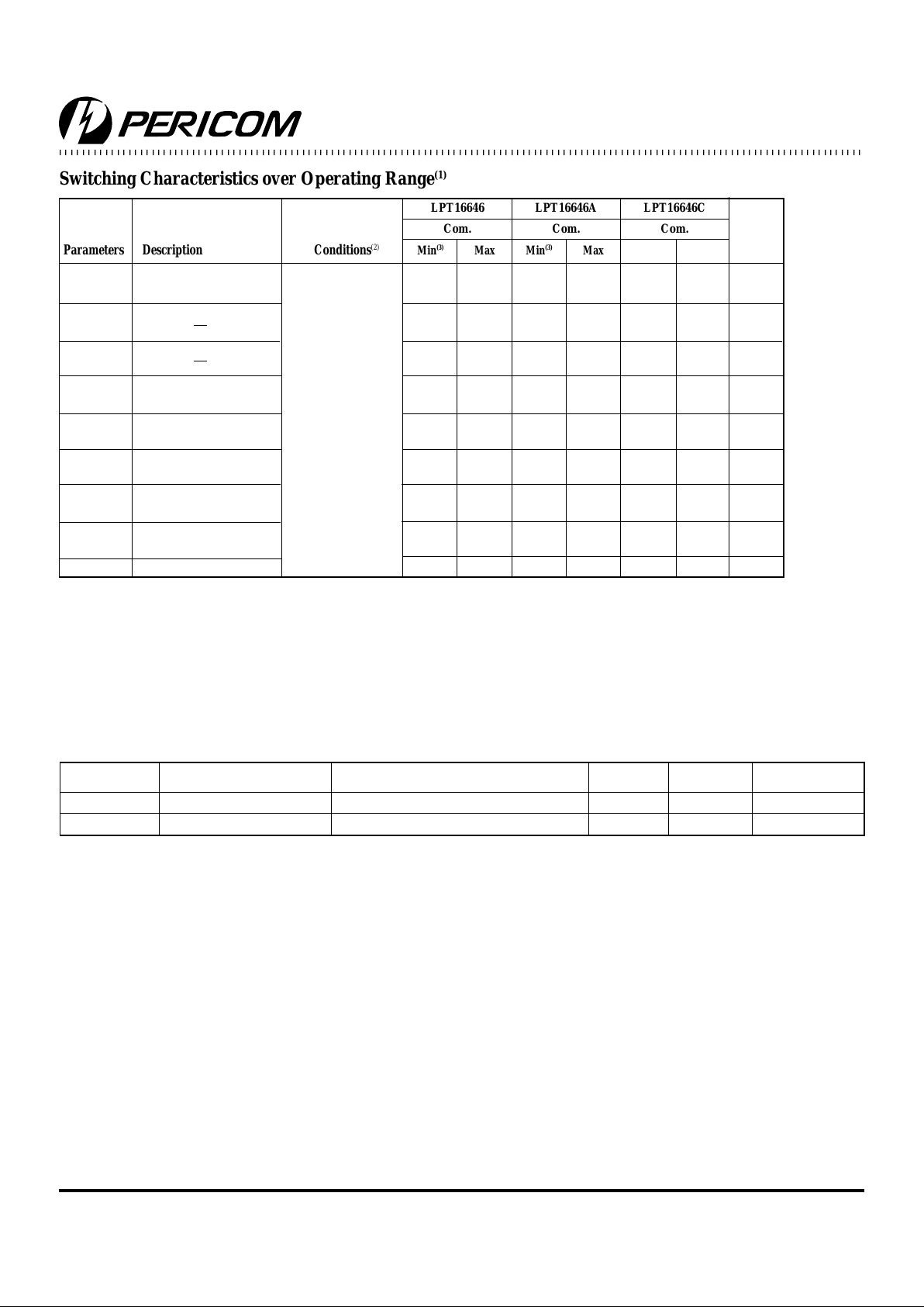
Switching Characteristics over Operating Range
(1)
LPT16646 LPT16646A LPT16646C
Com. Com. Com.
Parameters Description Conditions
(2)
Min
(3)
Max Min
(3)
Max Min
(3)
Max Unit
t
PLH
Propagation Delay CL = 50 pF 2.0 9.0 2.0 6.3 1.5 5.4 ns
t
PHL
Bus to Bus RL = 500
Ω
t
PZH
Output Enable Time 2.0 14.0 2.0 9.8 1.5 7.8 ns
t
PZL X
DIR or XOE to Bus
t
PHZ
Output Disable Time
(4)
2.0 9.0 2.0 6.3 1.5 6.3 ns
t
PLZ X
DIR or XOE to Bus
t
PLH
Propagation Delay 2.0 9.0 2.0 6.3 1.5 5.7 ns
t
PHL
Clock to Bus
t
PLH
Propagation Delay 2.0 11.0 2.0 7.7 1.5 6.2 ns
t
PHL
xSBA or xSAB to Bus
t
SU
Setup Time HIGH or 4.0 — 2.0 — 2.0 — ns
LOW, B
US
to Clock
t
H
Hold Time HIGH or 2.0 — 1. 5 — 1.5 — ns
LOW, Bus to Clock
t
W
Clock Pulse Width
(4)
6.0 — 5.0 — 5.0 — ns
HIGH or LOW
t
SK
(o) Output Skew
(5)
— 0.5 — 0.5 — 0.5 ns
Note:
1. This parameter is determined by device characterization but is not production tested.
Capacitance (TA = 25°C, f = 1 MHz)
Parameters
(1)
Description Test Conditions Typ Max. Units
CIN Input Capacitance VIN = 0V 4.5 6 pF
COUT Output Capacitance VOUT = 0V 5.5 8 pF
Notes:
1. Propagation Delays and Enable/Disable times are with Vcc = 3.3V ±0.3V, normal range. For Vcc = 2.7V, extended range,
all Propagation Delays and Enable/Disable times should be degraded by 20%.
2. See test circuit and wave forms.
3. Minimum limits are guaranteed but not tested on Propagation Delays.
4. This parameter is guaranteed but not production tested.
5. Skew between any two outputs, of the same package, switching in the same direction. This parameter is guaranteed by
design.
Pericom Semiconductor Corporation
2380 Bering Drive • San Jose, CA 95131 • 1-800-435-2336 • Fax (408) 435-1100 • http://www.pericom.com
 Loading...