

Page 1
1
PS8095B 10/07/98
12345678901234567890123456789012123456789012345678901234567890121234567890123456789012345678901212345678901234567890123456789012123456789012
1
234567890123456789012345678901212345678901234567890123456789012123456789012345678901234567890121234567890123456789012345678901212345678901
2
12345678901234567890123456789012123456789012345678901234567890121234567890123456789012345678901212345678901234567890123456789012123456789012
20-Bit Buffer Driver
with 3-STATE Outputs
PI74ALVCH162827
Product Description
Pericom Semiconductors PI74ALVCH series of logic circuits are
produced in the Companys advanced 0.5 micron CMOS
technology, achieving industry leading speed.
The PI74ALVCH162827 is a 20-bit non-inverting buffer/driver
designed for 2.3V to 3.6V VCC operation.
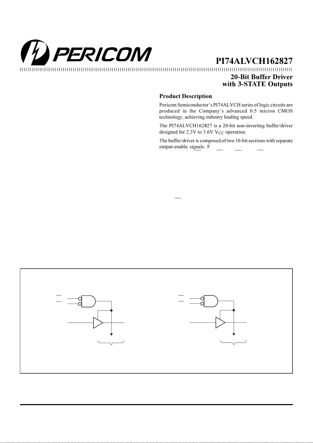
The buffer/driver is composed of two 10-bit sections with separate
output-enable signals. For either 10-bit buffer section, the two
output-enable (1OE1 and 1OE2 or 2OE1 and 2OE2) inputs must
both be low for the corresponding Y outputs to be active. If either
output-enable input is HIGH, the outputs of that 10-bit buffer
section are in the high-impedance state.
The outputs, which are designed to sink up to 12mA, include 26Ω
resistors to reduce overshoot and undershoot.
To ensure the high-impedance state during power up or power
down, OE should be tied to VCC through a pullup resistor; the
minimum value of the resistor is determined by the current-sinking
capability of the driver.
The PI74ALVCH162827 has Bus Hold which retains the data
inputs last state whenever the data input goes to high-impedance
preventing floating inputs and eliminating the need for pullup/
down resistors.
Product Features
• PI74ALVCH162827 is designed for low voltage operation
• V
CC
= 2.3V to 3.6V
• Hysteresis on all inputs
• Typical V
OLP
(Output Ground Bounce)
< 0.8V at VCC = 3.3V, TA = 25°C
• Typical V
OHV
(Output VOH Undershoot)
< 2.0V at VCC = 3.3V, TA = 25°C
• Output ports have equivalent 26Ω series resistors;
no external resistors are required
• Bus Hold retains last active bus state during 3-STATE,
eliminating the need for external pullup resistors
• Industrial operation at 40°C to +85°C
• Packages available:
56-pin 240 mil wide plastic TSSOP (A)
56-pin 300 mil wide plastic SSOP (V)
Logic Block Diagram
1
56
55
1
A1
1
OE2
1
OE1
1
Y1
2
To 9 Other Channels
28
29
42
2
A1
2
OE2
2
OE1
2
Y1
15
To 9 Other Channels
Page 2

PI74ALVCH162827
20-Bit Buffer Driver with 3-STATE Outputs
2
PS8095B 10/07/98
1OE1
1Y1
1Y2
GND
1Y3
1Y4
VCC
1Y5
1Y6
1Y7
GND
1Y8
1Y9
1Y10
2Y1
2Y2
2Y3
GND
2Y4
2Y5
2Y6
VCC
2Y7
2Y8
GND
2Y9
2Y10
2OE1
stupnIstuptuO
EO
1
EO
2
AY
LLL L
LLH H
HXX Z
XHX Z
Pin Name Description
OE Output Enable Input (Active LOW)
Ax Data Inputs
Yx 3-State Outputs
GND Ground
V
CC
Power
Product Pin Description Truth Table
(1)
Product Pin Configuration
Notes:
1. H = High Signal Level
L = Low Signal Level
X = Don't Care or Irrelevant
Z = High Impedance
1
2
3
4
5
6
7
8
9
10
11
12
13
14
15
16
17
18
19
20
21
22
23
24
56
55
54
53
52
51
50
49
48
47
46
45
44
43
42
41
40
39
38
37
36
35
34
33
25
26
27
28
32
31
30
29
56-PIN
V56
A56
1OE2
1A1
1A2
GND
1A3
1A4
VCC
1A5
1A6
1A7
GND
1A8
1A9
1A10
2A1
2A2
2A3
GND
2A4
2A5
2A6
VCC
2A7
2A8
GND
2A9
2A10
2OE2
Page 3

PI74ALVCH162827
20-Bit Buffer Driver with 3-STATE Outputs
3
PS8095B 10/07/98
Storage Temperature ............................................................ 65°C to +150°C
Ambient Temperature with Power Applied .......................... 40°C to +85°C
Input Voltage Range, V
IN
....................................................
0.5V to V
CC
+4.6V
Output Voltage Range, V
OUT
.............................................
0.5V to V
CC
+0.5V
DC Input Voltage ................................................................... 0.5V to +5.0V
DC Output Current ................................................................................ 50 mA
Power Dissipation ................................................................................... 1.0W
Note:
Stresses greater than those listed under MAXIMUM RATINGS
may cause permanent damage to the device. This is a stress rating
only and functional operation of the device at these or any other
conditions above those indicated in the operational sections of
this specification is not implied. Exposure to absolute maximum
rating conditions for extended periods may affect reliability.
DC Electrical Characteristics (Over the Operating Range, T
A
= 40°C to +85°C, VCC = 3.3V ±10%)
Maximum Ratings
(Above which the useful life may be impaired. For user guidelines, not tested.)
sretemaraPnoitpircseDsnoitidnoCtseT
)1(
.niM.pyT
)2(
.xaMstinU
V
CC
egatloVylppuS3.26.3
V
V
HI
)3(
egatloVHGIHtupnI
V
CC
V7.2otV3.2=7.1
V
CC
V6.3otV7.2=0.2
V
LI
)3(
egatloVWOLtupnI
V
CC
V7.2otV3.2=7.0
V
CC
V6.3otV7.2=8.0
V
NI
)3(
egatloVtupnI0V
CC
V
TUO
)3(
egatloVtuptuO0V
CC
V
HO
tuptuO
HGIH
egatloV
I
HO
001-= m V,A
CC
=.xaMot.niMV
CC
2.0-
V
HI
I,V7.1=
HO
4-=V,Am
CC
=V3.29.1
V
HI
I,V7.1=
HO
6-=V,Am
CC
=V3.27.1
V
HI
I,V0.2=
HO
6-=V,Am
CC
=V7.24.2
V
HI
I,V0.2=
HO
8-=V,Am
CC
=V0.30.2
V
HI
I,V0.2=
HO
21-=V,Am
CC
=V0.30.2
V
LO
tuptuO
WOL
egatloV
I
LO
001= m V,A
LI
=.xaMot.niM2.0
V
LI
I,V7.0=
LO
4=V,Am
CC
=V3.24.0
V
LI
I,V7.0=
LO
6=V,Am
CC
=V3.255.0
V
LI
I,V8.0=
LO
6=V,Am
CC
=V7.255.0
V
LI
I,V8.0=
LO
21=V,Am
CC
=V0.38.0
I
HO
)3(
tuptuO
HGIH
tnerruC
V
CC
V3.2=6-
Am
V
CC
V7.2=8-
V
CC
V0.3=21-
I
LO
)3(
tuptuO
WOL
tnerruC
V
CC
V3.2=6
V
CC
V7.2=8
V
CC
V0.3=21
Page 4

PI74ALVCH162827
20-Bit Buffer Driver with 3-STATE Outputs
4
PS8095B 10/07/98
sretemaraP)TUPNI(morF)TUPTUO(oT
V
CC
V2.0±V5.2=V
CC
V7.2=VCCV3.0±V3.3=
stinU
.niM
)2(
.xaM.niM
)2(
.xaM.niM
)2(
.xaM
t
DP
AY3.14.44.45.18.3
snt
NE
EOY5.12.72.66.12.5
t
SID
EOY4.29.52.58.17.4
noitpircseD
D /t Dv
)3(
llaFroesiRnoitisnarTtupnI001001001V/sn
Switching Characteristics over Operating Range
(1)
Pericom Semiconductor Corporation
2380 Bering Drive • San Jose, CA 95131 • 1-800-435-2336 • Fax (408) 435-1100 • http://www.pericom.com
Operating Characteristics, TA = 25ºC
retemaraPsnoitidnoCtseT
V
CC
V2.0±V5.2=VCCV3.0±V3.3=
stinU
.pyT
C
DP
noitapissiDrewoP
ecnaticapaC
delbanEstuptuO
C
L
zHM01=f,Fp05=
6181
Fp
delbasiDstuptuO46
Notes:
1. See test circuit and waveforms.
2. Minimum limits are guaranteed but not tested on Propagation Delays.
3. Recommended operating condition.
Notes:
1. For conditions shown as Max. or Min., use appropriate value specified under Electrical Characteristics for the applicable device type.
2. Typical values are at VCC = 3.3V, +25°C ambient and maximum loading.
3. Unused Control Inputs must be held HIGH or LOW to prevent them from floating.
DC Electrical Characteristics-Continued (Over the Operating Range, T
A
= 40°C to +85°C, VCC = 3.3V ±10%)
sretemaraPnoitpircseDsnoitidnoCtseT
)1(
.niM.pyT
)2(
.xaMstinU
I
NI
tnerruCtupnIV
NI
V=
CC
V,DNGro
CC
V6.3=5±
mA
I
NI
(
HOLD
)
tupnI
dloH
tnerruC
V
NI
V,V7.0=
CC
V3.2=54
V
NI
V,V7.1=
CC
V3.2=54-
V
NI
V,V8.0=
CC
V0.3=57
V
NI
V,V0.2=
CC
V0.3=57-
V
NI
0=otV,V6.3
CC
V6.3=005±
I
ZO
)stuptuOETATS-3(tnerruCtuptuOV
TUO
V=
CC
ro,DNGVCCV6.3=01±
I
CC
tnerruCylppuS
V
CC
=V6.3I,
TUO
0= m ,A
V
NI
VroDNG=
CC
04
DI
CC
tupnIreptnerruCylppuS
HGIHLTT@
V
CC
V0.3=ot6.3V
VtatupnIenO
CC
-V6.0
VtastupnIrehtO
CC
DNGro
057
C
I
stupnIlortnoC
V
NI
V=
CC
V,DNGro
CC
V3.3=
5.3
FpstupnIataD6
C
O
stuptuOV
O
V=
CC
V,DNGro
CC
V3.3=7
 Loading...