

Page 1
1
PS8088C 04/10/00
Product Description
Pericom Semiconductors PI74ALVCH series of logic circuits are
produced using the Companys advanced 0.5 micron CMOS
technology, achieving industry leading speed grades.
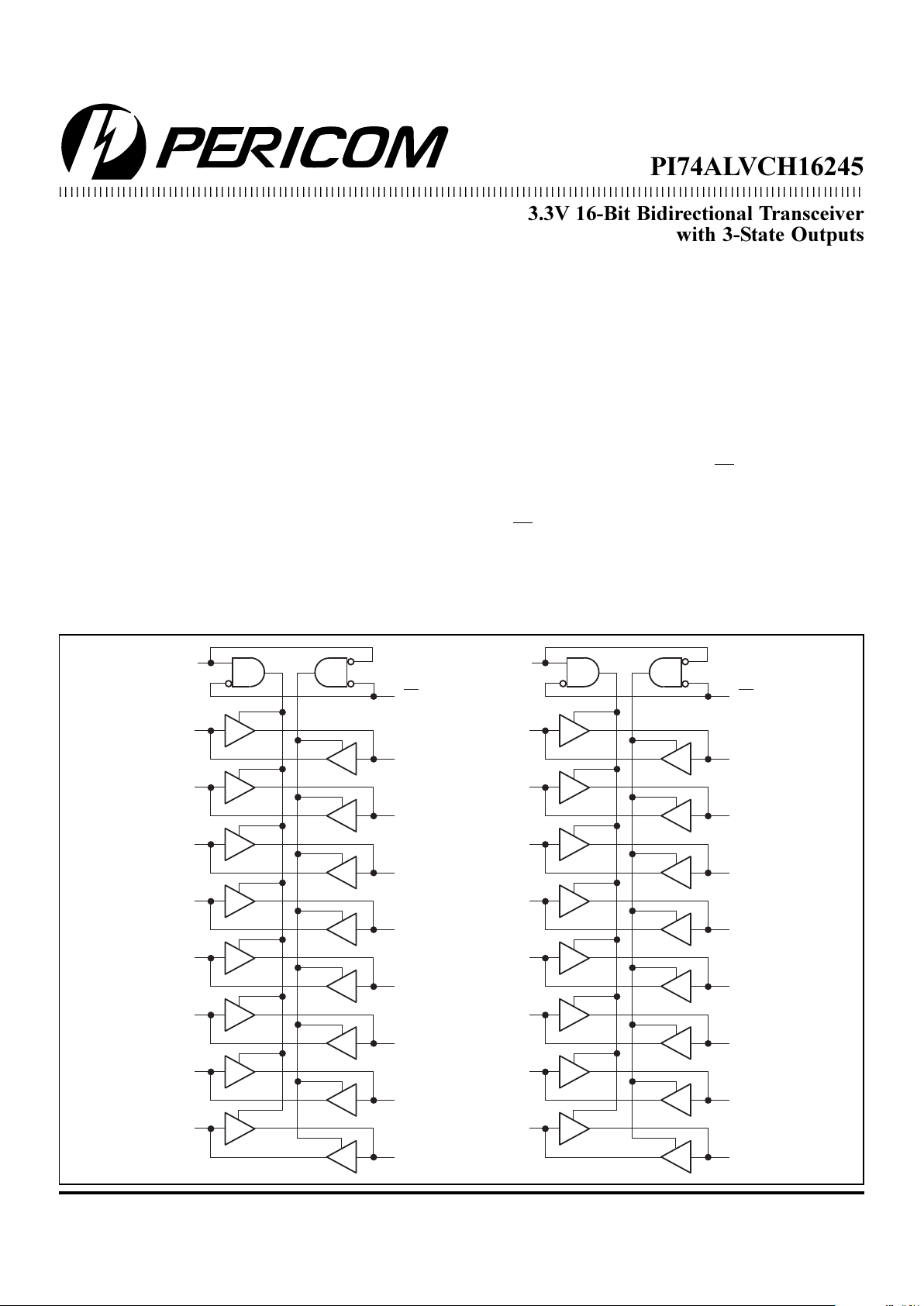
The PI74ALVCH16245 is a 16-bit bidirectional transceiver
designed for asynchronous two-way communication between
data buses. The direction control input pin (xDIR) determines
the direction of data flow through the bidirectional transceiver. The
Direction and Output Enable controls are designed to operate
this device as either two independent 8-bit transceivers or one
16-bit transceiver. The output enable (OE) input, when HIGH,
disables both A and B ports by placing them in HIGH Z condition.
To ensure the high-impedance state during power up or power
down, OE should be tied to VCC through a pull-up resistor; the
minimum value of the resistor is determined by the current sinking
ability of the driver.
Active bus-hold circuitry is provided to hold unused or floating
data inputs at a valid logic level.
Product Features
• PI74ALVCH16245 is designed for low voltage operation
• V
CC
= 2.3V to 3.6V
• Hysteresis on all inputs
• Typical V
OLP
(Output Ground Bounce)
< 0.8V at VCC = 3.3V, TA = 25°C
• Typical V
OHV
(Output VOH Undershoot)
< 2.0V at VCC = 3.3V, TA = 25°C
• Bus Hold retains last active bus state during 3-STATE,
eliminating the need for external pullup resistors
• Industrial operation at 40°C to +85°C
• Packages available:
48-pin 240 mil wide plastic TSSOP (A)
48-pin 300 mil wide plastic SSOP (V)
Logic Block Diagram
1B0
1A0
1
OE
1
DIR
1B1
1A1
1B2
1A2
1B3
1A3
1B4
1A4
1B5
1A5
1B6
1A6
1B7
1A7
2B0
2A0
2
OE
2
DIR
2B1
2A1
2B2
2A2
2B3
2A3
2B4
2A4
2B5
2A5
2B6
2A6
2B7
2A7
12345678901234567890123456789012123456789012345678901234567890121234567890123456789012345678901212345678901234567890123456789012123456789012
1
234567890123456789012345678901212345678901234567890123456789012123456789012345678901234567890121234567890123456789012345678901212345678901
2
12345678901234567890123456789012123456789012345678901234567890121234567890123456789012345678901212345678901234567890123456789012123456789012
3.3V 16-Bit Bidirectional Transceiver
with 3-State Outputs
PI74ALVCH16245
Page 2
2
PS8088C 04/10/00
PI74ALVCH16245
3.3V 16-Bit Bidirectional Tranceiver
with 3-State Outputs
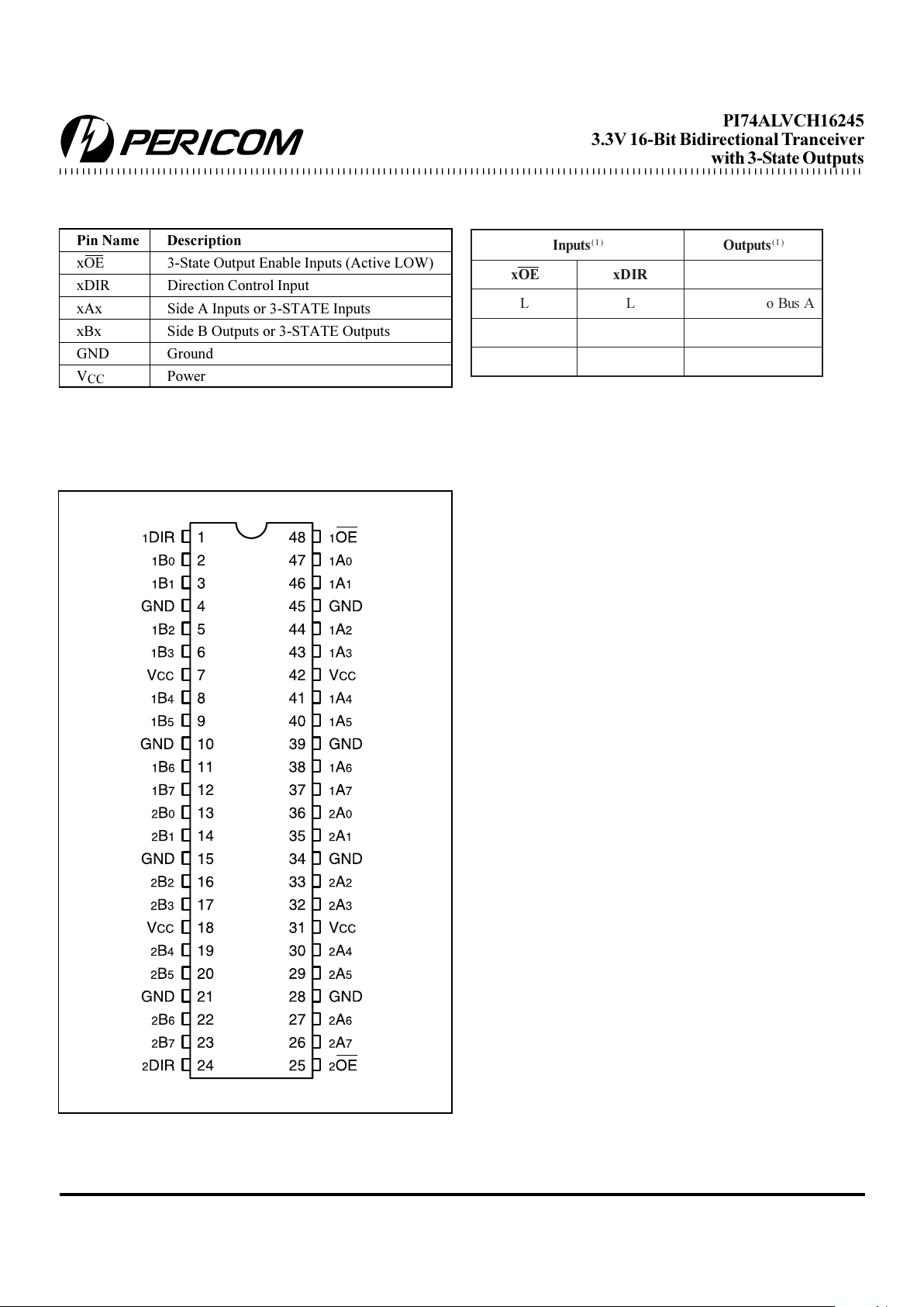
Pin Name Description
xOE 3-State Output Enable Inputs (Active LOW)
xDIR Direction Control Input
xAx Side A Inputs or 3-STATE Inputs
xBx Side B Outputs or 3-STATE Outputs
GND Ground
V
CC
Power
stupnI
)1(
stuptuO
)1(
EOxRIDx
LL AsuBotataDBsuB
LH BsuBotataDAsuB
HX Z
Product Pin Description Truth Table
(1)
Product Pin Configuration
Notes:
1. H = High Voltage Level
L = Low Voltage Level
X = Don't Care
Z = High Impedance
48-pin
A, V
Page 3
PI74ALVCH16245
3.3V 16-Bit Bidirectional Tranceiver
with 3-State Outputs
3
PS8088C 04/10/00
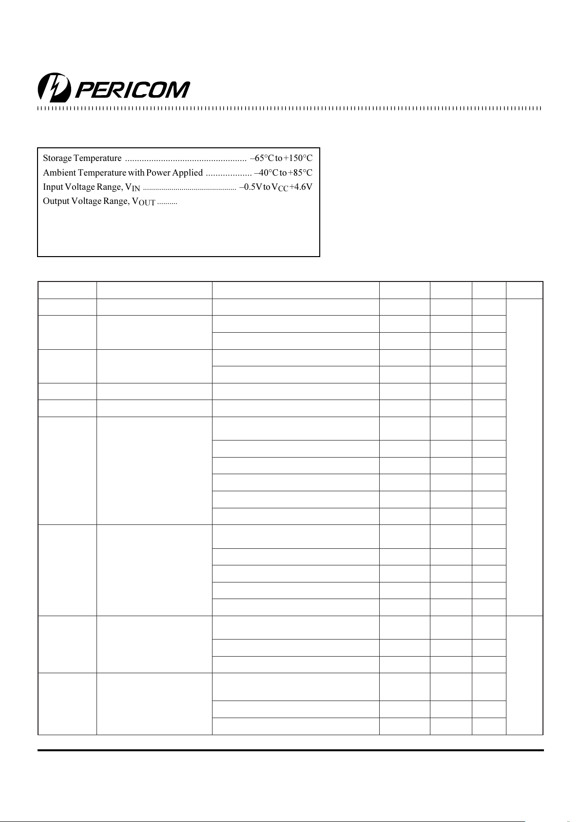
Storage Temperature ................................................... 65°C to +150°C
Ambient Temperature with Power Applied ................... 40°C to +85°C
Input Voltage Range, V
IN
..............................................
0.5V to V
CC
+4.6V
Output Voltage Range, V
OUT
.......................................
0.5V to V
CC
+0.5V
DC Input Voltage ............................................................ 0.5V to +5.0V
DC Output Current ....................................................................... 50 mA
Power Dissipation .......................................................................... 1.0W
Note:
Stresses greater than those listed under MAXIMUM
RATINGS may cause permanent damage to the device.
This is a stress rating only and functional operation of the
device at these or any other conditions above those
indicated in the operational sections of this specification
is not implied. Exposure to absolute maximum rating
conditions for extended periods may affect reliability.
DC Electrical Characteristics (Over the Operating Range, T
A
= 40°C to +85°C, VCC = 3.3V ±10%)
Maximum Ratings
(Above which the useful life may be impaired. For user guidelines, not tested.)
sretemaraPnoitpircseDsnoitidnoCtseT
)1(
.niM.pyT
)2(
.xaMstinU
V
CC
egatloVylppuS3.26.3
V
V
HI
)3(
egatloVHGIHtupnI
V
CC
V7.2otV3.2=7.1
V
CC
V6.3otV7.2=0.2
V
LI
)3(
egatloVWOLtupnI
V
CC
V7.2otV3.2=7.0
V
CC
V6.3otV7.2=8.0
V
NI
)3(
egatloVtupnI0V
CC
V
TUO
)3(
egatloVtuptuO0V
CC
V
HO
tuptuO
HGIH
egatloV
I
HO
001-= µ V,A
CC
=.xaMot.niMV
CC
2.0-
V
HI
I,V7.1=
HO
6-=V,Am
CC
=V3.20.2
V
HI
I,V7.1=
HO
21-=V,Am
CC
=V3.27.1
V
HI
I,V0.2=
HO
21-=V,Am
CC
=V7.22.2
V
HI
I,V0.2=
HO
21-=V,Am
CC
=V0.34.2
V
HI
I,V0.2=
HO
42-=V,Am
CC
=V0.30.2
V
LO
tuptuO
WOL
egatloV
I
LO
001= µ V,A
LI
=.xaMot.niM2.0
V
LI
I,V7.0=
LO
6=V,Am
CC
=V3.24.0
V
LI
I,V7.0=
LO
21=V,Am
CC
=V3.27.0
V
LI
I,V8.0=
LO
21=V,Am
CC
=V7.24.0
V
LI
I,V8.0=
LO
42=V,Am
CC
=V0.355.0
I
HO
)3(
tuptuO
HGIH
tnerruC
V
CC
V3.2=21
Am
V
CC
V7.2=21
V
CC
V0.3=42
I
LO
)3(
tuptuO
WOL
tnerruC
V
CC
V3.2=21
V
CC
V7.2=21
V
CC
V0.3=42
Page 4
4
PS8088C 04/10/00
PI74ALVCH16245
3.3V 16-Bit Bidirectional Tranceiver
with 3-State Outputs
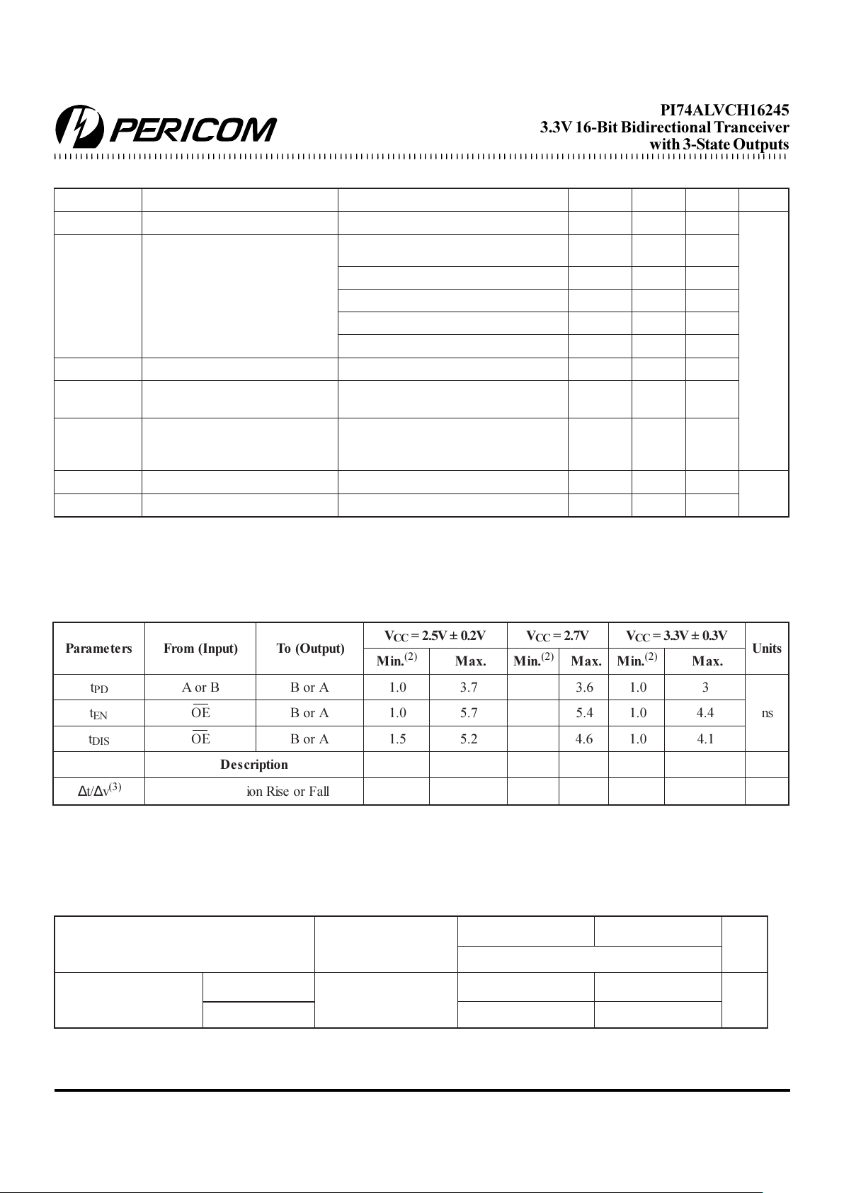
sretemaraP)tupnI(morF)tuptuO(oT
V
CC
V2.0±V5.2=V
CC
V7.2=VCCV3.0±V3.3=
stinU
.niM
)2(
.xaM.niM
)2(
.xaM.niM
)2(
.xaM
t
DP
BroAAroB0.17.36.30.13
snt
NE
EOAroB0.17.54.50.14.4
t
SID
EOAroB5.12.56.40.11.4
noitpircseD
∆ /t ∆v
)3(
llaFroesiRnoitisnarTtupnI0010010 01V/sn
Switching Characteristics over Operating Range
(1)
Pericom Semiconductor Corporation
2380 Bering Drive • San Jose, CA 95131 • 1-800-435-2336 • Fax (408) 435-1100 • http://www.pericom.com
Operating Characteristics, TA = 25ºC
retemaraPsnoitidnoCtseT
V
CC
V2.0±V5.2=VCCV3.0±V3.3=
stinU
lacipyT
C
DP
noitapissiDrewoP
ecnaticapaC
delbanEstuptuO
C
L
Fp05=
zHM01=f
2292
Fp
delbasiDstuptuO45
Notes:
1. See test circuit and waveforms.
2. Minimum limits are guaranteed but not tested on Propagation Delays.
3. Recommended operating condition.
Notes:
1. For Max. or Min. conditions, use appropriate value specified under Electrical Characteristics for the applicable device type.
2. Typical values are at VCC = 3.3V, +25°C ambient and maximum loading.
3. Unused Control Inputs must be held HIGH or LOW to prevent them from floating.
DC Electrical Characteristics-Continued (Over the Operating Range, T
A
= 40°C to +85°C, VCC = 3.3V ±10%)
sretemaraPnoitpircseDsnoitidnoCtseT
)1(
.niM.pyT
)2(
.xaMstinU
I
NI
tnerruCtupnIV
NI
V=
CC
V,DNGro
CC
V6.3=5±
µA
I
NI
(
HOLD
)
tupnI
dloH
tnerruC
V
NI
V,V7.0=
CC
V3.2=54
V
NI
V,V7.1=
CC
V3.2=54
V
NI
V,V8.0=
CC
V0.3=57
V
NI
V,V0.2=
CC
V0.3=57
V
NI
0=otV,V6.3
CC
V6.3=005±
I
ZO
)stuptuOETATS-3(tnerruCtuptuOV
TUO
V=
CC
ro,DNGVCCV6.3=01±
I
CC
tnerruCylppuS
V
CC
=V6.3I,
TUO
0= µ ,A
V
NI
VroDNG=
CC
04
∆I
CC
tupnIreptnerruCylppuS
HGIHLTT@
V
CC
V0.3=ot6.3V
VtatupnIenO
CC
-V6.0
VtastupnIrehtO
CC
DNGro
057
C
I
stupnIlortnoCV
NI
V=
CC
V,DNGro
CC
V3.3=4
Fp
C
OI
stroPBroAV
O
V=
CC
V,DNGro
CC
V3.3=7
 Loading...