

Page 1
12345678901234567890123456789012123456789012345678901234567890121234567890123456789012345678901212345678901234567890123456789012123456789012
12345678901234567890123456789012123456789012345678901234567890121234567890123456789012345678901212345678901234567890123456789012123456789012
12345678901234567890123456789012123456789012345678901234567890121234567890123456789012345678901212345678901234567890123456789012123456789012
Product Features
Near-zero propagation delay
Low noise, 25Ω version (PI5C32383)
5Ω switches connect inputs to outputs (PI5C3383)
Direct bus connection when switches are ON
Ultra-low quiescent power (0.2µA typical)
Ideally suited for notebook applications
Packages available:
24-pin 173-mil wide plastic TSSOP (L)
24-pin 150-mil wide plastic QSOP (Q)
24-pin 300-mil wide plastic SOIC (S)
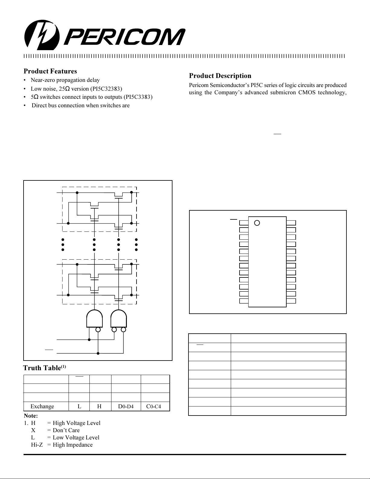
Logic Block Diagram
PI5C3383/PI5C32383
5-Bit, 4-Port Bus Exchange Switch
PI5C3383
PI5C32383 (25
ΩΩ
Ω)
ΩΩ
5-Bit, 4-Port Bus Exchange Switch
Product Description
Pericom Semiconductors PI5C series of logic circuits are produced
using the Companys advanced submicron CMOS technology,
achieving industry leading performance.
The PI5C3383 and PI5C32383 are 5-bit, 4-port bus switch with
exchange designed with a low ON resistance allowing inputs to be
connected directly to outputs. The bus switch creates no additional
propagational delay or additional ground bounce noise. The switches
are turned ON by the Bus Enable (BE) input signal, and the Bus
Exchange (BX) input signal offers nibble swapping of the AB and
CD pairs of signals. This exchange configuration allows byte
swapping of buses in systems. It can also be used as a quad
2-to-1 multiplexer and to create low delay barrel shifters, etc. The
PI5C32383 is designed with an internal 25Ω resistor reducing noise
reflection in high-speed applications.
A0
B0
A4
B4
BX
BE
Truth Table
(1)
Function BE BX A0-A4 B0-B4
Disconnect H X Hi-Z Hi-Z
Connect L L C0-C4 D0-D4
Exchange L H D0-D4 C0-C4
Note:
1. H = High Voltage Level
X = Dont Care
L = Low Voltage Level
Hi-Z = High Impedance
C0
D0
C4
D4
Product Pin Configuration
BE
C
A
B
D
C
A
B
D
C
A
GND
1
2
0
3
0
4
0
0
1
1
1
1
2
2
5
6
7
8
9
10
11
12
24-Pin
L, Q, S
24
23
22
21
20
19
18
17
16
15
14
13
Product Pin Description
Pin Name Description
BE Bus Enable Input (Active LOW)
BX Bus Exchange Input
Ax Bus A
Bx Bus B
Cx Bus C
Dx Bus D
GND Ground
V
CC
Power
Vcc
D
4
B
4
A
4
C
4
D
3
B
3
A
3
C
3
D
2
B
2
BX
1
PS7028C 05/19/00
Page 2

12345678901234567890123456789012123456789012345678901234567890121234567890123456789012345678901212345678901234567890123456789012123456789012
Maximum Ratings
(Above which the useful life may be impaired. For user guidelines, not tested.)
PI5C3383/PI5C32383
5-Bit, 4-Port Bus Exchange Switch
Storage Temperature ........................................................–65°C to +150°C
Ambient Temperature with Power Applied ....................... –40°C to +85°C
Supply Voltage to Ground Potential (Inputs & Vcc Only) .–0.5V to +7.0V
Supply Voltage to Ground Potential (Outputs & D/O Only)–0.5V to +7.0V
DC Input Voltage ................................................................ –0.5V to +7.0V
DC Output Current .......................................................................... 120 mA
Power Dissipation................................................................................ 0.5W
DC Electrical Characteristics (Over the Operating Range, T
= –40°C to +85°C, VCC = 5V ±5%)
A
Parameters Description Test Conditions
V
V
I
IH
I
IL
I
OZH
V
I
OS
V
R
IH
IL
IK
H
ON
Input HIGH Voltage Guaranteed Logic HIGH Level 2.0 — — V
Input LOW Voltage Guaranteed Logic LOW Level –0.5 — 0.8 V
Input HIGH Current VCC = Max., VIN = V
Input LOW Current VCC = Max., VIN = GND — — ±1 µA
High Impedance Output Current 0 ≤ AB, CD ≤ V
CC
Clamp Diode Voltage VCC = Min., IIN = –18mA — –0.7 –1.2 V
Short Circuit Current
(3)
AB (CD) = 0V, CD (AB) = V
Input Hysteresis at Control Pins — 150 — mV
Switch On Resistance
(4)
VCC = Min., VIN = 0.0V, PI5C3383 — 5 7 Ω
ION = 48mA PI5C32383 15 2 0 40
Note:
Stresses greater than those listed under MAXIMUM
RATINGS may cause permanent damage to the device. This is a stress rating only and functional operation of the device at these or any other conditions above
those indicated in the operational sections of this
specification is not implied. Exposure to absolute
maximum rating conditions for extended periods may
affect reliability.
(1)
CC
Min. Typ
——±1µA
(2)
Max. Units
——±1µA
CC
100 — — mA
VCC = Min., VIN = 2.4V, PI5C3383 — 10 15 Ω
ION = 15mA PI5C32383 15 2 5 48
Capacitance (T
Parameters
C
IN
C
OFF
C
ON
= 25°C, f = 1 MHz)
A
(5)
Description Test Conditions Typ Max. Units
Input Capacitance VIN = 0V — 6 pF
AB/CD Capacitance, Switch Off VIN = 0V — 6 pF
AB/CD Capacitance, Switch On VIN = 0V — 8 pF
Notes:
1. For Max. or Min. conditions, use appropriate value specified under Electrical Characteristics for the applicable device type.
2. Typical values are at VCC = 5.0V, TA = 25°C ambient and maximum loading.
3. Not more than one output should be shorted at one time. Duration of the test should not exceed one second.
4. Measured by the voltage drop between AB and CD pin at indicated current through the switch. ON resistance is determined by
the lower of the voltages on the two (A or B, C or D) pins.
5. This parameter is determined by device characterization but is not production tested.
2
PS7028C 05/19/00
Page 3

PI5C3383/PI5C32383
12345678901234567890123456789012123456789012345678901234567890121234567890123456789012345678901212345678901234567890123456789012123456789012
5-Bit, 4-Port Bus Exchange Switch
Power Supply Characteristics
Parameters Description Test Conditions
(1)
Min. Typ
ICC Quiescent Power VCC = Max. VIN = GND or VCC — 0.1 3.0 µA
Supply Current
∆ICC Supply Current per VCC = Max. VIN = 3.4V
(3)
— — 2.5 mA
Input @ TTL HIGH
(2)
Max. Units
ICCD Supply Current per VCC = Max., — — 0.25 mA/
Input per MHz
(4)
AB and CD Pins Open MHz
BE = GND
Control Input Toggling
50% Duty Cycle
Notes:
1. For Max. or Min. conditions, use appropriate value specified under Electrical Characteristics for the applicable device.
2. Typical values are at Vcc = 5.0V, +25°C ambient.
3. Per TTL driven input (VIN = 3.4V, control inputs only); A, B, C, and D pins do not contribute to Icc.
4. This current applies to the control inputs only and represent the current required to switch internal capacitance at the specified
frequency. The A, B, C, and D inputs generate no significant AC or DC currents as they transition. This parameter is not tested,
but is guaranteed by design.
PI5C3383 Switching Characteristics over Operating Range
PI5C3383
Com
Parameters Description Conditions
tPLH Propagation Delay
(2,3)
CL = 50 pF — 0.25 — ns
tPHL Ax to Cx, Bx to Dx RL = 500Ω
tPZH Bus Enable Time 1.5 — 6.5 ns
tPZL BE to Cx or Dx
tPHZ Bus Disable Time 1.5 — 5.5 ns
tPLZ BE to Cx or Dx
tBX Bus Exchange Time 1.5 — 6.5 ns
BX to Cx or Dx
(1)
Min T yp Max Unit
Notes:
1. See test circuit and waveforms.
2. This parameter is guaranteed but not tested on Propagation Delays.
3. The bus switch contributes no propagational delay other than the RC delay of the ON resistance of the switch and the load
capacitance. The time constant for the switch alone is of the order of 0.25\ns for 50pF load. Since this time constant is much
smaller than the rise/fall times of typical driving signals, it adds very little propagational delay to the system. Propagational delay
of the bus switch when used in a system is determined by the driving circuit on the driving side of the switch and its interaction
with the load on the driven side.
3
PS7028C 05/19/00
Page 4

PI5C3383/PI5C32383
12345678901234567890123456789012123456789012345678901234567890121234567890123456789012345678901212345678901234567890123456789012123456789012
5-Bit, 4-Port Bus Exchange Switch
PI5C32383 Switching Characteristics over Operating Range
PI5C32383
Com
Parameters Description Conditions
tPLH Propagation Delay
(2,3)
CL = 50pF 1.25 ns
tPHL Ax to Cx, Bx to Dx RL = 500Ω
tPZH Bus Enable Time 1.5 6.5 ns
tPZL BE to Cx or Dx
tPHZ Bus Disable Time 1.5 5.5 ns
tPLZ BE to Cx or Dx
tBX Bus Exchange Time 1.5 6.5 ns
BX to Cx or Dx
Notes:
1. See test circuit and waveforms.
2. This parameter is guaranteed but not tested on Propagation Delays.
3. The bus switch contributes no propagational delay other than the RC delay of the ON resistance of the switch and the load
capacitance. The time constant for the switch alone is of the order of 0.25ns for 50pF load. Since this time constant is much
smaller than the rise/fall times of typical driving signals, it adds very little propagational delay to the system. Propagational delay
of the bus switch when used in a system is determined by the driving circuit on the driving side of the switch and its interaction
with the load on the driven side.
(1)
Min Typ Max Units
Applications
Logic Inputs
The logic control inputs can be driven up to +5.5V regardless of the supply voltage. For example, given a 5.0V supply, the control
or select pins may be driven low to 0V and high to 5.5V. Driving the control or select pins Rail-toRail minimizes power
consumption.
Power-Supply Sequencing
Proper power-supply sequencing is recommended for all CMOS devices. Always apply VCC before applying signals to the input/
output or control pins.
Ordering Information
traPegakcaP-niPerutarepmeT
L3833C5IP)L(POSST42
Q3833C5IP)Q(POSQ42
S3833C5IP)S(CIOS42
C°58+otC°04
4
PS7028C 05/19/00
Page 5
12345678901234567890123456789012123456789012345678901234567890121234567890123456789012345678901212345678901234567890123456789012123456789012
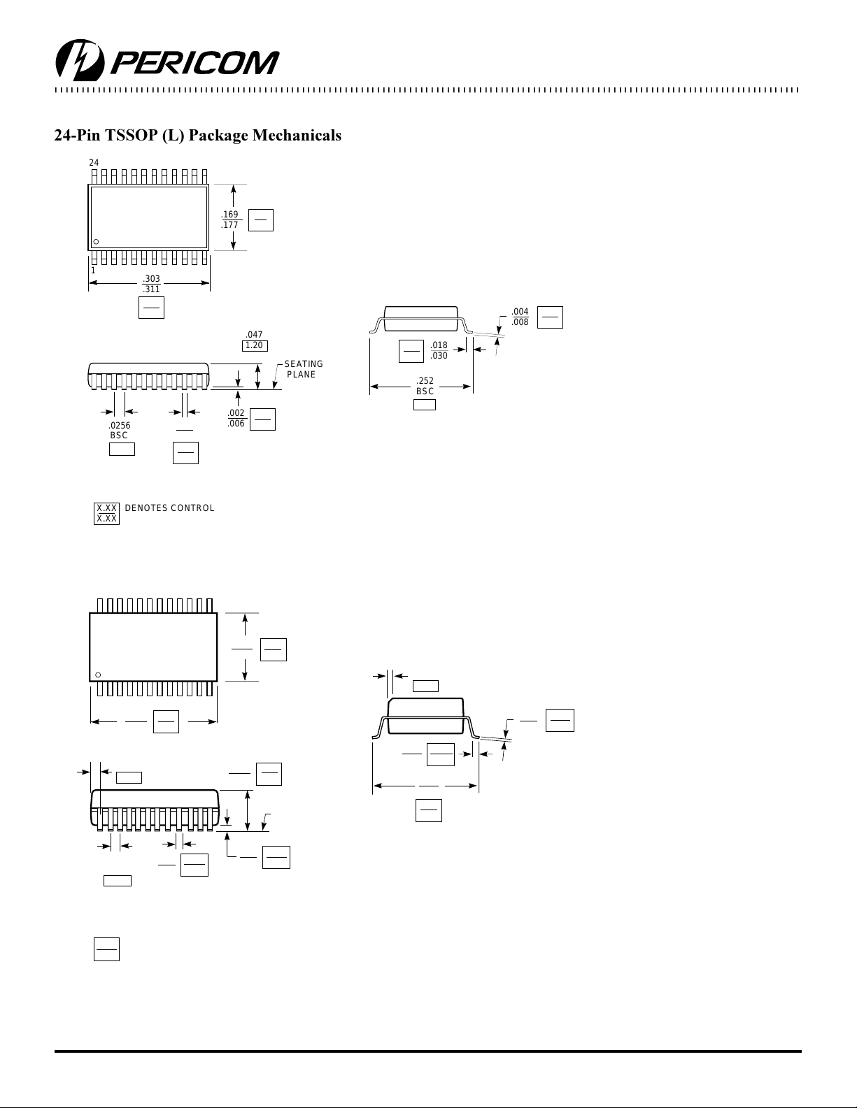
24-Pin TSSOP (L) Package Mechanicals
24
.169
4.3
.177
4.5
PI5C3383/PI5C32383
5-Bit, 4-Port Bus Exchange Switch
1
X.XX
X.XX
.303
.311
7.7
7.9
.0256
BSC
0.65
DENOTES CONTROLLING
DIMENSIONS IN MILLIMETERS
.007
.012
0.19
0.30
.002
.006
.047
1.20
Max
0.05
0.15
SEATING
PLANE
24-Pin QSOP (Q) Package Mechanicals
24
.150
3.81
.157
3.99
1
8.56
.337
.344
8.74
.033
0.84
.053
.069
1.35
1.75
SEATING
PLANE
0.45
0.75
.252
BSC
6.4
.015 x 45˚
0.38
.016
.050
.228
.244
5.79
6.20
.018
.030
0.406
1.27
.004
.008
.007
.010
0.09
0.20
0.178
0.254
0.101
.025
typical
0.635
X.XX
DENOTES DIMENSIONS
X.XX
IN MILLIMETERS
.008
.012
0.203
0.305
.004
.010
0.254
5
PS7028C 05/19/00
Page 6
12345678901234567890123456789012123456789012345678901234567890121234567890123456789012345678901212345678901234567890123456789012123456789012
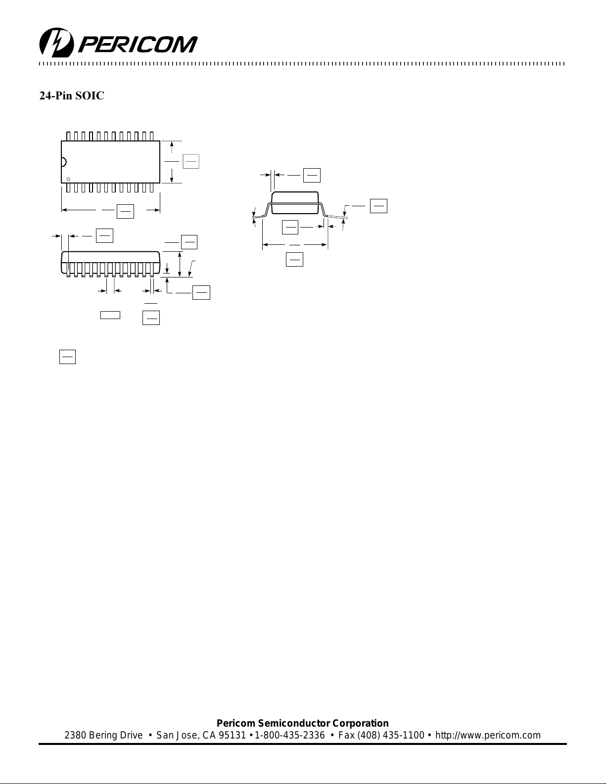
24-Pin SOIC (S) Package Mechanicals
24
7.40
.2914
7.60
.2992
.010
.029
0.254
0.737
PI5C3383/PI5C32383
5-Bit, 4-Port Bus Exchange Switch
x 45˚
1
0.533
.021
0.787
.031
X.XX
DENOTES DIMENSIONS
X.XX
IN MILLIMETERS
.5985
.6141
.050
BSC
1.27
15.20
15.60
.013
.020
0.33
0.51
.0926
.1043
.0040
.0118
2.35
2.65
SEATING
PLANE
0.10
0.30
0-8˚
0.41
1.27
.394
.419
10.00
10.65
.016
.050
.0091
.0125
0.23
0.32
Pericom Semiconductor Corporation
2380 Bering Drive • San Jose, CA 95131 • 1-800-435-2336 • Fax (408) 435-1100 • http://www.pericom.com
6
PS7028C 05/19/00
 Loading...