

Page 1
Key Features
• 1550 nm DFB CW source monolithicly
integrated with an Electro Absorptionmodulator (EA)
• Hermetic, 7 pin butterfly package
• Single-mode fiber pigtail
• 12 GHz typical bandwidth
• -3 dBm output power
• Multisourced footprint
Applications
• DWDM SDH STM-64 LH
• DWDM SONET OC-192 LR
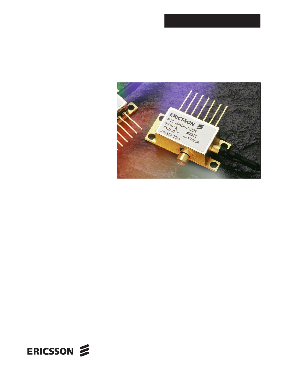
PGT 204 04
DFB/EA Laser Module
for 10 Gb/s Applications
Description
The laser module, intended for OC-192/STM-64 DWDM applications, consists of a DFB laser with integrated absorption modulator mounted in a high
frequency package which includes an isolator. Laser wavelengths are
available according to the ITU-T grid.
1
Page 2
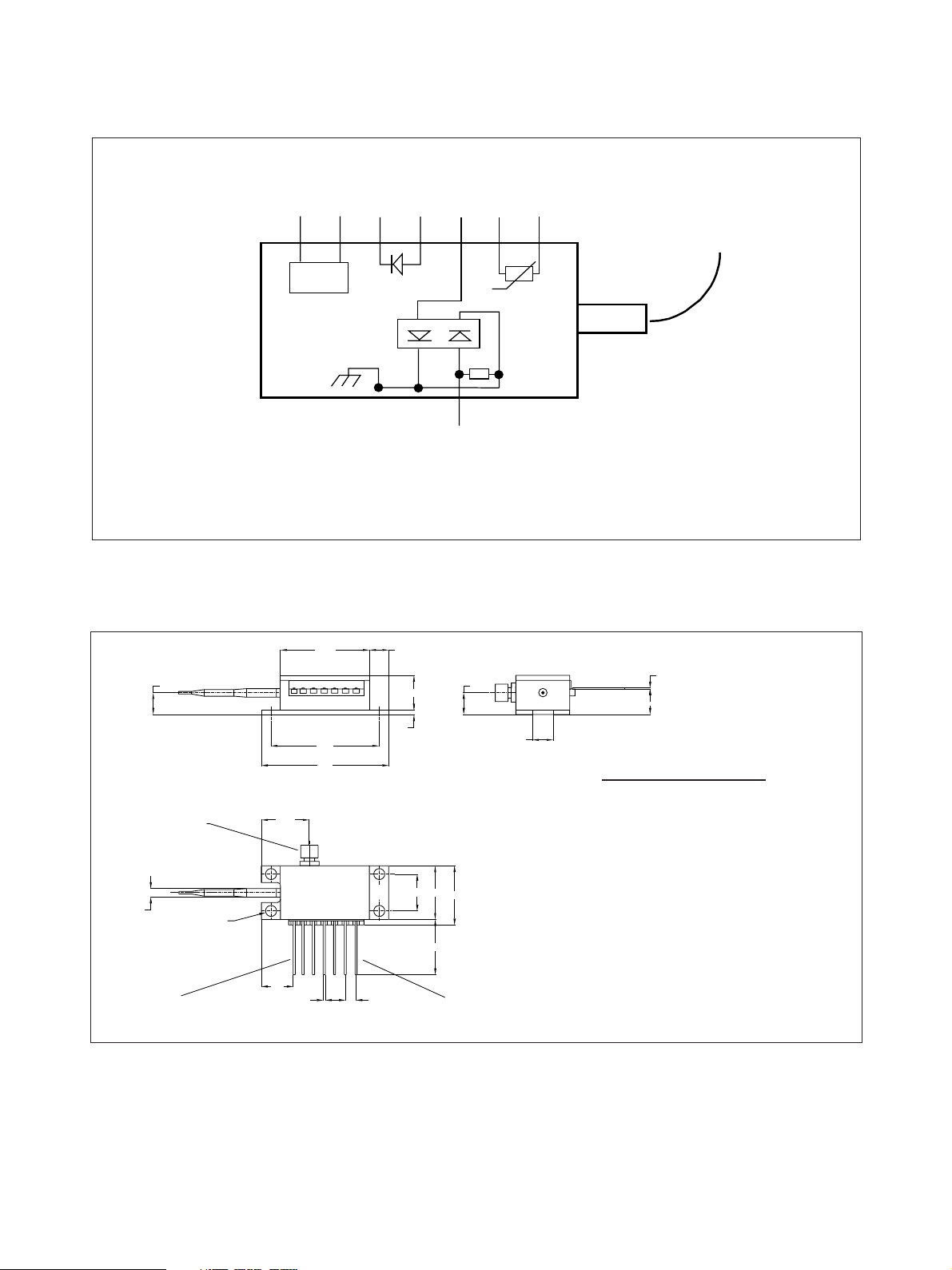
PGT 204 04
71
10k
TEC
8
TOP VIEW
Figure 1. Block diagram
5.0
Pin 8
ø3.0
Pin 1
4xø2.6
20.83
26.4
30.0
4.5
8.2
1.0
5.1
5.0
0.2
5.8
Pin Description
1. Thermistor
12.02
2. Thermistor
3. Laser DC bias (+)
4. Monitor (-)
5. Monitor (+)
8.89
12.7
14.0
6. TEC (+)
7. TEC (-)
8. EA modulation (-)
Min. 10
7.3
7x0.5
6x2.54
Pin 7
Figure 2. Pin description
2
Page 3

PGT 204 04
Optical Characteristics
Electrical and optical characteristics at recommended operating conditions, unless otherwise noted.
Parameter Conditions Symbol Min Typ Max Unit
Wavelength ITU-T grid λ 1530 1564 nm
Output power BOL P
Extinction ratio 2.5 V
pp
Out
ER 10 dB
Dispersion penalty @ 800 ps/nm disp. 1.5 dB
Side mode suppr.ratio SMSR 35 dB
Optical isolation 30 dB
Electrical Characteristics
Parameter Conditions Symbol Min Typ Max Unit
Operating current I
Threshold current I
Forward voltage V
Reflection, S
11
0 - 5 GHz -12 dB
5 – 9 GHz -9 dB
Small signal modulation bandwidth -3 dB
e
Rise/Fall time 10/90% tr/t
Monitor current I
Monitor dark current -5 V 5 100 nA
Thermistor resistance @ 25 °C 9.5 10.5 kΩ
TEC Voltage -2.5 2.5 V
Current -1.2 1.2 A
Power 3W
f
Op
th
f
c
f
Mon
-3 dBm
50 100 mA
25 mA
2V
12 GHz
40 ps
0.1 1 mA
Operating Conditions
Parameter Symbol Min Typ Max Unit
Operating case temperature T
Operating chip temperature T
Case
Op
070°C
20 35 °C
Absolute Maximum Ratings
Parameter Symbol Min Max Unit
Storage temperature T
Laser forward current I
Modulator voltage V
Stg
LD
Mod
CAUTION: Stresses outside those listed in ”Absolute Maximum Ratings” may cause permanent damage to the device.
-40 85 °C
150 mA
-4 1 V
3
Page 4

PGT 204 04
Handling Precautions
This device may be damaged as a result of electrostatic
discharge (ESD). Take proper precautions during both handling and testing. This typically includes grounded wrist
wraps, workbenches and floor mats in ESD controlled areas.
Semiconductor devices may be damaged by current surges,
use appropriate transient protection.
Quality Assurance
Ericsson Microelectronics commitment to quality has been
proven through a decade of semiconductor device production and has been confirmed to ISO 9001. Opto product
qualification is made according to the intention of applicable
Telcordia standards.
Connector Options
FC/PC
SC
(Other connectors available on request)
DANGER
DANGER
INVISIBLE LASER RADIATION
AVOID DIRECT EXPOSURE TO BEAM
WAVELENGTH 1300 nm - 1600 nm
CLASS 3B LASER
Information given in this data sheet is believed to be accurate and
reliable. However no responsibility is assumed for the consequences of
its use nor for any infringement of patents or other rights of third
parties which may result from its use. No license is granted by
implication or otherwise under any patent or patent rights of Ericsson
Microelectronics. These products are sold only according to Ericsson
Microelectronics' general conditions of sale, unless otherwise
confirmed in writing.
Product specifications subject to change without
notice.
Ericsson Microelectronics AB
SE-164 81 Kista, Sweden
Telephone: +46 8 757 50 00
www.ericsson.com/microelectronics
For local sales contacts, please refer to our website
or call: Int + 46 8 757 47 00, Fax: +46 8 757 47 76
1522-PGT 204 04 Rev. E
© Ericsson Microelectronics AB, October 2000
4
 Loading...