

Page 1
®
®
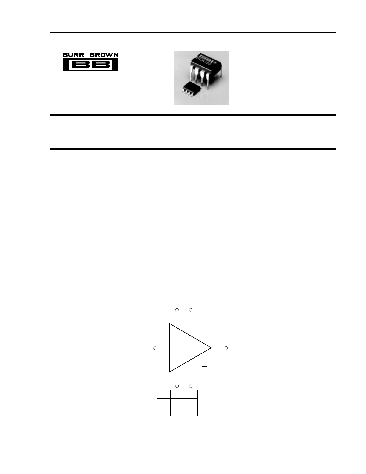
PGA103
Programmable Gain
AMPLIFIER
FEATURES
● DIGITALLY PROGRAMABLE GAINS:
G=1, 10, 100V/V
● CMOS/TTL-COMPATIBLE INPUTS
● LOW GAIN ERROR:
● LOW OFFSET VOLTAGE DRIFT: 2µV/
±0.05% max, G=10
°C
● LOW QUIESCENT CURRENT: 2.6mA
● LOW COST
● 8-PIN PLASTIC DIP, SO-8 PACKAGES
APPLICATIONS
● DATA ACQUISITION SYSTEMS
● GENERAL PURPOSE ANALOG BOARDS
● MEDICAL INSTRUMENTATION
V+ V–
DESCRIPTION
The PGA103 is a programmable-gain amplifier for
general purpose applications. Gains of 1, 10, or 100 are
digitally selected by two CMOS/TTL-compatible inputs. The PGA103 is ideal for systems that must
handle wide dynamic range signals.
The PGA103’s high speed circuitry provides fast settling time, even at G=100 (8µs to 0.01%). Bandwidth
is 250kHz at G=100, yet quiescent current is only
2.6mA. It operates from ±4.5V to ±18V power
supplies.
The PGA103 is available in 8-pin plastic DIP and
SO-8 surface-mount packages, specified for the –40°C
to +85°C temperature range.
8
6
4
V
IN
GAIN A1A
100
International Airport Industrial Park • Mailing Address: PO Box 11400 • Tucson, AZ 85734 • Street Address: 6730 S. Tucson Blvd. • Tucson, AZ 85706
Tel: (520) 746-1111 • Twx: 910-952-1111 • Cable: BBRCORP • Telex: 066-6491 • FAX: (520) 889-1510 • Immediate Product Info: (800) 548-6132
©
1993 Burr-Brown Corporation PDS-1208B Printed in U.S.A. November, 1993
PGA103
1
2
0
1
0
10
0
0
1
1
0
1
7
V
3
O
VO = G • V
IN
PGA103
Page 2
SPECIFICATIONS
ELECTRICAL
TA = +25°C, VS = ±15V, RL = 2kΩ unless otherwise specified.
PGA103P, U
PARAMETER CONDITIONS MIN TYP MAX UNITS
INPUT
Offset Voltage, RTI
G = 1 T
G = 10 ±100 ±500 µV
G = 100 ±100 ±500 µV
vs Temperature T
G = 1 ±5 µV/°C
G = 10 ±2 µV/°C
G = 100 ±2 µV/°C
vs Power Supply V
G = 1 30 70 µV/V
G = 10 10 35 µV/V
G = 100 10 35 µV/V
Impedance 10
INPUT BIAS CURRENT
Initial Bias Current ±50 ±150 nA
vs Temperature ±100 pA/°C
NOISE VOLTAGE, RTI G = 100, R
f = 10Hz 16 nV/√Hz
f = 100Hz 11 nV/√Hz
f = 1kHz 11 nV/√Hz
f
= 0.1Hz to 10Hz 0.6 µVp-p
B
NOISE CURRENT
f = 10Hz 2.8 pA/√Hz
f = 1kHz 0.3 pA/√Hz
f
= 0.1Hz to 10Hz 76 pAp-p
B
GAIN
Gain Error
G = 1 ±0.005 ±0.02 %
G = 10 ±0.02 ±0.05 %
G = 100 ±0.04 ±0.2 %
Gain vs Temperature
G = 1 ±2 ppm/°C
G = 10 ±10 ppm/°C
G = 100 ±30 ppm/°C
Nonlinearity
G = 1 ±0.001 ±0.003 % of FSR
G = 10 ±0.002 ±0.005 % of FSR
G = 100 ±0.004 ±0.01 % of FSR
OUTPUT
Voltage, Positive (V+) –3.5 (V+) –2.5 V
Negative (V–) +3.5 (V–) +2.5 V
Load Capacitance, max 1000 pF
Short-Circuit Current ±25 mA
FREQUENCY RESPONSE
Bandwidth, –3dB
G = 1 1.5 MHz
G = 10 750 kHz
G = 100 250 kHz
Slew Rate V
Settling Time, 0.1%
G = 1 2 µs
G = 10 2.2 µs
G = 100 6.5 µs
Settling Time, 0.01%
G = 1 2.5 µs
G = 10 2.5 µs
G = 100 8 µs
Overload Recovery 50% Overdrive 2.5 µs
DIGITAL LOGIC INPUTS
Digital Low Voltage –5.6 0.8 V
Digital Low or High Current 1 µA
Digital High Voltage 2V+V
= +25°C ±200 ±1500 µV
A
= T
to T
A
MIN
MAX
= ±4.5V to ±18V
S
8
|| 2 Ω || pF
= 0Ω
S
= ±10V 9 V/µs
O
®
PGA103
2
Page 3
®
SPECIFICATIONS (CONT)
ELECTRICAL
TA = +25°C, VS = ±15V, RL = 2kΩ unless otherwise specified.
PGA103P, U
PARAMETER CONDITIONS MIN TYP MAX UNITS
POWER SUPPLY
Voltage Range ±4.5 ± 15 ±18 V
Current V
TEMPERATURE RANGE
Specification –40 +85 °C
Operating –40 +125 °C
θ
: P or U Package 100 °C/W
JA
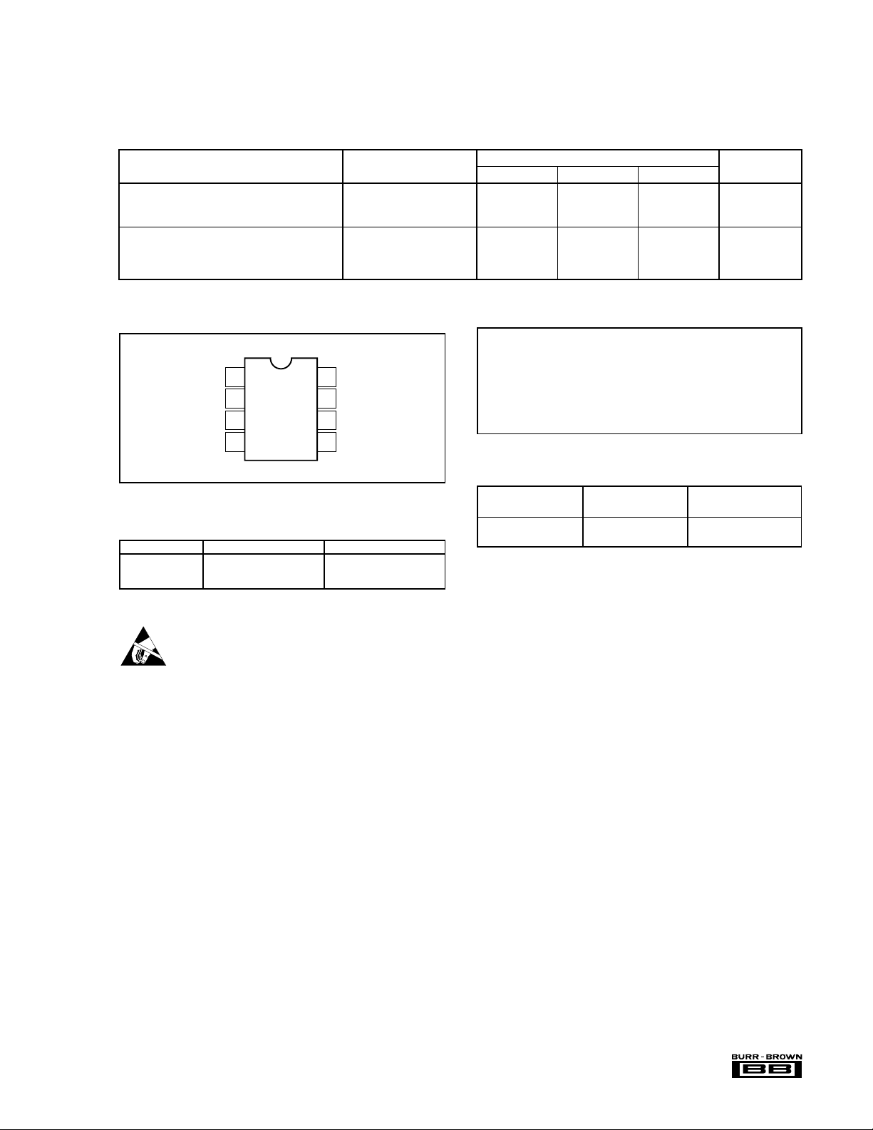
PIN CONFIGURATION ABSOLUTE MAXIMUM RATINGS
Top View DIP/SO-8
Ground
V
1
A
0
2
A
1
3
4
IN
8
V+
7
V
O
6
V–
5
NC
ORDERING INFORMATION
MODEL PACKAGE TEMPERATURE RANGE
PGA103P 8-Pin Plastic DIP –40°C to +85°C
PGA103U SO-8 Surface-Mount –40°C to +85°C
= 0V ±2.6 ±3.5 mA
IN
Supply Voltage................................................................................. ±18V
Analog Input Voltage Range ..................................................... V– to V+
Logic Input Voltage Range ........................................................ V– to V+
Output Short Circuit (to ground) ............................................ Continuous
Operating Temperature ................................................ –40°C to +125°C
Storage Temperature.................................................... –40°C to +125°C
Junction Temperature ................................................................... +150°C
Lead Temperature (soldering,10s) .............................................. +300°C
PACKAGE INFORMATION
MODEL PACKAGE NUMBER
PGA103P 8-Pin Plastic DIP 006
PGA103U SO-8 Surface-Mount 182
NOTE: (1) For detailed drawing and dimension table, please see end of data
sheet, or Appendix D of Burr-Brown IC Data Book.
PACKAGE DRAWING
(1)
ELECTROSTATIC
DISCHARGE SENSITIVITY
Any integrated circuit can be damaged by ESD. Burr-Brown
recommends that all integrated circuits be handled with appropriate precautions. Failure to observe proper handling and
installation procedures can cause damage.
ESD damage can range from subtle performance degradation
to complete device failure. Precision integrated circuits may
be more susceptible to damage because very small parametric
changes could cause the device not to meet published specifications.
The information provided herein is believed to be reliable; however, BURR-BROWN assumes no responsibility for inaccuracies or omissions. BURR-BROWN assumes
no responsibility for the use of this information, and all use of such information shall be entirely at the user’s own risk. Prices and specifications are subject to change
without notice. No patent rights or licenses to any of the circuits described herein are implied or granted to any third party. BURR-BROWN does not authorize or warrant
any BURR-BROWN product for use in life support devices and/or systems.
3
PGA103
Page 4

DICE INFORMATION
6
NC
7
8
NC NC
NC
NC
4C
PAD FUNCTION
1A
2A
3A, 3B, 3C
4A, 4B, 4C
NC: No Connection
NOTES: (1) Connect all three indicated pads. (2) Connect
all three indicated pads.
Substrate Bias: Internally connected to V– power supply.
(1)
(2)
6V–
7V
8V+
0
1
Ground
V
IN
O
1
2
4B4A3C3B3A
PGA103 DIE TOPOGRAPHY
TYPICAL PERFORMANCE CURVES
TA = +25°C, VS = ±15V unless otherwise noted.
MECHANICAL INFORMATION
MILS (0.001") MILLIMETERS
Die Size 69 x 105 ±5 1.75 x 2.67 ±0.13
Die Thickness 20 ±3 0.51 ±0.08
Min. Pad Size 4 x 4 0.1 x 0.1
Backing Gold
50
40
30
20
10
Voltage Gain (dB)
0
–10
10k 100k 1M 10M
VOLTAGE GAIN vs FREQUENCY
G=100
G=10
G=1
Frequency (Hz)
®
PGA103
120
100
80
60
40
20
Power Supply Rejection (dB)
0
10 100 1k 10k 100k 1M
4
POWER SUPPLY REJECTION vs FREQUENCY
G=100
G=10
G=1
Frequency (Hz)
Page 5

®
TYPICAL PERFORMANCE CURVES (CONT)
INPUT CURRENT NOISE vs FREQUENCY
10
1
0.1
1 10 100 1k 10k 100k 1M
Frequency (Hz)
All Gains
100
TA = +25°C, VS = ±15V unless otherwise noted.
1000
100
10
Voltage Noise (nV/√Hz)
1
4
3
2
INPUT VOLTAGE NOISE vs FREQUENCY
G=10
G=100
Bandwidth
Limited
1 10 100 1k 10k 100k 1M
Frequency (Hz)
QUIESCENT CURRENT vs TEMPERATURE
G=1
Current Noise (pA/√Hz)
SMALL SIGNAL RESPONSE
G=1
G=10 G=100
50mV/div
1
Quiescent Current (mA)
0
–50 –25 0 25 50 75 100 125
Temperature (°C)
LARGE SIGNAL RESPONSE
2µs/div
G=10
G=1
5V/div
G=100
2µs/div
5
PGA103
Page 6

APPLICATION INFORMATION
Figure 1 shows the basic connections required for operation
of the PGA103. Applications with noisy or high impedance
power supplies may require decoupling capacitors close to
the device pins as shown.
V+
V–
+15V
8
PGA103
A
1
2
–15V
A
6
7
3
0
1
VO = G • V
IN
0.1µF 0.1µF
V
IN
4
Some applications select gain of the PGA103 with switches
or jumpers. Figure 2 shows pull-up resistors connected to
assure a noise-free logic “1” when the switch or jumper is
off or open. Fixed-gain applications can connect the logic
inputs directly to V+ or ground (or other valid logic level)
without a series resistor.
V+ V–
8
6
74
V
A
0
3
1
1
2
S
0
O
GAIN S1S
1 Closed Closed
10 Closed Open
100 Open Closed
Not Valid Open Open
0
V+
V
IN
100kΩ
100kΩ
PGA103
A
S
1
GAIN A1A
1
10
100
Not Valid
NOTE: (1) Low impedance ground connection required for good gain
accuracy—see text.
0
0
0
0
1
1
1
Logic 0: (–5.6) ≤ V ≤ 0.8V
0
Logic 1: 2V ≤ V ≤ (V+)
1
Logic voltages referred to pin 3.
FIGURE 1. Basic Connections.
The input and output are referred to the ground terminal,
pin 3. This must be a low-impedance connection to assure
good gain accuracy. A resistance of 0.1Ω in series with the
ground pin will cause the gain in G=100 to decrease by
approximately 0.2%.
DIGITAL INPUTS
The digital inputs, A
and A1, select the gain according to
0
the logic table in Figure 1. The digital inputs interface
directly to common CMOS and TTL logic components. The
logic inputs are referenced to the ground terminal, pin 3.
The logic table in Figure 1 shows that logic “1” on both A
and A1 is invalid. This logic code will not cause damage, but
the amplifier output will not be predictable while this code
is selected. The output will recover when a valid code is
selected.
The digital inputs are not latched, so a change in logic inputs
immediately selects a new gain. Switching time of the logic
is approximately 0.5µs. The time to respond to gain change
is equal to the switching time plus the time it takes the
amplifier to settle to a new output voltage in the newly
selected gain (see settling time specifications).
Many applications use an external logic latch to access gain
control signals from a high speed data bus. Using an external
latch isolates the high speed digital bus from sensitive
analog circuitry. Locate the latch circuitry as far as practical
from analog circuitry to avoid coupling digital noise into the
analog circuitry.
®
PGA103
FIGURE 2. Switch or Jumper-Selected Gains.
OFFSET TRIMMING
Offset voltage is laser-trimmed to typically less than 200µV
(referred to input) in all three gains. The input-referred offset
voltage can be different for each gain.
+15V –15V
V
IN
0
NOTE: (1) Op amp buffer is required to preserve good gain accuracy—see
text.
PGA103
A
0
A
1
1
2
Trim Range
Logic threshold voltage
is altered by V
OK for V
≤ 100mV.
TRIM
3
V
(1)
TRIM
TRIM
±5mV
OPA602
.
VO = G (VIN – V
100kΩ
33Ω
TRIM
)
FIGURE 3. Offset Voltage Trim Circuit.
Figure 3 shows a circuit used to trim the offset voltage of the
PGA103. An op amp buffers the trim voltage to provide a
low impedance at the ground terminal. This is required to
maintain accurate gain. Remember that the logic inputs, A
and A1, are referenced to this ground connection, so the
logic threshold voltage will be affected by the trim voltage.
This is insignificant if the offset adjustment is used only to
trim offset voltage. If a large offset is used (greater than
0.1V), be sure that the logic input signals provide valid logic
levels when referred to the voltage at the ground terminal,
pin 3.
6
+15V
50kΩ
–15V
0
Page 7

®
4
V+V
8
PGA103
A
0
A
1
2
–
= 1, 10, 100
G
2
6
3
1
7
V
O
• G
G = G
1
2
–
V+V
G1 = 1, 2, 4, 8
–
V
IN
PGA205
+
V
IN
True
instrumentation
amplifier input.
GAIN
1
0
0
0
0
0
1
0
0
1
0
0
0
1
1
0
0
0
0
1
0
0
1
1
0
1
0
1
0
1
1
1
0
0
0
0
1
0
1
0
1
1
0
0
1
1
1
0
1
10
20
40
80
100
200
400
800
2
4
8
FIGURE 4. Programmable Gain Instrumentation Amplifier.
+15V
–15V
V
IN
Accepts inputs
to ±120V.
102kΩ
D
1
11.3kΩ
D
2
PGA103
A
1
A
0
G = 0.1, 1, 10
D1, D2; IN4148
A1A
0
FIGURE 5. Wide Input Voltage Range Amplifer.
V
O
MODEL CHARACTERISTICS
INA103 Low Noise, 1nV/√Hz IA
INA105 G = 1 Difference Amp
INA106 G = 10 Difference Amp
INA114 Resistor-Programmed Gain, Precision
+
V
IN
–
V
IN
G
INA
INA117 ±200V C-M Input Range Difference Amp
INA111 FET Input, High Speed IA
INA131 Precision, G = 100 IA
FIGURE 6. Instrumentation Amplifier with Programmable Gain Output Amp.
1
G2 = 1, 10, 100
PGA103
A
A
1
0
V
G = G
O
• G
1
2
7
PGA103
 Loading...