

Page 1

PFCM Design Guide
PFCM Design Guide with Analog PFC IC
HP SPM & System Engineering Group
FAIRCHILD SEMICONDUCTOR
82-3, Dodang-Dong, Wonmi-ku, Puchon, Kyonggi-Do, KOREA
Tel) 82-32-680-1834, Fax) 82-32-680-1823
Feb. 2006 FAIRCHILD SEMICONDUCTOR – System Engineering Group
1
Page 2

PFCM Design Guide
Contents
1. System Configurations.......................................................................... 3
2. Protection Circuits................................................................................. 3
Over Current Protection (OCP).............................................................................................................. 3
Over Voltage Protection......................................................................................................................... 4
Under Voltage Protection....................................................................................................................... 4
3. Design Example (PFCM DEMO BOARD).............................................. 5
Operating conditions of PFCM demo board:........................................................................................... 5
Output capacitance and Inductance design............................................................................................ 5
Output Voltage Ripple & Output Capacitance. .....................................................................................5
Inductance & Input Current Ripple ........................................................... ......... ..... .... ..... ......... ............ 6
Open Loop Response................................................................................................................................ 6
Current Loop Amplifier................................................... ....................................................................... 7
Voltage Loop Amplifier .......................................................................................................................... 7
Control Loop Implementation................................................................................................................ 8
Current Loop................................................. ....................................................... ................................... 8
Voltage Loop........................................................................................................................................... 9
Other Parameters................................ ....................................................... .......................................... 10
Over Current Protection....................................................................................................................... 12
Over Voltage Protection....................................................................................................................... 13
DC-link Voltage Control........................................................................................................................... 14
4. Experimental Results........................................................................... 15
Feb. 2006 FAIRCHILD SEMICONDUCTOR – System Engineering Group
2
Page 3
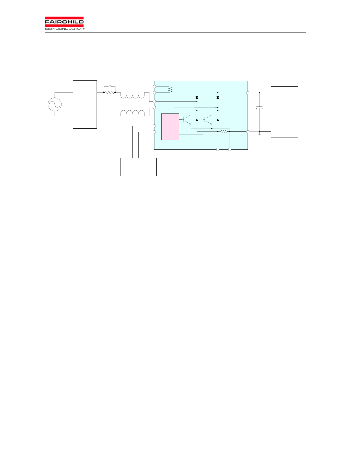
1. System Configurations
PFCM Design Guide
V
ac
Relay
N/ F
V
TH
R
TH
S
R
NTC
Thermistor
P
R
SPM
IN
(S)
LVIC
IN
(R)
Shunt
Resistor
V
AC-
N
N
SENSE
Control IC
Fig.1 Typical block diagram of PFCM system
An inrush-current prevention circuit is required due to the large DC link capacitance as shown in Fig. 1.
The relay of the circuit should be closed after DC link capacitor is charged far enough. PFCM, mini-SPM and
control IC can share single GND stage. Usually, this GND and the N
terminal of PFCM should have the
SENSE
same potential. Large surge voltage is easily produced between P and N terminals by large current switching.
To reduce surge voltage it is important to shorten the DC link bus wiring between PFCM and DC link
capacitor. In addition, good high frequency characteristic capacitor, such as polypropylene film capacitor
should be mounted near to P and N terminals as a snubber.
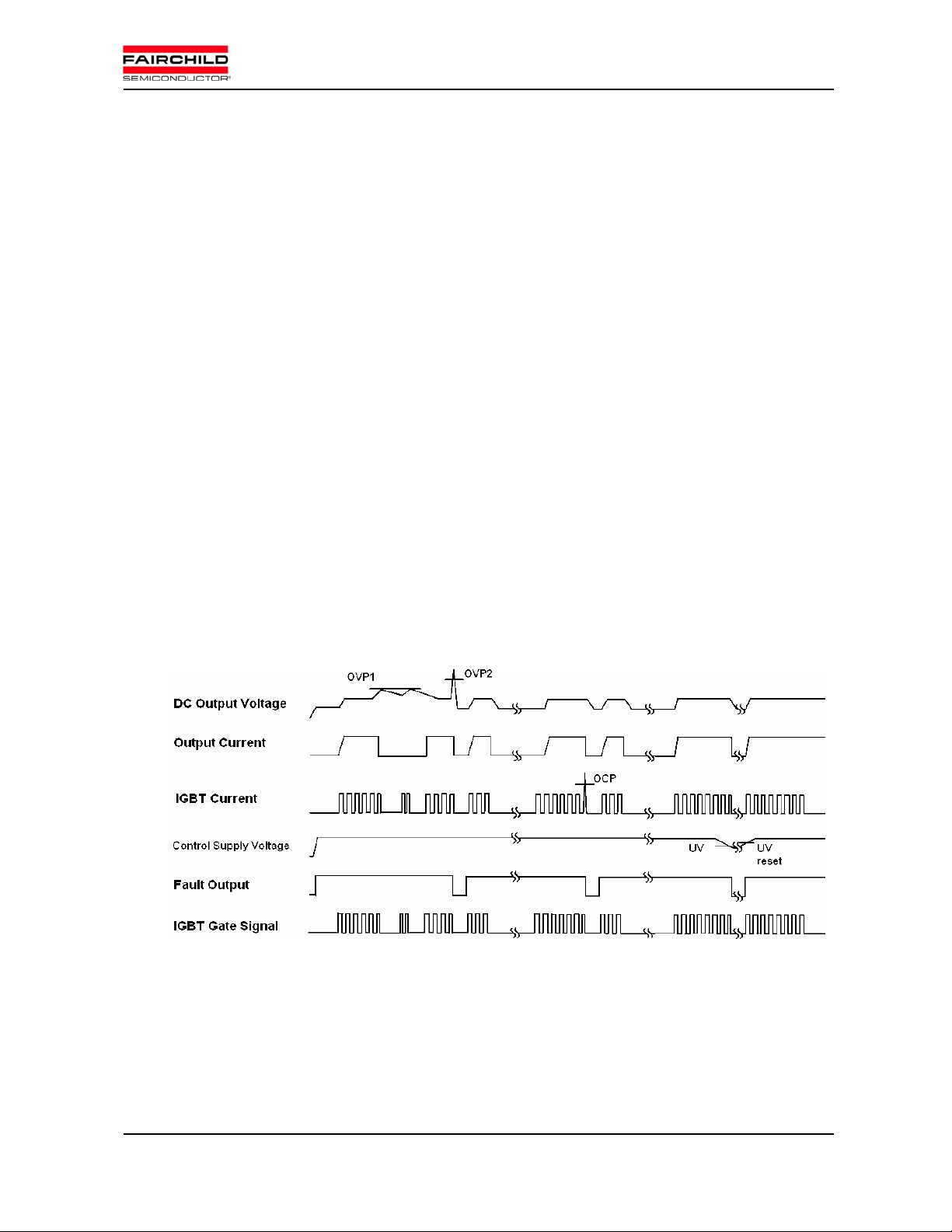
2. Protection Circuits
Following Fig. 2 shows the timing chart of protection function. There are two kind of protection level for
both OCP and OVP. Generally, PFC control ICs have its own OCP and OVP function. Also, user can make
the PFCM stop and output the FO signal under preset OC, OV condition using its Csc input.
Over Current Protection (OCP)
[OCP Level1 –P FCM ] PFCM can protect from over current situation. When OC(over current) situation
happens, the PFCM stops operating and generates fault out signal during fault-out duration time(set by C
And then after the duration, it works again according to the input command. Its total propagation delay time
may depend on outer op-amp speed. We recommend using a low cost slow op-amp solution with fast
protection. It is the OCP level2 protection described in next paragraph.
[OCP Level2 (SCP) –PFC control IC] By the peak current limit function of PFC control IC, the system
is protected from SC(Short Circuit) situation. The recommended current limit of OCP level 2 is higher than
FOD
).
Feb. 2006 FAIRCHILD SEMICONDUCTOR – System Engineering Group
3
Page 4
PFCM Design Guide
that of OCP level 1. It doesn’t generate the fault out signal but its response is very fast. It will protect the
system from short circuit situation during the propagation delay time of OCP level1.
Over Voltage Protection
OV (Over Voltage) protection can be also implemented by dual protection. The DC-link voltage
changes slowly because of its large capacitance. So OVP does not need fast response. Therefore it is
optional to activate the OVP of PFC controller.
[OVP Level 1 - PFC co ntroller] OVP level 1 suppresses voltage overshoot in transient situation. It
doesn’t generate fault out signal.
[OVP Level 2 – PFCM] The voltage level of OVP level 2 is higher than that of OVP level 1. When OV
situation happens, the PFCM stops operating and generates fault out signal during fault-out duration time(set
by C
Under Voltage Protection
). And then it works again.
FOD
IGBT gate will be interrupted when control voltage drops below UV trip level, and the protection will be realeased
automatically if the control voltage recovers to the UV reset level.
Fig.2 Timing chart of protection function
Feb. 2006 FAIRCHILD SEMICONDUCTOR – System Engineering Group
4
Page 5
PFCM Design Guide
3. Design Exa mple (PFCM DEMO BOARD)
A general PFC example is implemented for 5[kW] air-conditioning applications whose input voltage is
187~276[V].
Operating conditions of PFCM demo board:
Table 1. The operating conditions.
Item Symbol Value Unit
1 Switching Frequency Fsw 40 KHz
2 Minimum Input Voltage Vimin 176 Vac
3 Nominal Input Voltage Vinom 220 Vac
4 Maximum Input Voltage Vimax 264 Vac
5 Output Max. Power Po 5000 W
6 Minimum Output Voltage Vom in 350 Vdc
7 Nominal Output Voltage Vonom 380 Vdc
8 OVP level 1 V
9 OVP level 2 V
420 V
OV1
440 V
OV2
10 Peak Ripple Current Iripple 5 A
11 OCP Level1 Iocp1 40 A
12 OCP Level2 (SCP) Iocp2 50 A
13 Shunt Resistor Rsh 2 MOhm
14 DC Capacitor Cout 940 uF
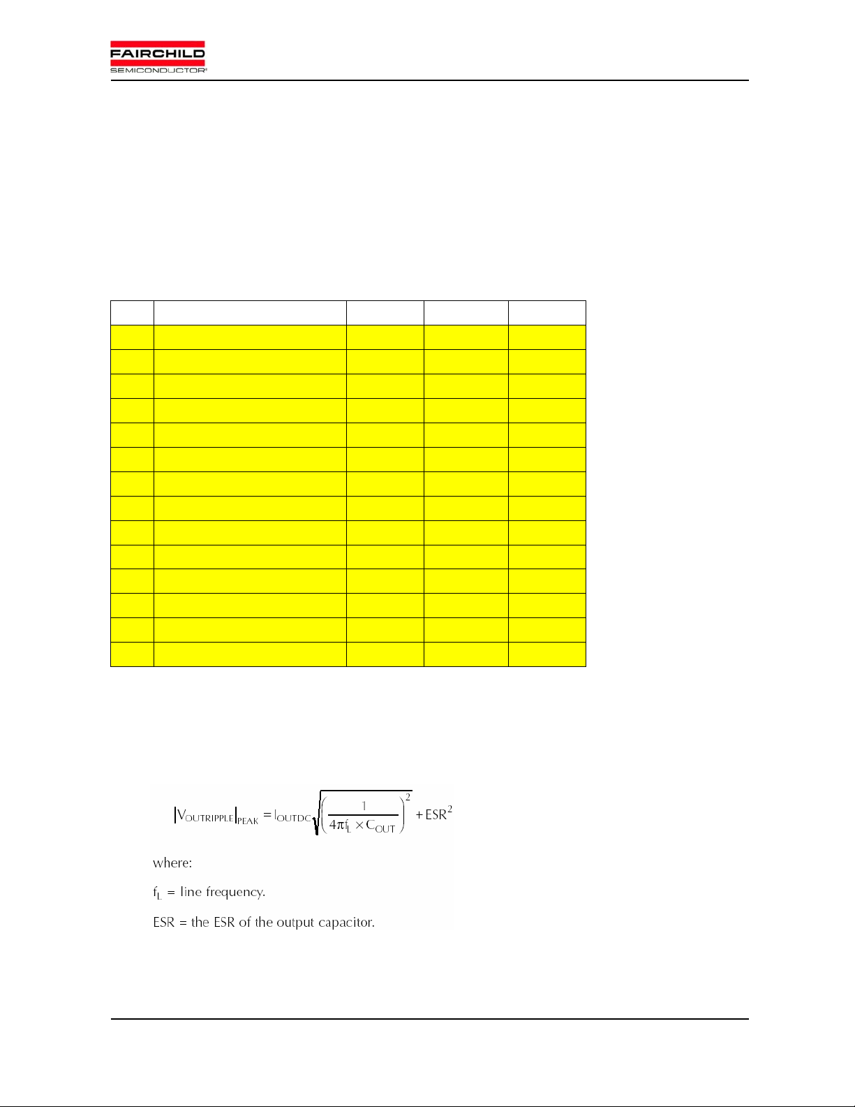
Output capacitance and Inductance design
Output Voltage Ripple & Output Capacitance
Voltage ripple of V
(470[uF] x 2)
Feb. 2006 FAIRCHILD SEMICONDUCTOR – System Engineering Group
can be reduced by employing large C
DC
5
. In demo board, C
OUT
is set to 940[uF]
OUT
Page 6
Inductance & Input Current Ripple
∴
where: ΔI
V
V
: Peak to peak current of PFC inductor
Lp-p
: Input AC voltage
IN
: DC link Voltage
OUTDC
f : Switching frequency
L : Inductance of PFC inductor
VVV
OUTDC
fL
4
INOUTDCIN
(
=Δ
I
L
PP
−
I
fLV
OUTDC
)( =Δ
PP
−
V
MAXL
PFCM Design Guide
)( −
1
VV
=∵
2
)
OUTDCIN
V
OUTDC
L
Î
AI
5)( =Δ
MAXL
PP
−
20Hf
380
==
4000020
⋅
=
][475
μ
(fs=40kHz)
Current ripple is decided by switching frequency and inductance. To reduce current ripple, high
switching frequency and large inductance value is required. It means that employing higher switching
frequency can reduce inductor size. But the power losses will increase and it requires more efficient heat
sink structure.
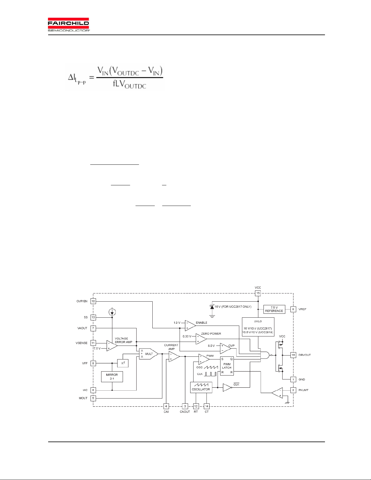
Open Loop Response
Fig.3 Block diagram of PFC control IC
Feb. 2006 FAIRCHILD SEMICONDUCTOR – System Engineering Group
6
Page 7

PFCM Design Guide
The following is the block diagram of PFC controller ucc3818. The average current mode control is
composed of two types of loops- voltage loop and current loop. The voltage loop controls the output DC-Link
voltage. It regulates the output voltage. There is a 120[Hz] ripple voltage in the output DC-Link, which is
caused by the 60[Hz] ac input current. Hence, the voltage loop must be designed to be slow enough to reject
the 120[Hz] ripple voltage.
In general CCM (Continuous Current Mode) PFC IC, there is a multiplier. It multiplies V
voltage loop) by I
voltage). The output(
The difference between the voltage of I
sensing resister is amplified by the current loop. The V
(reference of input ac current shape) and then divides it by V
AC
IVKI⋅
ACEA
MO
⋅=
V
) of a multiplier is the reference of the PFC’s input current(IAC).
2
RMS
pin(output of the multiplier) and the voltage of the current
MO
(output of the current loop) is the reference voltage
EA
(reference of rms input
RMS
to the comparameter that generates the gating signal. Current loop should be fast enough to catch up with
the 120[Hz] input ac current. But too fast speed can distort the current shape due to the switching noise.
Therefore, the current loop must be designed to be fast enough to catch up with the 120[Hz] rectified input
current, but not too fast for switching noise immunity.
(the output of
EA
Current Loop Amplifier
Eq. 1 shows the open loop response of power stage. (Refer to UCC3818 datasheet)
G
PST
S
IAOUT
where: V
V
V
R
sV
)(
sV
: Voltage of shunt resistor
S
: Voltage of RMO
IAOUT
: DC link Voltage
DC
: Shunt resistance for current sensing (2mohm)
SH
RV
== (UCC3818) (Eq.1)
SHDC
sL
4)(
L : PFC inductance
s : jω(= j⋅2πf)
Voltage Loop Amplifier
Eq. 2 shows the open loop response of power stage. (Refer to UCC3818 datasheet)
P
G
=
LOV
...
where: P
C
V
ΔV
IN
OUT
OUTDC
IN
Δ
VVsC
(UCC3818) (Eq.2)
EAOUTOUTDCOUT
: Input power
: DC link capacitance
: DC link voltage
: Error amplifier output difference (≈5V)
EAOUT
s : jω(= j⋅2πf)
Feb. 2006 FAIRCHILD SEMICONDUCTOR – System Engineering Group
7
Page 8

PFCM Design Guide
Control Loop Implementation
Current Loop
[Step 1] Crossover frequency
Theoretical crossover frequency is given by following equation.
f
S
f
C
[Step 2] Fz and Fp decision
f
C
f
Z
[Step 3] Rz, Cp, Cz decision
is same to RMO. (Refer to “other parameters” in page 10)
R
i
R
= 470[Ω],
i
In Eq.1,
G
Therefore it requires 40dB boosting at fc(=6.6kHz).
kHz
7.66⇒= (Eq.3)
3.32==
kHz
=
C
6.6
, kHzff
kHzfPST
RV
sL
ZP
206==
π
RV
SHDCSHDC
Lf
)2(44
C
dB
8.390103.0
−====
R
is given by Eq.7.
z
R
z
G
dB
R
40log20 == Æ R
i
dB
= 47[kΩ],
z
From Eq.4 ,Eq.5, Cp and Cz is given.
= 180[pF], Cz = 1[nF]
C
p
1
f
=
z
π
2
f
=
p
π
2
(Eq.4)
CR
zz
CC
+
pz
(Eq.5)
CCR
pzz
R
i
R
IA
IA
MO
R
z
C
CA
z
OUT
C
p
-
+
Fig.4 Current loop circuit
Feb. 2006 FAIRCHILD SEMICONDUCTOR – System Engineering Group
8
Page 9

(
=
FZ=3.3kHz
PFCM Design Guide
FC=6.7kHz
FP=20kHz
Voltage Loop
G
A resistor(R
replaced by small SMD type capacitor.
Æ
Fig.5 Desired current error amplifier response
[1]
[2]
[3]
=
LOV
...
VD
f
CV
G
dB
G
dB
G
dB
P
IN
) is added between E/A input and sensing resistor. By virtue of large RVD, CVF can be
VD
Ω= kR
120 (>R
VDVF
1
π
2
log20=
log20= (Eq.7)
log20=
Δ
EAOUTOUTDCOUT
VS
Ω≈⋅= MRR
18
<<=
CR
VFVD
π
2
R
z
R
i
π
2
=
)
(>RVD)
120
Æ CVF=1uF
1
(Eq.6)
CfR
zi
1
(Eq.8)
CfR
pi
5000
π
CV
=
5380001.02
⋅⋅⋅
419
ffVVsC
3.1
)
Hzf
Feb. 2006 FAIRCHILD SEMICONDUCTOR – System Engineering Group
9
Page 10

Other Parameters
RT, CT: Switching frequency decision
f
=
R
= 15[kΩ]
T
C
= 1[nF]
T
Î F
R
: (Refer to fig.4)
MO
6.0
CR
TT
= 40[kHz]
s
Vdc
R
VL
R
VD
R
VS
Fig.6 Voltage loop circuit
PFCM Design Guide
R
VF
C
VF
EA
-
V
ref
EA
OUT
⋅
RI
MO
I
_
=
R
GMMAX
sensepeakAC
=
(Assuming the input current is 50A
= 470[Ω]
Î R
MO
= 0.002[Ω]( small resistance can cause distortions at low level current)
R
sense
R
& Optocoupler circuit:
AC
002.0250
⋅
6
−
10300
×
@ VAC = 100V
RMS
RMS
][470471
Ω≈=
)
Optocuopler: TLP180
Feb. 2006 FAIRCHILD SEMICONDUCTOR – System Engineering Group
10
Page 11

PFCM Design Guide
=×Ω
RAX
VCC
1
4
Optocoupler
2
3
RL
CL
RAC
Rc1
Rc2
-
+
Fig.7 Input AC voltage sensing circuit
RFF
ISIN
E
VFF
UCC3818
CFF
R
and RL depend on optocoupler :
AX
⋅
V
RMS
=
R
AX
I
LINEAR
Æ
2
max_
=
max_
2270
⋅
3
−
106
×
+++
][64
Ω=
k
)245.0]([18181818 Wk
V
PEAKRL
V
FF
R
AC
R
L
, RC2 , CL, and an op-ampÆ I
R
C1
= 1[uF], RC1 = 0[Ω], RC2 = 150[Ω],
C
L
:
R
= 33[kΩ], CFF = 100[uF]
FF
Feb. 2006 FAIRCHILD SEMICONDUCTOR – System Engineering Group
_
I
AC
max_
][390 Ω=
][4.1 VVFF= (when, input voltage V
9
==
3
−
105.0
×
SINE
AC
][18
Ω=
k
off-set compensation
= 90[VAC])
11
Page 12

Over Current Protection
∴
∴
PFCM Design Guide
OCP
+
OUT
PFCM
R
19
R
40
R
VAC-
18
Fig.8 Over current protection circuit
R
37
R
38
VREF(7.5V)
PKLIMIT
UCC3818
The actual protection level can be slightly different from the calculated value. It depends on PCB
layout pattern. About demo board, the designed values are:
R
= R40 = 1.2[kΩ], R19 = R37 = 82[kΩ], R38 = 1.5[kΩ]
18
And the expected OC levels are:
1) OCP level 1
)(
R
38
R
37
=
V
REF
][40 AIPK≈
−+
++
RRR
RIRVRR
194018
PKSHREF
I
PK
⎛
V
REF
⎜
⎜
RR
19401918
SH
⎝
R
38
RR
4018
()
R
37
⎞
⎟
++−+=⇒
RRR
401918
⎟
⎠
2) OCP level 2
RR
+
R
18
V
4019
REF
IR
][50 AIPK≈
I
=⇒=
PKSH
PK
VR
18
REF
()
SH
+
RRR
4019
Feb. 2006 FAIRCHILD SEMICONDUCTOR – System Engineering Group
12
Page 13

Over Voltage Protection
About demo board, the designed values are:
PFCM Design Guide
Vdc
R
Z
OVP1
R
Y
OVP2
R
X
Fig.9 Over voltage protection circuit
= 15 [kΩ], RY = 1.8 [kΩ], RZ = 870 (270+270+330) [kΩ]
R
X
And the expected OC levels are:
1) OVP level 1
RR
+
YX
++
2) OVP level 2
R
X
++
V
_
OVREF
RRR
ZYX
RRR
ZYX
_
PKDC
V
REF
V
_
V
PKDC
V
V
=⇒=
PKDC
=⇒=
PKDC
_
++
RR
+
++
R
X
RRR
ZYX
__
REF
OVREF
15
YX
RRR
ZYX
8.886
=⋅=
][4228
VV
8.16
8.886
=⋅=
][4435.7
VV
Feb. 2006 FAIRCHILD SEMICONDUCTOR – System Engineering Group
13
Page 14

DC-link Voltage Control
Vdc
R
VL
PFCM Design Guide
R
VF
C
VF
R
VD
EA
-
V
R
VS1
R
VS2
OP-AMP
Fig.10 DC link voltage control circuit
ref
Outer
EA
OUT
R
D1
D2
R
The relation between V
⎛
⎛
⎜
5.7
⎜
⎝
R
⎜
RV
VLDC
⎜
⎝
and parameters is:
DC
VD
⎞
11
⎟
++=
⎟
RRRR
VSVFVSVF
⎠
⎞
R
VD
⎟
1
++
⎟
⎠
⎛
1
⎜
⎜
RR
VFVF
⎝
RR
++−
VLVD
The variable V
voltage is available by just changing V
DC
voltage. VEA, the output of voltage error
SIG
amplifier changes from 0 to 5.5V as its load current. In no load condition, V
voltage of V
will be the highest value. The next graph shows V
DC
and VDC voltage. The voltage of VDC in
SIG
low load condition is higher than that of max. load condition.
V
SIG
⎞
RR
VDVL
⎟
V
EA
⎟
R
VS
⎠
value is almost zero. And the
EA
⎛
R
VL
−
R
VS
R
D
⎜
⎜
1111
⎝
1
RR
+
DD
21
⎞
⎟
V
SIG
⎟
⎠
[V]
V
DC
Min. load
Max. load
V
[V]
SIG
Fig.11. DC link voltage vs. control voltage
Feb. 2006 FAIRCHILD SEMICONDUCTOR – System Engineering Group
14
Page 15

PFCM Design Guide
4. Experimental Results
Fig. 12 shows the overall schematics of implemented PFC converter. Table 2 shows the components
that are used for the implemented hardware. Fig. 13 shows the input ac current and DC-link voltage
waveforms. These figures’ details are shown in table 3.
HEADER 7
OVP1
VCC
12
Vin
TP
1
R13
10
1 2
PWIN
CNT2
1
2
3
4
5
6
7
R46
0
1 2
VREF
Vfo
TP
VCC
1
ENA
-FAULT
VSIG
VCC
U8A
411
OVP
R32
1
TP
20K
3
+
1 2
1
2
-
KA224
C30
C31
101
AC1
VTR-250
AC2
VTR-250
104
1
2
1
2
143
D5
DF08S
VREF
C34
104
12
RV1
SVC471D
R4
1 2
18K 3216
-+
R49
2
1 2
18K 3216
1 2
1 2
+
C8
33uF/35V
C10
101
C11
PCFN-112
PCFN-112
R34
20K
1 2
C35
101
K1
K2
333
C13
101
VCC
C27
104
U8B
411
5
+
7
6
-
KA224
3
3
J1
VTR-250
t
2
J5
VTR-250
VCC
12
54
ISO1
TLP181
12
R5
390
R48
C15
150
105
C14
104
R37
82K
PKLIMIT
R38
1.5K
2
1
4
2
1
4
RT1
NTC
1 2
F1
220V/30A
112
R51
1 2
18K 3216
R50
1 2
18K 3216
TP2
1
TP
Fig.12. Schematic diagram of the implemented PFC converter.
NOTE:
1. C8 and C9 should be close as possible!
U4
C9
104
1
Vcc
2
COM(L)
3
NC
4
IN(R)
5
IN(S)
6
VFO
7
CFOD
8
CSC
9
NC
10
Csc
NC
TP
11
1
NC
12
NC
13
NC
14
NC
R31
15
20K
NC
16
NC
1 2
17
NC
18
NC
19
RTH
20
VTH
SPM27-GA
1 Ipk
TP
U7
7812
12V
3
C44
105
D1
US1J
RY
1
R23 10K
TP
123Q1
BSS133
R24
10K
J6
VTR-250
1
2
1
2
R53
1 2
C2
224/275V
470K 5025
R3
1 2
470K 5025
1
2
1
2
J2
VTR-250
Vac
1
TP
Offset
1
TP
14
NR/VAC-
IN1COM2OUT
NSENSE
P
VTR-250
1
27
PR
26
S
25
R
24
N
23
NC
22
21
VCC
R52
1 2
470K 3216
12
R1
470K 3216
R2
C1
47K
105
U8D
KA224
-
13
+
12
4 11
VCC
DCP
C12
224/630V
DCN
N
VTR-250
1
2
1 2
1 2
R20
470
1 2
CAO
TP
1
2
R55
270K 3216 F
1 2
VAO
1
TP
12
R9
15K 2012 F
R29
1 2
U5
UC3818
GND
DRVOUT
PKLMT
CAOUT
CAI
MOUT
IAC
VAOUT
VFF8VREF
1
VREF
JP1
FAN
1
2
3
12
R6
270K 3216 F
R44
270K 3216 F
1 2
JP2
8
C38
JUMPER
104
16
PWIN
15
VCC
14
13
12
11
10
9
R25
15K
1 2
C26
101
C19
105
Title
<Title>
Size Document Number Rev
<Doc> <RevCode>
C
Date: Sheet
3.9K 2012 F
VSENSE
OVP/EN
Vref
TP
1 2
VCC
CT
SS
RT
U8C
KA224
-
9
+
10
R28 1M
4 11
1 2
VSIG
C29
R30
VCC
104
1M
1 2
C17
102
VCC
C24
105
C21
104
VCC
10K
R41
123Q2
1 2
D12
Zener 5.6V
R8
4.7k
ENA
C37
104
1
PFC SW
SW SPDT - 1
2
3
GND
Vcc
1
1
TP
TP
VCC
of
11Thursday, September 08, 2005
KRC102
D8
VCC
LED
12
R7
270K 3216 F
C5
470uF/450V
R47
56
C40
183
C25
105
330K 3216 F
12
R45
270K 3216 F
R54
OVP1
1 2
1
TP
OVP1
12
R10
1.8k 2012 F
OVP2
1
TP
OVP2
12
R43
15K 2012 F
VREF
R19
82K
1 2
PKLIMIT
R40
1.2K
1 2
1
2
3
4
5
6
7
12
+
R26
C23
33K
33uF/25V
1 2
1
Vff
TP
12
12
+
C4
+
470uF/450V
TP5
1
TP
R21
470
C39
821
1 2
R18
1.2K
C36
152
R17
C16
47K
181
1 2
C18
102
Iac
TP
1
R22 18K
1 2
R42
R27
120K
1M
1 2
1 2
FAN SUPLY
12V
R11 0
12V
12V
1
TP
Feb. 2006 FAIRCHILD SEMICONDUCTOR – System Engineering Group
15
Page 16

PFCM Design Guide
Table 2. BOM of PFCM demo board.
Item Part Reference Quantity
1 C-Ceramic : 101 2012 C10,C13,C26,C30,C35 5
2 C-Ceramic : 102 2012 C17,C18 2
3 C-Ceramic : 104 2012 SC2,SC4,C9,C14,C21,C27,C29,C31,C34,C37,C38 11
4 C-Ceramic : 105 2012 C1,C15,C19,C24,C25,C44,SC6 7
5 C-Ceramic : 152 2012 C36 1
6 C-Ceramic : 183 2012 C40 1
7 C-Ceramic : 221 2012 C16 1
8 C-Ceramic : 333 2012 C11,SC7 2
9 C-Ceramic : 821 2012 C39 1
10 C-Elec : 220uF 35V SC5 1
11 C-ELEC : 33uF 35V C8,C23 2
12 C-ELEC : 470uF 450V C4,C5 2
13 C-Elec : 47uF 35V SC3 1
14 C-FILM : 105 630V C12 1
15 C-FILM : 220nF AC275V C2 1
16 Connector : 7-pin, 2.54mm pitch CNT2 1
17 DIODE : US1J D1,SD2,SD3,SD4 4
18 FAN connector : 3-pin, 2.54mm pitch JP1 1
19 FPS : KA5M02659RN U10 1
20 Fuse : 220V/20A F1 1
21 JUMPER : 2-pin, 2.54mm pitch JP2 1
22 LED D8 1
23 Main Relay : PCFN-112 K1,K2 2
24 Mosfet : BSS138 Q1 1
25 NTC : 6D-22 RT1 1
26 Op-Amp : KA224 U8 1
27 Opto-coupler : TLP180 ISO1 1
28 Opto-coupler : TLP181 ISO2 1
29 PFC IC : UC3818 U5 1
30 PFCM : FPDB30PH60 U4 1
31 R-Chip : 0ohm, 1/8W, J, 2012 R11,R46 2
32 R-Chip : 1.2Kohm, 1/8W, J, 2012 R40,R18 2
33 R-Chip : 1.5Kohm, 1/8W, J, 2012 R38 1
34 R-Chip : 1.8kohm, 1/8W, F, 2012 SR6,R10 2
35 R-Chip : 1.8kohm, 1/8W, J, 2012 SR2 1
Feb. 2006 FAIRCHILD SEMICONDUCTOR – System Engineering Group
16
Page 17

PFCM Design Guide
36 R-Chip : 100kohm, 1/2W, J, 5025 SR7,SR8 2
37 R-Chip : 10Kohm, 1/8W, J, 2012 SR4,R23,R24,R41 4
38 R-Chip : 10ohm, 1/8W, J, 2012 R13 1
39 R-Chip : 10ohm, 1/8W, J, 2012 SR1 1
40 R-Chip : 120Kohm, 1/8W, J, 2012 R42 1
41 R-Chip : 150ohm, 1/8W, J, 2012 R48 1
42 R-Chip : 15Kohm, 1/8W, J, 2012 R9,R25,R43 3
43 R-Chip : 18Kohm, 1/4W, J, 3216 R4,R49,R50,R51 4
44 R-Chip : 18Kohm, 1/8W, J, 2012 R22 1
45 R-Chip : 1Mohm, 1/8W, J, 2012 R27,R28,R30 3
46 R-Chip : 20Kohm, 1/8W, J, 2012 R31,R32,R34 3
47 R-Chip : 270Kohm, 1/4W, F, 3216 R6,R7,R44,R45,R55 5
48 R-Chip : 3.3kohm, 1/8W, J, 2012 SR3 1
49 R-Chip : 3.9Kohm, 1/8W, J, 2012 R29 1
50 R-Chip : 33Kohm, 1/8W, J, 2012 R26 1
51 R-Chip : 330Kohm, 1/4W, F, 3216 R54 1
52 R-Chip : 390ohm, 1/8W, J, 2012 R5 1
53 R-Chip : 4.7Kohm, 1/8W, J, 2012 R8 1
54 R-Chip : 470Kohm, 1/4W, F, 3216 R1,R3,R52,R53 4
55 R-Chip : 470ohm, 1/8W, J, 2012 R20,R21 2
56 R-Chip : 47Kohm, 1/8W, J, 2012 R2,R17 2
57 R-Chip : 56ohm, 1/8W, J, 2012 R47 1
58 R-Chip : 82Kohm, 1/8W, J, 2012 R19,R37 2
59 R-Chip : 9kohm, 1/8W, F, 2012 SR5 1
60 Regulator : KA78M12 U7 1
61 Switch : SW SPDT - 1 PFC SW 1
62 Terminal : VTR-250 J1,J2,J5,J6,AC1,AC2,P,N 8
63 TR : KRC102 Q2 1
64 Transformer : EI-1916 T1 1
65 TVS : SMBJ170 SD1 1
66 Varistor : SVC471D RV1 1
67 Voltage detector : KA431A SD5 1
68 Zener Diode : 1N4734A, 5.6V D12 1
69 Bridge Diode : DF08S D5 1
Feb. 2006 FAIRCHILD SEMICONDUCTOR – System Engineering Group
17
Page 18

PFCM Design Guide
(50V/div)
V
DC
(10A/div)
I
IN
Fig. 13. Full load test results (I
= 15A
IN
RMS
)
Table 3. Power factor and input power measurement.
V
Fig.13
* VAC and IAC are RMS values
[V] IAC [A]
AC
220 15
Power [kW]
3.3
Power Factor [%]
99
Feb. 2006 FAIRCHILD SEMICONDUCTOR – System Engineering Group
18
 Loading...