

Page 1
PF0121
MOS FET Power Amplifier Module for GSM Mobile Phone
ADE-208-097A (Z)
Application
For GSM CLASS2 890 to 915 MHz
Features
• Low power control current: 0.9 mA Typ
• High speed switching: 1.5 µsec Typ
• Wide power control range: 100 dB Typ
Pin Arrangement
2nd Edition
July 1996
• RF-B2
5
1: Pin
2: V
4
3
2
5
1
APC
3: V
DD
4: Pout
5: GND
Page 2
PF0121
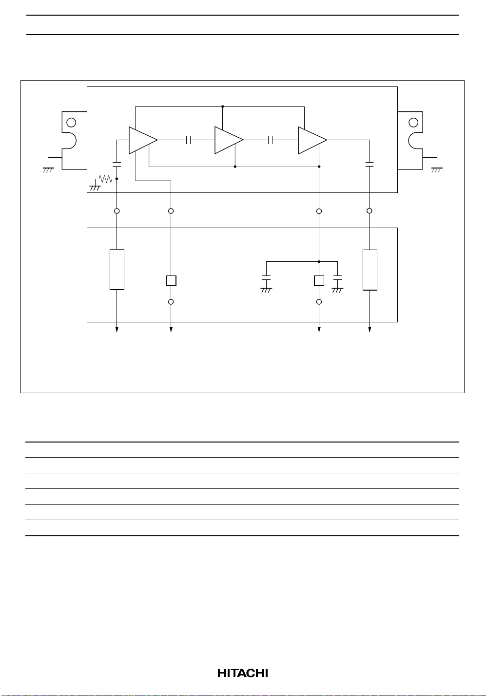
Internal Diagram and External Circuit
G
GND
Pin1
Pin
Z1
Pin
Pin2
V
APC
FB1 FB2
V
APC
C2 C1
Pin3
V
DD
Pin4
Pout
V
DD
Pout
G
GND
Z2
C1 = 0.01 µF (Ceramic chip capacitor)
C2 = 330 µF (Aluminum Electrolyte Capacitor)
FB = Ferrite bead BL01RN1-A62-001 (Manufacture: MURATA) or equivalent
Z1 = Z2 = 50 Ω (Microstrip line)
Absolute Maximum Ratings (Tc = 25°C)
Item Symbol Rating Unit
Supply voltage V
Supply current I
APC voltage V
DD
DD
APC
Input power Pin 20 mW
Operating case temperature Tc (op) –30 to +110 °C
Storage temperature Tstg –40 to +110 °C
17 V
6A
8V
2
Page 3
PF0121
Electrical Characteristics (Tc = 25°C)
Item Symbol Min Typ Max Unit Test Condition
Drain cutoff current I
Total efficiency η
DS
T
— — 500 µAVDD = 17 V, V
30 35 — % Pin = 2 mW, VDD = 12.5 V,
2nd harmonic distortion 2nd H.D. — –50 –40 dBc Pout = 13 W (at APC controlled),
3rd harmonic distortion 3rd H.D. — –55 –45 dBc RL = Rg = 50 Ω, Tc = 25°C
Input VSWR VSWR (in) — 2 3 —
Output power (1) Pout (1) 17 23 — W Pin = 2 mW, VDD = 12.5 V, V
R
=Rg = 50 Ω, Tc = 25°C
L
Output power (2) Pout (2) 9 12 — W Pin = 2 mW, VDD = 10.3V, V
R
= Rg = 50 Ω, Tc = 80°C
L
Isolation — — –60 –40 dBm Pin = 2 mW, VDD = 12.5 V, V
R
= Rg = 50 Ω, Tc = 25°C
L
Switching time tr, t
f
— 1.5 2 µs Pin = 2 mW, VDD = 12.5 V, Pout = 13 W,
R
= Rg = 50 Ω, Tc = 25°C
L
Stability — No parasitic oscillation — Pin = 2 mW, VDD = 12.5 V,
Pout ≤ 13 W (at APC controlled),
Rg = 50 Ω, Tc = 25°C,
Output VSWR = 20:1 All phases
APC
= 0 V
APC
APC
APC
= 7 V,
= 7 V,
= 0.5 V,
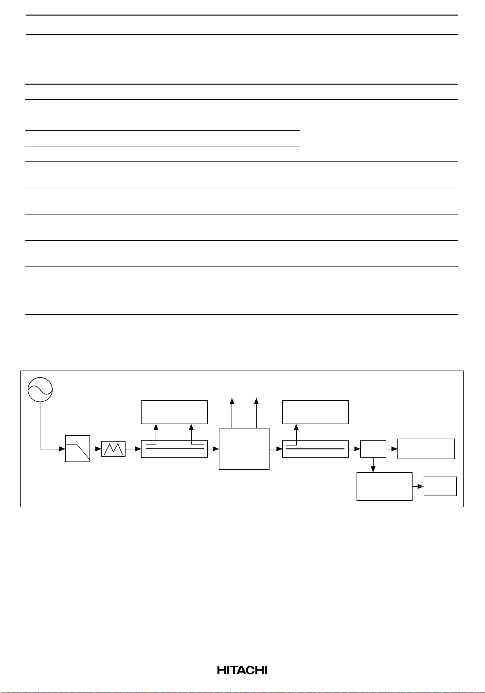
Test System Diagram
S.G
L.P.F
3dB
ATT
Power
Meter
Directional
Coupler
V
APCVDD
Test
Fixture
Spectrum
Analyzer
Directional
Coupler
RF SW.
Phase
Shifter
Power Meter
Short
3
Page 4
PF0121
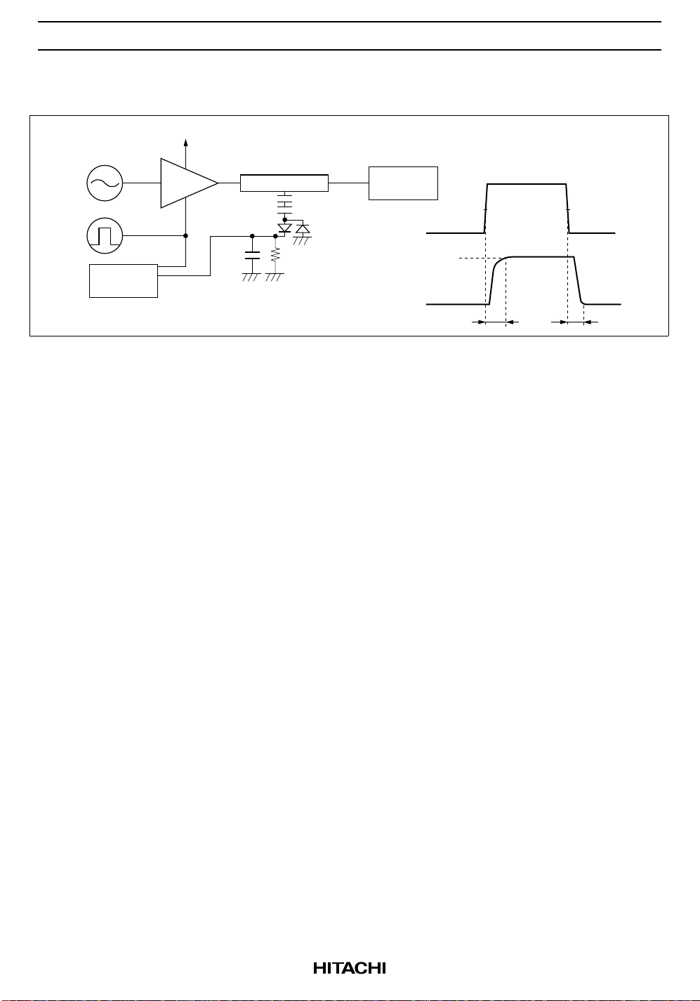
Switching Time Test Diagram
=12.5 V
V
DD
S.G
D.U.T
Pin Pout
P.G
f=10 kHz
Oscillo
Scope
Vout
V
APC
1SS106
Z=50Ω
2.2 kΩ100p
2p
2p
1SS106
Power
Meter
V
APC
Vout
Duty=1/8
50% 50%
95%
5%
tr tf
4
Page 5

Test Fixture Pattern
Unit: mm
PF0121
2.88
15
26.5
3.5
4
4
4.5
2.88
3
V
APC
16
100
2.88
6
V
DD
4
1.5
28
4
80
3.5
2.88
4
16.5
Grass Epoxy Double sided PCB
(t = 1.6 mm, εr = 4.8)
C1=0.01µF (Ceramic Chip Capacitor)
C2=330µF (Aluminum Electrolyte Capacitor)
L1=L2 : BLO2RN1-R62 (Manufacturer : MURATA) or equivalent (Ferrite Bead Inductor)
The coefficient of RF line loss in the P.C.B is showed bellow.
1/ (S
)2 = 1/ (0.9805)2 = 1.068
21
Mechanical Characteristics
Item Conditions Spec
Torque for screw up the heatsink flange M3 Screw Bolts 4 to 6 kg•cm
Warp size of the heatsink flange: S
S
S = 0
+0.3/–0 mm
5
Page 6

PF0121
Note for Use
• Unevenness and distortion at the surface of the heatsink attached module should be less than 0.05 mm.
• It should not be existed any dust between module and heatsink.
• MODULE should be separated from PCB less than 1.5 mm.
Soldering temperature and soldering time should be less than 230°C, 10 sec.
(Soldering position spaced from the root point of the lead frame: 2 mm)
• Recommendation of thermal joint compounds is TYPE G746.
(Manufacturer: Shin-Etsu Chemical, Co., Ltd.)
• To protect devices from electro-static damage, soldering iron, measuring-equipment and human body etc.
should be grounded.
• Torque for screw up the heatsink flange should be 4 to 6 kg · cm with M3 screw bolts.
• Don't solder the flange directly.
• It should make the lead frame as straight as possible.
• The module should be screwed up before lead soldering.
• It should not be given mechanical and thermal stress to lead and flange of the module.
• When the external parts (Isolator, Duplexer, etc.) of the module are changed, the electrical characteristics
should be evaluated enough.
• Don't washing the module except lead pins.
• To get good stability, ground impedance between the module GND flange and PCB GND pattern should
be designed as low as possible.
6
Page 7

Characteristic Curves
6
V
APC
10
f=890 MHz, Pin=2 mW
Pout=13 W, Tc=25
, ηT, VSWR (in) vs. VDD (1)
°
C, Rg=Rl=50 Ω
PF0121
50
5
(V)
4
APC
3
V.S.W.R. (in)
Apc Voltage V
2
1
6
10
5
(V)
4
APC
8
6
4
2
0
10
Supply Voltage V
V
, ηT, VSWR (in) vs. VDD (2)
APC
f=915 MHz, Pin=2 mW
Pout=13 W, Tc=25
8
6
η
T
V
APC
V
SWRin
1211 14
13
°
C, Rg=Rl=50 Ω
η
T
DD
(V)
15
16
40
30
20
10
0
50
40
30
(%)
T
Efficiency η
(%)
T
3
V.S.W.R. (in)
Apc Voltage V
2
1
V
4
APC
20
Efficiency η
2
V
SWRin
0
10
1211 14
13
Supply Voltage V
DD
15
(V)
10
0
16
7
Page 8

PF0121
50
40
(%)
30
T
20
Efficiency η
10
50
40
(%)
30
T
f = 890 MHz
Pin = 2 mW
Tc = 25°C
Rg = Rl = 50Ω
0
0
f = 915 MHz
Pin = 2 mW
Tc = 25°C
Rg = Rl = 50Ω
ηT, Pout vs. V
VDD=12.5 V
η
T
Pout
2
Apc Voltage V
ηT, Pout vs. V
(1)
APC
VDD=15.6 V
15.6 V
4
(V)
APC
(2)
APC
VDD=15.6 V
12.5 V
10.8 V
10.8 V
12.5 V
10.8 V
6
VDD=15.6 V
12.5 V
35
30
25
20
15
10
Output Power Pout (W)
5
0
8
35
30
25
20
10.8 V
15
20
η
T
Efficiency η
10
Output Power Pout (W)
10
Pout
0
0
2
Apc Voltage V
4
APC
6
(V)
5
0
8
8
Page 9

PF0121
, ηT, VSWR (in) vs. Pin (1)
V
APC
6
10
f=890 MHz,
Pout=13 W, Tc=25
VDD=12.5 V,
°
C, Rg=Rl=50 Ω
50
5
(V)
4
APC
3
V.S.W.R. (in)
Apc Voltage V
2
1
6
10
5
(V)
4
APC
8
6
4
2
0
0
26
V
f=915 MHz,
Pout=13 W, Tc=25
8
6
η
T
V
APC
V
SWRin
48
Input Power Pin (mW)
, ηT, VSWR (in) vs. Pin (2)
APC
VDD=12.5 V,
°
C, Rg=Rl=50 Ω
η
T
10
40
30
20
10
0
50
40
30
(%)
T
Efficiency η
(%)
T
3
V.S.W.R. (in)
Apc Voltage V
2
1
4
20
Efficiency η
V
APC
2
V
SWRin
0
0
26
48
10
0
10
Input Power Pin (mW)
9
Page 10

PF0121
, ηT, VSWR (in) vs. Frequency
V
APC
6
10
Pin=2 mW,
Pout=13 W, Tc=25
VDD=12.5 V,
°
C, Rg=Rl=50 Ω
50
5
(V)
4
APC
3
V.S.W.R. (in)
Apc Voltage V
2
1
8
6
4
2
0
890
η
T
V
APC
V
SWRin
895 905
900 910
Frequency f (MHz)
915
40
30
20
10
0
(%)
T
Efficiency η
10
Page 11

Package Dimensions
12.7 ± 0.5
11.0 ± 0.3
+ 0.6
– 0.3
5.0
2.3
13.0 ± 1
60.5 ± 0.5
57.5 ± 0.5
R1.6
2134
0.5
5 ± 1
6.35 ± 0.5
49.8 ± 0.5
3.3
9.2 ± 1
0.25
8.0 ± 1
22.0 ± 1
PF0121
Unit: mm
Hitachi Code
JEDEC
EIAJ
Weight
(reference value)
RF-B2
—
—
16 g
11
Page 12

Cautions
1. Hitachi neither warrants nor grants licenses of any rights of Hitachi’s or any third party’s patent,
copyright, trademark, or other intellectual property rights for information contained in this document.
Hitachi bears no responsibility for problems that may arise with third party’s rights, including
intellectual property rights, in connection with use of the information contained in this document.
2. Products and product specifications may be subject to change without notice. Confirm that you have
received the latest product standards or specifications before final design, purchase or use.
3. Hitachi makes every attempt to ensure that its products are of high quality and reliability. However,
contact Hitachi’s sales office before using the product in an application that demands especially high
quality and reliability or where its failure or malfunction may directly threaten human life or cause risk
of bodily injury, such as aerospace, aeronautics, nuclear power, combustion control, transportation,
traffic, safety equipment or medical equipment for life support.
4. Design your application so that the product is used within the ranges guaranteed by Hitachi particularly
for maximum rating, operating supply voltage range, heat radiation characteristics, installation
conditions and other characteristics. Hitachi bears no responsibility for failure or damage when used
beyond the guaranteed ranges. Even within the guaranteed ranges, consider normally foreseeable
failure rates or failure modes in semiconductor devices and employ systemic measures such as failsafes, so that the equipment incorporating Hitachi product does not cause bodily injury, fire or other
consequential damage due to operation of the Hitachi product.
5. This product is not designed to be radiation resistant.
6. No one is permitted to reproduce or duplicate, in any form, the whole or part of this document without
written approval from Hitachi.
7. Contact Hitachi’s sales office for any questions regarding this document or Hitachi semiconductor
products.
Hitachi, Ltd.
Semiconductor & Integrated Circuits.
Nippon Bldg., 2-6-2, Ohte-machi, Chiyoda-ku, Tokyo 100-0004, Japan
Tel: Tokyo (03) 3270-2111 Fax: (03) 3270-5109
URL NorthAmerica : http:semiconductor.hitachi.com/
For further information write to:
Hitachi Semiconductor
(America) Inc.
179 East Tasman Drive,
San Jose,CA 95134
Tel: <1> (408) 433-1990
Fax: <1>(408) 433-0223
Europe : http://www.hitachi-eu.com/hel/ecg
Asia (Singapore) : http://www.has.hitachi.com.sg/grp3/sicd/index.htm
Asia (Taiwan) : http://www.hitachi.com.tw/E/Product/SICD_Frame.htm
Asia (HongKong) : http://www.hitachi.com.hk/eng/bo/grp3/index.htm
Japan : http://www.hitachi.co.jp/Sicd/indx.htm
Hitachi Europe GmbH
Electronic components Group
Dornacher Stra§e 3
D-85622 Feldkirchen, Munich
Germany
Tel: <49> (89) 9 9180-0
Fax: <49> (89) 9 29 30 00
Hitachi Europe Ltd.
Electronic Components Group.
Whitebrook Park
Lower Cookham Road
Maidenhead
Berkshire SL6 8YA, United Kingdom
Tel: <44> (1628) 585000
Fax: <44> (1628) 778322
Hitachi Asia Pte. Ltd.
16 Collyer Quay #20-00
Hitachi Tower
Singapore 049318
Tel: 535-2100
Fax: 535-1533
Hitachi Asia Ltd.
Taipei Branch Office
3F, Hung Kuo Building. No.167,
Tun-Hwa North Road, Taipei (105)
Tel: <886> (2) 2718-3666
Fax: <886> (2) 2718-8180
Copyright ' Hitachi, Ltd., 1999. All rights reserved. Printed in Japan.
Hitachi Asia (Hong Kong) Ltd.
Group III (Electronic Components)
7/F., North Tower, World Finance Centre,
Harbour City, Canton Road, Tsim Sha Tsui,
Kowloon, Hong Kong
Tel: <852> (2) 735 9218
Fax: <852> (2) 730 0281
Telex: 40815 HITEC HX
 Loading...