

Page 1
PF00105A
MOS FET Power Amplifier Module
for AMPS Handy Phone
Features
• Low voltage operation : 4.6 V
• 2 stage amplifier : +8 dBm input
• Lead less small package : 0.2 cc
• High efficiency : 48% Typ at 1 W
• Low power control current : 500 µA Typ
Pin Arrangement
ADE-208-447C (Z)
4th Edition
February 1998
• RF-K
4
3
G
G
G
G
1
1: Pin
2: Vapc
3: Vdd
2
4: Pout
G: GND
Absolute Maximum Ratings (Tc = 25°C)
Item Symbol Rating Unit
Supply voltage V
Supply current I
V
voltage V
APC
Input power Pin 20 mW
Operating case temperature Tc (op) –30 to +100 °C
Storage temperature Tstg –30 to +100 °C
Output power Pout 2 W
DD
DD
APC
10 V
1A
4.5 V
Page 2
PF00105A
Electrical Characteristics (Tc = 25°C)
Item Symbol Min Typ Max Unit Test Condition
Frequency range f 824 — 849 MHz —
Drain cutoff current I
Total efficiency
DS
η
T
2nd harmonic distortion 2nd H.D. — –40 –30 dBc Pout = 1 W (at APC controlled)
3rd harmonic distortion 3rd H.D. — –40 –30 dBc
Input VSWR VSWR (in) — 1.5 3.0 —
Output power Pout 1.0 1.1 — W Pin = +8 dBm, VDD = 4.6 V,
Isolation — — –20 +6 dBm Pin = +8 dBm, VDD = 4.6 V,
Stability — No parasitic
Load VSWR tolerance — No parasitic
——20
µA
VDD = 7 V, V
APC
= 0 V
45 48 — % Pin = +8 dBm, VDD = 4.6 V,
R
= Rg = 50Ω, Tc = 25°C
L
V
= 3 V, RL = Rg = 50Ω,
APC
Tc = 25°C
V
= 0.1 V, RL = Rg = 50Ω,
APC
Tc = 25°C
— Pin = +8 dBm, VDD = 4.3 to 6 V,
oscillation
Pout ≤ 1.2 W (at APC controlled),
Rg = 50 Ω, Tc = 25°C,
Output VSWR = 3 : 1 All phases
— Pin = +8 dBm, VDD = 4.3 to 6 V,
oscillation
Pout ≤ 1.2 W (at APC controlled),
Rg = 50 Ω, Tc = 25°C,
Output VSWR = 10 : 1 All phases
2
Page 3
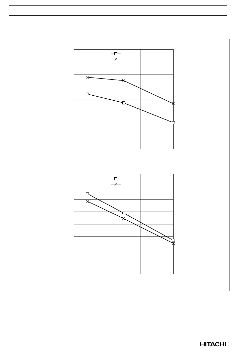
Characteristic Curves
PF00105A
60
Pin=+7dBm
Vdd=4.6V
Pout=1W
55
50
(%)
T
η
45
40
−50 100
1.6
Pin=+7dBm
Vdd=4.6V
1.5
Vapc=2.9V
ηT vs. Tc
824MHz
849MHz
050
Tc (°C)
Pout vs. Tc
824MHz
849MHz
1.4
1.3
1.2
Pout(1) (W)
1.1
1
0.9
0.8
−50 100
050
Tc (°C)
3
Page 4

PF00105A
31.8
Vdd=4.6V
Vapc=2.9V
Tc=−30°C
31.6
31.4
Pout(1) (dBm)
31.2
31
410
31.4
Vdd=4.6V
Vapc=2.9V
Tc=25°C
Pout vs. Pin (1)
824MHz
836.5MHz
849MHz
68
Pin (dBm)
Pout vs. Pin (2)
824MHz
836.5MHz
849MHz
31.2
31
Pout(1) (dBm)
30.8
30.6
410
68
Pin (dBm)
4
Page 5

PF00105A
31
Vdd=4.6V
Vapc=2.9V
Tc=60°C
30.8
30.6
Pout(1) (dBm)
30.4
30.2
410
700
Pin=+7dBm
Vdd=4.6V
Tc=−30°C
600
500
824MHz
836.5MHz
849MHz
Pout vs. Pin (3)
824MHz
836.5MHz
849MHz
68
Pin (dBm)
Id vs. Vapc (1)
400
Id (mA)
300
200
100
0
0 4.542.532.521.510.5 5
Vapc (V)
5
Page 6

PF00105A
700
Pin=+7dBm
Vdd=4.6V
Tc=25°C
600
500
400
Id (mA)
300
200
100
0
700
600
500
824MHz
836.5MHz
849MHz
0 4.542.532.521.510.5 5
Pin=+7dBm
Vdd=4.6V
Tc=60°C
824MHz
836.5MHz
849MHz
Id vs. Vapc (2)
Vapc (V)
Id vs. Vapc (3)
400
Id (mA)
300
200
100
0
0 4.542.532.521.510.5 5
Vapc (V)
6
Page 7

PF00105A
40
Pin=+7dBm
Vdd=4.6V
30
Tc=−30°C
20
10
0
Pout (dBm)
−10
−20
−30
−40
0 4.542.532.521.510.5 5
40
Pin=+7dBm
Vdd=4.6V
30
Tc=25°C
Pout vs. Vapc (1)
Vapc (V)
Pout vs. Vapc (2)
824MHz
836.5MHz
849MHz
20
10
0
Pout (dBm)
−10
−20
−30
−40
0 4.542.532.521.510.5 5
Vapc (V)
824MHz
836.5MHz
849MHz
7
Page 8

PF00105A
40
Pin=+7dBm
Vdd=4.6V
30
Tc=60°C
20
10
0
Pout (dBm)
−10
−20
−30
−40
0 4.542.532.521.510.5 5
34
f=824MHz
Pin=+7dBm
Tc=25°C
33
Vapc=2.5V
Vapc=2.9V
Vapc=4.6V
Pout vs. Vapc (3)
Vapc (V)
Pout vs. Vdd (1)
824MHz
836.5MHz
849MHz
32
31
Pout (dBm)
30
29
3.5 5.554.546
Vdd (V)
8
Page 9

PF00105A
34
f=836.5MHz
Pin=+7dBm
Tc=25°C
33
32
31
Pout (dBm)
30
29
3.5 5.554.546
34
33
Vapc=2.5V
Vapc=2.9V
Vapc=4.6V
f=849MHz
Pin=+7dBm
Tc=25°C
Vapc=2.5V
Vapc=2.9V
Vapc=4.6V
Pout vs. Vdd (2)
Vdd (V)
Pout vs. Vdd (3)
32
31
Pout (dBm)
30
29
3.5 5.554.546
Vdd (V)
9
Page 10

PF00105A
Package Dimensions
Unit: mm
43G
(7.8)
8.0 ± 0.3
12
G
(Upper side)
13.75 ± 0.3
12
(3.7)
(3.7)
43GG
(1.8) (1.8) (1.8) (1.8)
(1.3) (1.3)
(2.225) (2.975)
(6.875)
13.75 ± 0.3
(Bottom side)
(9.6)
(1.6)
G
G
GG
(6.875)
(2.1)(2.1)
1.8 ± 0.2
8.0 ± 0.3
3
G
G
4
G
1
(0.6)
Remark:
Coplanarity of bottom side of terminals
are less than 0 ± 0.1mm.
Hitachi Code
JEDEC
EIAJ
Weight
(reference value)
RF-K
2
G
10
Page 11

Cautions
1. Hitachi neither warrants nor grants licenses of any rights of Hitachi’s or any third party’s patent,
copyright, trademark, or other intellectual property rights for information contained in this document.
Hitachi bears no responsibility for problems that may arise with third party’s rights, including
intellectual property rights, in connection with use of the information contained in this document.
2. Products and product specifications may be subject to change without notice. Confirm that you have
received the latest product standards or specifications before final design, purchase or use.
3. Hitachi makes every attempt to ensure that its products are of high quality and reliability. However,
contact Hitachi’s sales office before using the product in an application that demands especially high
quality and reliability or where its failure or malfunction may directly threaten human life or cause risk
of bodily injury, such as aerospace, aeronautics, nuclear power, combustion control, transportation,
traffic, safety equipment or medical equipment for life support.
4. Design your application so that the product is used within the ranges guaranteed by Hitachi particularly
for maximum rating, operating supply voltage range, heat radiation characteristics, installation
conditions and other characteristics. Hitachi bears no responsibility for failure or damage when used
beyond the guaranteed ranges. Even within the guaranteed ranges, consider normally foreseeable
failure rates or failure modes in semiconductor devices and employ systemic measures such as failsafes, so that the equipment incorporating Hitachi product does not cause bodily injury, fire or other
consequential damage due to operation of the Hitachi product.
5. This product is not designed to be radiation resistant.
6. No one is permitted to reproduce or duplicate, in any form, the whole or part of this document without
written approval from Hitachi.
7. Contact Hitachi’s sales office for any questions regarding this document or Hitachi semiconductor
products.
Hitachi, Ltd.
Semiconductor & Integrated Circuits.
Nippon Bldg., 2-6-2, Ohte-machi, Chiyoda-ku, Tokyo 100-0004, Japan
Tel: Tokyo (03) 3270-2111 Fax: (03) 3270-5109
URL NorthAmerica : http:semiconductor.hitachi.com/
For further information write to:
Hitachi Semiconductor
(America) Inc.
179 East Tasman Drive,
San Jose,CA 95134
Tel: <1> (408) 433-1990
Fax: <1>(408) 433-0223
Europe : http://www.hitachi-eu.com/hel/ecg
Asia (Singapore) : http://www.has.hitachi.com.sg/grp3/sicd/index.htm
Asia (Taiwan) : http://www.hitachi.com.tw/E/Product/SICD_Frame.htm
Asia (HongKong) : http://www.hitachi.com.hk/eng/bo/grp3/index.htm
Japan : http://www.hitachi.co.jp/Sicd/indx.htm
Hitachi Europe GmbH
Electronic components Group
Dornacher Stra§e 3
D-85622 Feldkirchen, Munich
Germany
Tel: <49> (89) 9 9180-0
Fax: <49> (89) 9 29 30 00
Hitachi Europe Ltd.
Electronic Components Group.
Whitebrook Park
Lower Cookham Road
Maidenhead
Berkshire SL6 8YA, United Kingdom
Tel: <44> (1628) 585000
Fax: <44> (1628) 778322
Hitachi Asia Pte. Ltd.
16 Collyer Quay #20-00
Hitachi Tower
Singapore 049318
Tel: 535-2100
Fax: 535-1533
Hitachi Asia Ltd.
Taipei Branch Office
3F, Hung Kuo Building. No.167,
Tun-Hwa North Road, Taipei (105)
Tel: <886> (2) 2718-3666
Fax: <886> (2) 2718-8180
Copyright ' Hitachi, Ltd., 1999. All rights reserved. Printed in Japan.
Hitachi Asia (Hong Kong) Ltd.
Group III (Electronic Components)
7/F., North Tower, World Finance Centre,
Harbour City, Canton Road, Tsim Sha Tsui,
Kowloon, Hong Kong
Tel: <852> (2) 735 9218
Fax: <852> (2) 730 0281
Telex: 40815 HITEC HX
 Loading...