

Datasheet PEEL18CV8ZT-25, PEEL18CV8ZTI-25, PEEL18CV8ZJ-25, PEEL18CV8ZJI-25, PEEL18CV8ZP-25 Datasheet (ICT)
...Page 1
Commercial
PEEL™ 18CV8Z
CMOS Programmable Electrically Erasable Logic Device
Features
■
Ultra Low Power Operation
- Vcc = 5 Volts ±10%
- Icc = 10 µA (typical) at standby
- Icc = 2 mA (typical) at 1 MHz
■
CMOS Electrically Erasable T echnolog y
- Superior factory testing
-
Reprogrammable in plastic package
-
Reduces retrofit and development costs
■
Application Versatility
-
Replaces random logic
-
Super set of standard PLDs
-
Pin-to-pin compatible with 16V8
-
Ideal for use in power-sensitive systems
General Descri p ti on
The PEEL™18CV8Z is a Programmable Electrically Erasable
Logic (PEEL™) SPLD (Simple Programmable Logic Device)
that features ultra-low, automatic “zero” power-down operation.
The “zero power” (100 µA max. Icc) power-down mode makes
the PEEL™18CV8Z ideal for a broad range of battery-powered
portable equipment applications, from hand-held meters to PCMCIA modems. EE-reprogrammability provides both the convenience of fast reprogramming for product development and quick
product personalization in manufacturing, including Engineering
Change Orders.
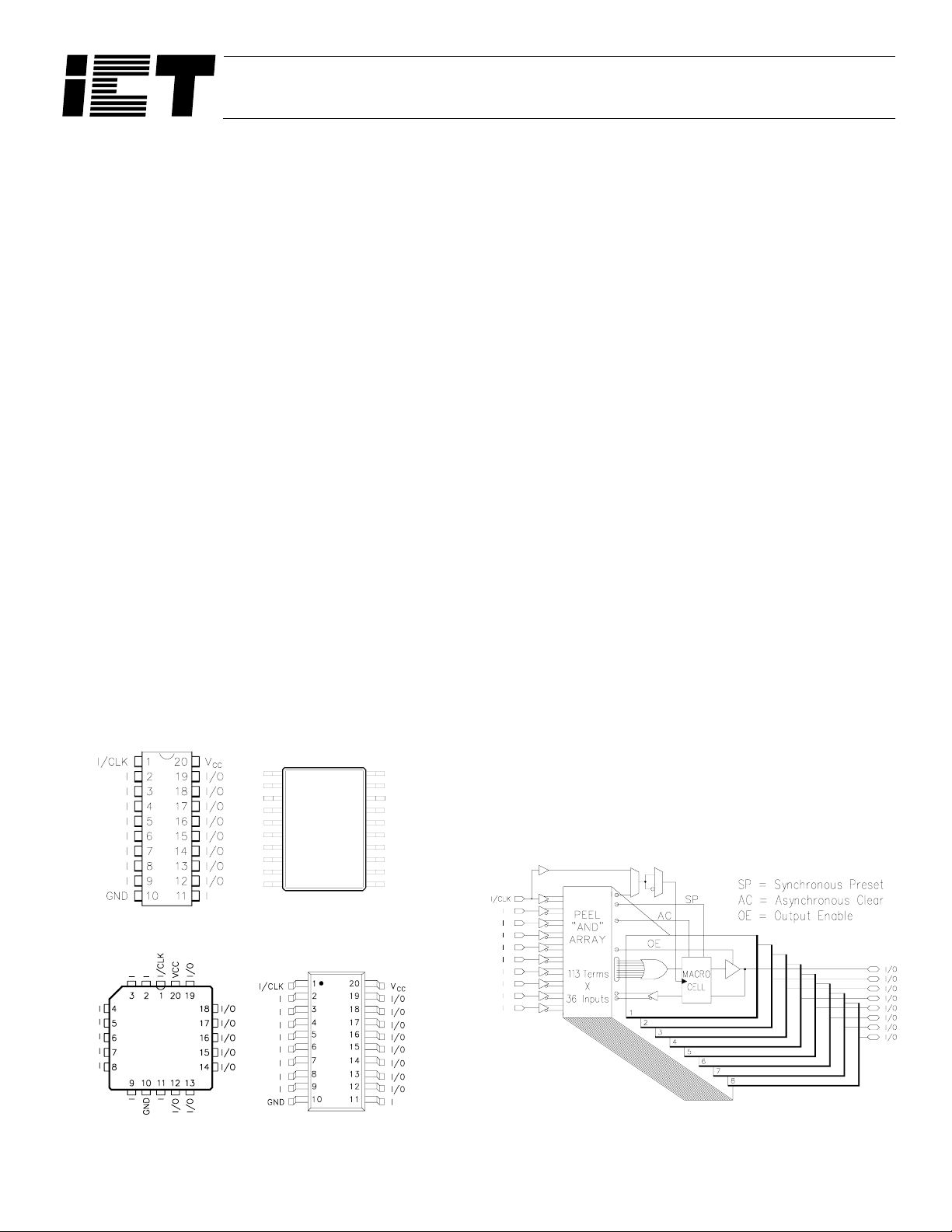
Figure 7 Pin Configuration
1
I/CLK
GND
2
I
3
I
4
I
5
I
6
I
7
I
8
I
9
I
10
VCC
20
I/O
19
I/O
18
I/O
17
I/O
16
I/O
15
I/O
14
I/O
13
I/O
12
I
11
-25
■
Architectural Flexibility
-
Enhanced architecture fits in more logic
-
113 product terms x 36 input AND array
-
10 inputs an d 8 I/O pins
-
12 possible macrocell configurations
-
Asynchronous clear, Synchronous preset
-
Independent output enables
-
Programmable clock; pin 1 or p-term
-
Programmable clock polarity
-
20 Pin DIP/SOIC/TSSOP and PL CC
The PEEL™18CV8Z is logically and functionally similar to
ICT’s 5 Volt PEEL™18CV8 and 3 Volt PEEL™18LV8Z. The
differences between the PEEL™18CV8Z and PEEL™18CV8
include the addition of programmable clock polarity, a product
term clock, and variable width product terms in the AND/OR
Logic Array.
Like the PEEL™18CV8, the PEEL™18CV8Z is logical superset
of the industry standard PAL16V8 SPLD. The PEEL™18CV8Z
provides additional architectural features that allow more logic to
be incorporated into the design. ICT’s JEDEC file translator
allows easy conversion of existing 20 pin PLD designs to the
PEEL™18CV8Z architecture without the need for redesign. The
PEEL™18CV8Z architecture allows it to replace over twenty
standard 20-pin DIP, SOIC, TSSOP and PLCC packages.
Figure 8 Block Diagram
CLK MUX (Optional)
DIP
PLCC
TSSOP
SOIC
™
1 of 10
Page 2
PEELTM 18CV8Z-25
I/CLK
(OPTIONAL)
ASYNCHRONOUS CLEAR
(TO ALL MACROCELLS)
MACRO
CELL
19
I/O
03478111215161920232427283132
112
0
1
2
9
35
1
10
11
18
17
I/O
I/O
MACRO
20
2
I
21
22
CELL
MACRO
CELL
33
3
I
34
35
16
MACRO
I/O
CELL
48
4
I
49
50
I/O
MACRO
15
CELL
65
5
I
66
67
I/O
MACRO
14
CELL
82
6
I
83
84
13
MACRO
I/O
CELL
97
7
I
98
99
12
MACRO
I/O
CELL
110
8
I
111
9
I
SYNCHRONOUS PRESET
(TO ALL MACROCELLS)
11
I
Figure 9 PEEL™18CV8Z Logic Array Diagram
2 of 10
Page 3

PEELTM 18CV8Z-25
Function Description
The PEEL™18CV8Z implements logic functions as sum-ofproducts expressions in a programmable-AND/fixed-OR logic
array. User-defined functions are created by programming the
connections of input signals into the array. User-configurable
output structures in the form of I/O macrocells further increase
logic flexibility.
Architecture Overview
The PEEL™18CV8Z architecture is illustrated in the block diagram of Figure 8. Ten dedicated inputs and 8 I/Os provide up to
18 inputs and 8 outputs for creation of logic functions. At the
core of the device is a programmable electrically-erasable AND
array that drives a fixed OR array. With this structure, the
PEEL™18CV8Z can implement up to eight sum-of-products
logic expressions.
Associated with each of the eight OR functions is an I/O macrocell that can be independently programmed to one of 12 different
configurations. The programmable macrocells allow each I/O to
be used to create sequential or combinatorial logic functions of
active-high or active-low polarity, while providing three different
feedback paths into the AND array.
AND/OR Logic Array
The programmable AND array of the PEEL™1 8CV8Z (sh own in
Figure 9) is formed by input lines intersecting product terms. The
input lines and product terms are used as follows:
■
36 Input Lines:
– 20 input lines carry the true and complement of the signals
applied to the 10 input pins
– 16 additional lines carry the true and complement values of
feedback or input signals from the 8 I/Os
effect on the output function).
Variable Product Term Distribution
The PEEL™18CV8Z provides 113 product terms to drive the
eight OR functions. These product terms are distributed among
the outputs in groups of 8, 10, 12, 14, and 16 to form l ogical s ums
(see Figure 9). This distribution allows optimum use of the
device resources.
Programmable I/O Macrocell
The unique twelve-configuration output macrocell prov ides complete control over the architecture of each output. The ability to
configure each output independently lets you to tailor the configuration of the PEEL™18CV8Z to the precise requirements of
your design.
Macrocell Architecture
Each I/O macrocell, as shown in Figure 9, consists of a D-type
flip-flop and two signal-select multiplexers. The co nfiguration of
each macrocell is determined by the four EEPROM bits controlling these multiplexers. These bits determine output polarity, output type (registered or non-registered) and input-feedback path
(bidirectional I/O, combinatorial feedback). Refer to Table 1 for
details.
Equivalent circuits for the twelve macrocell configurations are
illustrated in Figure 11. In addition to emulating the four PALtype output structures (configurations 3, 4, 9, and 10), the macrocell provides eight additional configurations. When creating a
PEEL™ device design, the desired macrocell configuration is
generally specified explicitly in the design file. When the desi gn
is assembled or compiled, the macrocell configuration bits are
defined in the last lines of the JEDEC programming file.
■
113 product terms:
102 product terms are used to form sum of product functions
–
– 8 output enable terms (one for each I/O)
– 1 global synchronous pr eset term
– 1 global asynchronous clear term
– 1 programmable clock term
At each input-line/product-term intersection, there is an
EEPROM memory cell that determines whether or not there is a
logical connection at that intersection. Each product term is
essentially a 36-input AND gate. A product term that is connected to both the true and complement of an input signal will
always be FALSE and thus will not affect the OR function that it
drives. When all the connections on a product term are opened, a
“don’t care” state exists and that term will always be TRUE.
When programming the PEEL™18CV8Z, the device programmer first performs a bulk erase to remove the previous pattern.
The erase cycle opens every logical connection in the array. The
device is configured to perform the user-defined function by programming selected connections in the AND array. (Note that
PEEL™ device programmers automatically program all of the
connections on unused product terms so that they will have no
Output Type
The signal from the OR array can b e fed directly to th e ou tput pin
(combinatorial function) or latched in the D-type flip-flop (registered function). The D-type flip-flop latches data on the rising
edge of the clock and is controlled by the global preset and clear
terms. When the synchronous preset term is satisfied, the Q output of the register is set HIGH at the next rising edge of the clock
input. Satisfying the asynchronous clear sets Q LOW, regardless
of the clock state. If both terms are satisfied simultaneously, the
clear will override the preset.
Output Polarity
Each macrocell can be configured to implement active-high or
active-low logic. Programmable polarity eliminates the need for
external inverters.
Output Enable
The output of each I/O macrocell can be enabled or disabled
under the control of its associated programmable output enable
product term. When the logical conditions programmed on the
output enable term are satisfied, the output signal is pro pagated to
3 of 10
Page 4

PEELTM 18CV8Z-25
the I/O pin. Otherwise, the output buffer is switched into the
high-impedance state.
Under the control of the output enable term, the I/O pin can function as a dedicated input, a dedicated output, or a bi-directional I/
O. Opening every connection on the output enable te rm will permanently enable the output buff er and yield a dedicated output.
Conversely, if every connection is intact, the enable term will
always be logically false and the I/O will function as a dedicated
input.
Input/Feedback Select
The PEEL™18CV8Z macrocell also provides control over the
feedback path. The input/feedback signal associated with each I/
O macrocell can be obtained from three different locations; from
the I/O input pin, from the Q
output of the flip-flop (registered
feedback), or directly from the OR gate (combinatorial feedback).
Bi-directional I/O
The input/feedback signal is taken from the I/O pin when using
the pin as a dedicated input or as a bi-directional I/O. (Note that it
is possible to create a registered output function with a bi-directional I/O, refer to Figure 9).
Combinatorial Feedback
The signal-select multiplexer gives the macrocell the ability to
feedback the output of the OR gate, bypassing the output buffer,
regardless of whether the output function is registered or combinatorial. This feature allows the creation of asynchronous latches,
even when the output must be disabled. (Refer to configurations
5, 6, 7, and 8 in Figure 11.)
tion, registered feedback allows for the internal latching of states
without giving up the use of the external output.
Programmable Clock Options
A unique feature of the PEEL™18CV8Z is a programmable
clock multiplexer that allows the user to select true or co mplement forms of either input pin or product-term clock sources.
Zero Power Feature
The CMOS PEEL™18CV8Z features “Zero-Power” standby
operation for ultra-low power consumption. With the “ZeroPower” feature, transition- detect ion ci rcu itr y mon i tors the input s ,
I/Os (including CLK) and feedbacks. If these signals do not
change for a period of time greater than approximately two t
PD
’s,
the outputs are latched in their current state and the device automatically powers down. When the next signal transition is
detected, the device will “wake up” for active operation until the
signals stop switching long enough to trigger the next powerdown. (Note that the tPD is approximately 5 ns. slower on the
first transition from sleep mode.)
As a result of the “Zero-Power” feature, significant power savings can be realized for combinatorial or sequential operations
when the inputs or clock change at a modest rate. See Figure 5.
Figure 10 Typical ICC vs. Input Clock Frequency
for the 18CV8Z
100
10
Figure 9 Block Diagram of the PEEL™18CV8Z
I/O Macrocell
Registered Feedback
Feedback also can be taken from the register, regardless of
whether the output function is programmed to be combinatorial
or registered. When implementing a combinatorial output func-
1
ICC in mA.
0.1
0.01
0.001
0.001
0.01 0.1 1 10
Frequency in MHz
4 of 10
Page 5

PEELTM 18CV8Z-25
Configuration
Input/Feedback Select Output Select
# A B C D
10010
21010 Active High
30100
41100 Active High
50011
61011 Active High
70111
81111 Active High
90000
10 1000 Active High
11 0110
12 1110 Active High
Bi-directional I/O
Combinatorial Feedback
Register Feedback
Register
Combinatorial
Register
Combinatorial
Register
Combinatorial
Active Low
Active Low
Active Low
Active Low
Active Low
Active Low
5 of 10
Page 6

PEELTM 18CV8Z-25
Design Security
The PEEL™18CV8Z provides a special EEPROM security bit
that prevents unauthorized reading or copying of designs programmed into the device. The security bit is set by the PLD programmer, either at the conclusion of the programming cycle or as
a separate step, after the device has been programmed. Once the
security bit is set it is impossible to verify (read) or program the
PEEL™ until the entire device has first been erased with the
bulk-erase function.
Signature Word
The signature word feature allows a 64-bit code to be programmed into the PEEL™18CV8Z if the software option is used.
The code can be read back even after the security bit has been set.
The signature word can be used to identify the pattern programmed into the device or to record the design revision, etc.
Programming Support
ICT’s JEDEC file translator allows easy conversion of existing
20 pin PLD designs to the PEEL™18CV8Z, without the need for
redesign. ICT supports a broad range of popular third party
design entry systems, including Data I/O Synario and Abel, Logical Devices CUPL and others. ICT also offers (for free) its proprietary PLACE software, an easy-to-use entry level PC-based
software development system.
Programming support includes all the popular third party programmers; Data I/O, Logical Devices, and numerous others. ICT
also provides a low cost development programmer system, the
PDS-3.
6 of 10
Page 7

PEELTM 18CV8Z-25
This device has been designed and tested for the specified operating ranges. Proper operation outside of these levels is not guaranteed. Exposure to absolute maximum ratings may cause
Absolute Maximum Ratings
Symbol Parameter Conditions Rating Unit
CC
V
I
, V
V
O
I
ST
T
LT
T
Supply Voltage Relative to Grou nd -0.5 to + 7.0 V
O
Voltage A ppl ied to Any Pin
Output Current Per Pin (IOL, IOH)±25mA
Storage Temperature -65 to +150 °C
Lead Temperature Soldering 10 Seconds +300 °C
2
Relative to Ground
Operating Range
Symbol Parameter Conditions Min Max Unit
permanent damage.
1
-0.5 to VCC + 0.6 V
Vcc Supply Voltage
T
T
A
R
T
F
T
RVCC
Ambient Temperature
Clock Rise Time See Note 3. 20 ns
Clock Fall Time See Note 3. 20 ns
V
Rise Time
CC
Commercial 4.75 5.25 V
Industrial 4.5 5.5 V
Commercial 0 +70 °C
Industrial -40 +85 °C
See Note 3. 250 ms
D.C. Electrical Characteristics Over the operating range (Unless otherwise specified)
Symbol Parameter Conditions Min Max Unit
OH
V
V
C
V
V
V
V
I
CCS
I
CC
I
C
OUT
OHC
OL
OLC
IH
IL
IL
I
SC
IN
9
10
7
Output HIGH Voltage - TTL VCC = Min, IOH = -4.0 mA 2.4 V
Output HIGH Voltage - CMOS VCC = Min, IOH = -10.0 µA VCC - 0.3 V
Output LOW Voltage - TTL VCC = Min, IOL = 16.0 mA 0.5 V
Output LOW Voltage - CMOS VCC = Min, IOL = 10.0 µA 0.15 V
Input HIGH Voltage 2.0 VCC + 0.3 V
Input LOW Voltage -0.3 0.8 V
Input and I/O Leakage Curre nt VCC = Max, GND ≤ VIN ≤ VCC, I/O = High Z ±10 µA
Output Short Circuit Current VCC = Max, VO = 0.5V, TA = 25°C -30 -135 mA
VCC Current, Standby
VCC Current, f=1MHz
Input Capacitance
7
Output Capacitance 12 pF
VIN = 0V or V
VIN = 0V or V
TA = 25 ° C , VC C = Ma x @ f = 1 MHz
CC
, All Outputs disabled
CC
, All Outputs disabled
4
4
10 (typ) 100 µA
2 (typ) 5 mA
6pF
7 of 10
Page 8

A.C. Electrical Characteristics
Over the operating range
8
PEELTM 18CV8Z-25
Symbol Parameter
PD
t
t
t
CO1
t
CO2
t
t
t
t
CL
t
t
MAX1
f
MAX2
f
MAX3
f
AW
t
t
t
RESET
t
OE
OD
CF
SC
HC
, t
CP
AP
AR
CH
Input5 to non-registered output
Input5 to output enable
Input5 to output disable
Clock to Output 15 ns
Clock to comb. output delay via internal registered feedback 35 ns
Clock to Feedback 9 ns
Input5 or feedback setup to cloc k
Input5 hold after clock
Clock low time, cloc k hi gh ti m e
Min clock per i od Ext (tSC + t
Internal fe edback (1/tSC+tCF)
External Feedback (1/tCP)
No Feedback (1/tCL+tCH)
Asynchronous Reset Pulse Width 25 ns
Input5 to Asynchronous Reset
Asynchronous Reset recov er y time 25 ns
Power-on reset time for registers in clear state
6
6
8
CO1
)30ns
11
11
11
-25 / I-25
Units
Min Max
25 ns
25 ns
25 ns
15 ns
0ns
13 ns
41.6 MHz
33.3 MHz
38.4 MHz
25 ns
12
5µs
Switching Waveforms
Registered Feedback,
Synchronous Preset
Notes:
1. Minimum DC input is -0.5V, however, inputs may undershoot to -2.0V for periods less than 20 ns.
I
2. V
and VO are not specified for program/verify operation.
3. Test Points for Clock and V
levels.
4. I/O pins are 0V and V
5. “Input” refers to an inpu t pi n signal.
OE
6. t
is measured from input transition to V
OD
is measured from input tra nsition to VOH-0.1V or VOL+0.1V; V
T
7. Capacitances are tested on a sample basis.
Inputs, I/O,
Clock
Asynchronous
Reset
Registered
Outputs
Combinatorial
Outputs
CC
in tR and tF are referenced at the 10 % and 90%
CC
.
REF
±0.1V,
REF=VL.
8. Test conditions assume: signal transition times of 3ns or less from the 10% and
90% points, timing reference levels of 1.5V (Unless otherwise spec ifi e d).
9. Test one output at a time for a duration of less than 1 second.
CC
for a typical a p plication: This paramete r is tested with the d evice pro-
10. I
grammed as an 8-bi t Co unter.
11. Parameters are not 100% tested. Specifications are based on initial characterization and a re te ste d a fter an y de sig n pr oce s s modi fi ca tion th at mi gh t affect operational frequency.
12. All input at GND.
8 of 10
Page 9

PEEL™ Device and Array Test Loads
5.0 VStandard
Load
Thevenin
Equivalent
PEELTM 18CV8Z-25
L
V
Output
L
C
R2
Output
Technology R1 R2 R
CMOS 480kΩ 480kΩ 228kΩ 2.375V 33 pF
TTL 235Ω 159Ω 95Ω 2.02V 33 pF
R1
L
R
CL
L
V
L
Ordering Information
Part Number Speed Temperature Package
PEEL18CV8ZP-25 25ns Commercial 20-pin Plastic DIP
PEEL18CV8ZJ-25 25ns Commercial 20-pin PLCC
PEEL18CV8ZS-25 25ns Commercial 20-pin SOIC
PEEL18CV8ZT-25 25ns Commercial 20-pin TSSOP
PEEL18CV8ZPI-25 25ns Industrial 20-pin Plastic DIP
PEEL18CV8ZJI-25 25ns Industrial 20-pin PLCC
PEEL18CV8ZSI-25 25ns Industrial 20-pin SOIC
PEEL18CV8ZTI-25 25ns Industrial 20-pin TSSOP
C
L
Part Number
PEEL™18CV8Z
Package
P = 20-pin Plastic 300mil DIP
J = 20-pin Plastic (J) Leaded Chip Carrier (PLCC)
S = 20-pin SOIC 300 mil Gullwing
T = 20-pin TSSOP 170 mil
Device
Suffix
PI-25
Speed
–25 = 25ns tpd
Temperature Grade
(Blank) = Commercial 0 to 70° C
I = Industrial –40 to +85° C
9 of 10
Page 10

 Loading...