

Datasheet PDSP16488AA0, PDSP16488AAC, PDSP16488AB0, PDSP16488AC, PDSP16488ACBR Datasheet (MITEL)
...Page 1
PDSP16488A
Single Chip 2D Convolver with Integral Line Delays
Advance Information
Supersedes version in 1996 Media IC Handbook, HB4599-1.0 DS3713 - 6.4 December 1997
and the PDSP16488A MA data sheet, DS3742
The PDSP16488A is a fully integrated, application specific,
image processing device. It performs a two dimensional convolution between the pixels within a video window and a set of
stored coefficients. An internal multiplier accumulator array can
be multi-cycled at double or quadruple the pixel clock rate. This
then gives the window size options listed in Table 1.
An internal 32kbit RAM can be configured to provide either
four or eight line delays. The length of each delay can be
programmed to the users requirement, up to a maximum of 1024
pixels per line. The line delays are arranged in two groups,which
may be internally connected in series or may be configured to
accept separate pixel inputs. This allows interlaced video or
frame to frame operations to be supported.
The 8-bit coefficients are also stored internally and can be
downloaded from a host computer or from an EPROM. No
additional logic is required to support the EPROM and a single
device can support up to 16 convolvers.
The PDSP16488A contains an expansion adder and delay
network which allows several devices to be cascaded. Convolvers with larger windows can then be fabricated as shown in
Table 2.
Intermediate 32-bit precision is provided to avoid any danger
of overflow, but the final result will not normally occupy all bits.
The PDSP16488A thus provides a gain control block in the
output path, which allows the user to align the result to the most
significant end of the 32-bit word.
Table 2 PDSP16488As needed to implement typical window sizes
Pixel
size
Width
Window size
Depth
Maximum pixel
rate (MHz)
Line delays
8
8
8
16
16
4
8
8
4
8
4
4
8
4
4
20
20
10
20
10
431024
431024
83512
43512
43512
Table 1 Single PDSP16488A configurations
Max.
pixel
rate
(MHz)
Pixel
size
333
535 737 939 11311 15315 23323
No. of PDSP16488As for N3N window size
10
10
20
20
40
40
8
16
8
16
8
16
1
1
1
1
1
2
1
2
2
4
4*
-
1
2
2
4
4*
-
4
-
6
-
-
-
4
-
6
-
-
-
4
-
8
-
-
-
9
-
-
-
-
-
*Maximum rate is limited to 30MHz by line store expansion delays
ORDERING INFORMATION
Commercial (0°C to 170°C)
PDSP16488A / C0 / AC (PGA)
Industrial (240°C to 185°C)
PDSP16488A / B0 / AC (PGA)
PDSP16488A / B0 / GC (QFP)
Military (255°C to 1125°C)
PDSP16488A / A0 / AC (PGA)
PDSP16488A / A0 / GC (QFP)
PDSP16488A / MA / ACBR (PGA) MIL-STD-883 Class B*
PDSP16488A / MA / GCPR (QFP) MIL-STD-883 Class B*
*See Notes following Static Electrical CharacteristicsTable
Note: PDSP16488A devices are not guaranteed to cascade with
PDSP16488 devices. Mitel Semiconductor do not recommend
that PDSP16488A be mixed with PDSP16488 devices in a single
equipment design. The PDSP16488A requires external pullup
resistors in EPROM Mode (see Static Electrical Characteristics).
FEATURES
■ The PDSP16488A is a replacement for the
PDSP16488 (see Note below)
■ 8 or 16-bit Pixels with rates up to 40 MHz
■ Window Sizes up to 838 with a Single Device
■ Eight Internal Line Delays
■ Supports Interlace and Frame-to-Frame Operations
■ Coefficients Supplied from an EPROM or Remote Host
■ Expandable in both X and Y for Larger Windows
■ Gain Control and Pixel Output Manipulation
■ 84-pin PGA or 132-pin QFP Package Options
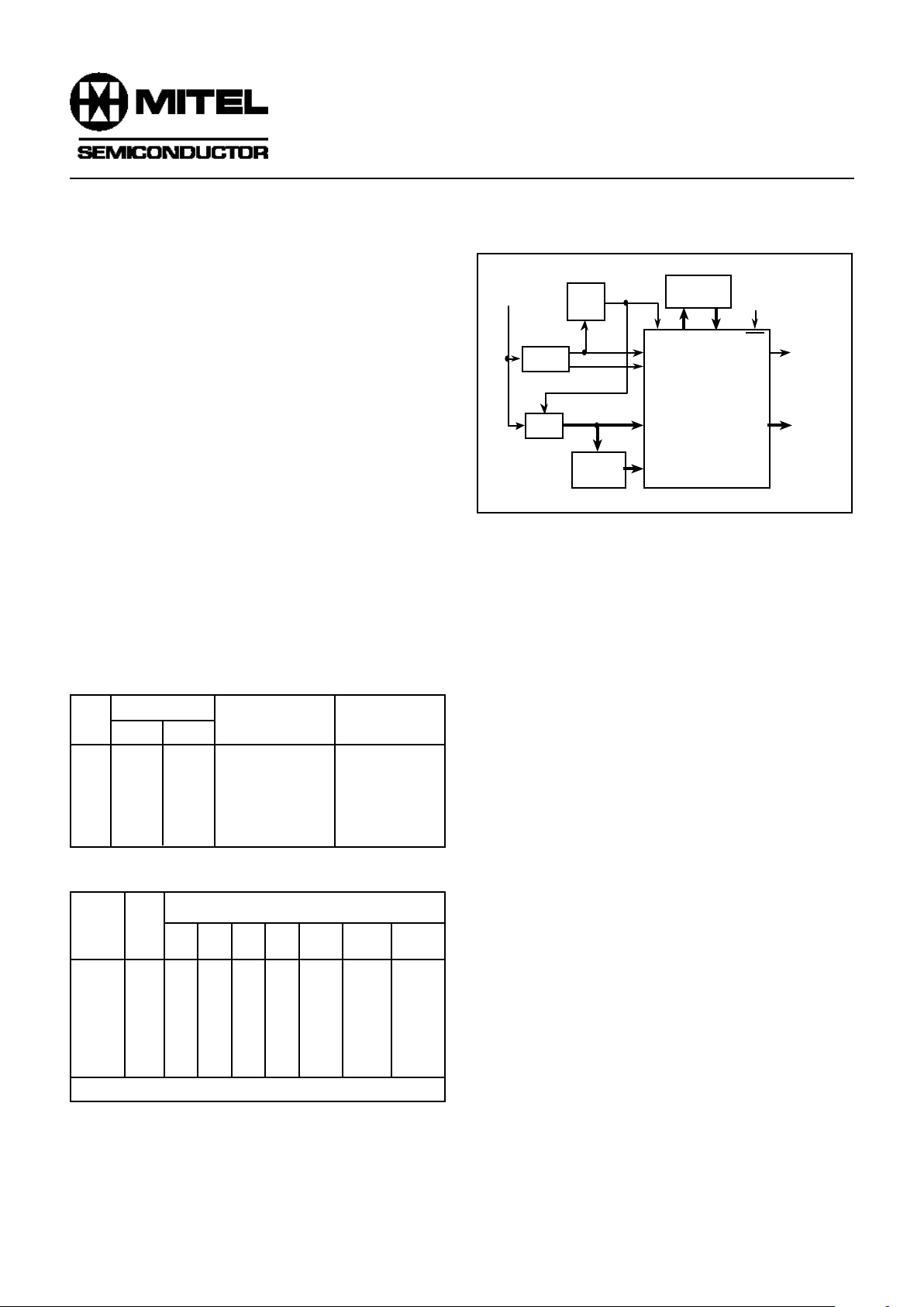
Fig. 1 Typical stand-alone real time system
PDSP16488A
EPROM
ADDR DATA
POWER
ON
RESET
DELAYED
SYNC
OUTPUT
DATA
RES
DELOP
CLK
HRES
BYPASS
SYNC
EXTRACT
COMPOSITE
DATA
PIXEL
CLOCK
GEN
ADC
OPTIONAL
FIELD
DELAY
IP7:0
L7:0
D15:0
SYNC
ODD FIELD
Page 2
2
Type
Input
I/O
Input
Input
Dual
function
Output
Output
Input
Output
I/O
Input
Input
I/O
Input
Output
Output
Input
Input
Input
Input
Outputs
Outputs
Power
Power
Signal
IP7:0
L7:0
BYPASS
HRES
X15:0
D15:0
PC1
PC0
DELOP
DS
CE
R/W
PROG
CLK
BIN
OVR
RES
SINGLE
MASTER
OEN
CS3:0
F1:0
V
DD
GND
Table 3 Signal descriptions
Description
Pixel data input to the first line delay (most significant byte in 16-bit mode).
Pixel data input to the second group of line delays. (least significant byte in 16-bit mode). Alterna-
tively an output from the last line delay when the appropriate mode bit is set.
The first line delay in the first group is bypassed when this input is high. No internal pullup resistor.
Resets the line delay address pointers when high. Normally the composite sync signal in real time
applications. In non real time systems it defines a frame store update period, when low.
Address/data connections from a Master or Single device to the external coefficient source,
with X15 defining EPROM or Host support. Otherwise they provide the expansion data input.
Signed 16-bit scaled data or multiplexed 32-bit intermediate data. During intermediate transfers the
most significant half is valid when the clock is low, and the least significant half when clock is high.
During programming a Master device outputs a timing strobe on this pin. This is passed down
the chain in a multiple device system, using the
PC0
input on the next device.
This pin is used in conjunction with
PC1
in multiple device systems. It terminates the write strobe
from a Master device which is EPROM supported.
This output provides a version of the HRES input which has been delayed by an amount defined by
the user.
The data strobe from a host computer, active low. This pin will be an output from an EPROM
supported Master device which provides strobes to the remaining devices.
An active low enable which is internally gated with
R/W
andDSto perform reads or writes to the
internal registers. In a Single or Master device, which is supported from an EPROM, the
bottom 72 addresses are always used andCEis not needed.CEcan then be used to initiate a
new register load sequence after the power on load sequence.
Read / not write line from the host CPU. When an EPROM is used this pin should be tied low.
This pin is normally an input which signifies that registers are to be changed or examined. It is,
however, an output from an EPROM supported Single or Master device indicating to the rest
of the system that registers are being updated.
Clock. All events are triggered on the rising edge of CLK, except the latching of least significant
expansion inputs . Internally the clock can be multiplied by two or four in order to increase the
effective number of multipliers.
This output indicates the result from the internal comparison. A high value indicates that the pixel
was greater than the internal threshold. The output is only valid from the last device in a chain.
When high this output indicates that there has been a gain control overflow.
Active low power on reset signal.
Tied to ground to indicate a Single device system. Internal pullup resistor.
Tied to ground to indicate the Master device in a multiple device system. Must be left open circuit
in a Single device system. Internal pullup resistor.
Output enable signal. Active low.
Four address bits from a Master specifying one of sixteen devices in a multiple device system.
Must be externally decoded to provide chip enables for the additional devices.
These bits indicate the field selection given by the gain control auto select logic. The same coding
as that used for Control Register bits C5:4 is used.
15V supply. All VDD pins must be connected.
0V supply. All GND pins must be connected.
Page 3
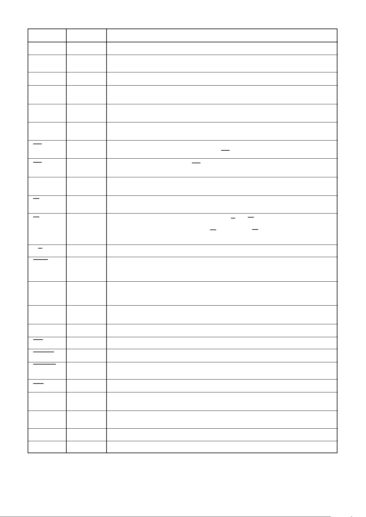
3
838
ARRAY
OF
MACs
COEFFICIENT
STORE (64)
3 LINE
DELAYS
4 LINE
DELAYS
1 LINE
DELAY
Y
DELAY
Y
DELAY
BYPASS
X
DELAY
CS3:0RES
CONTROL
PC1
CONTROL
REGISTERS
COMPARATOR
D15:0
BIN
OVR
CLK OEN
PROG
MASTER
SINGLE
DELOP
HRES
PC0R/WDSCE
BIDIRECTIONAL
MULTIPURPOSE
DATA BUS X15:0
IP7:0
L7:0
F1:0
Fig. 2 Functional block diagram
Page 4
4
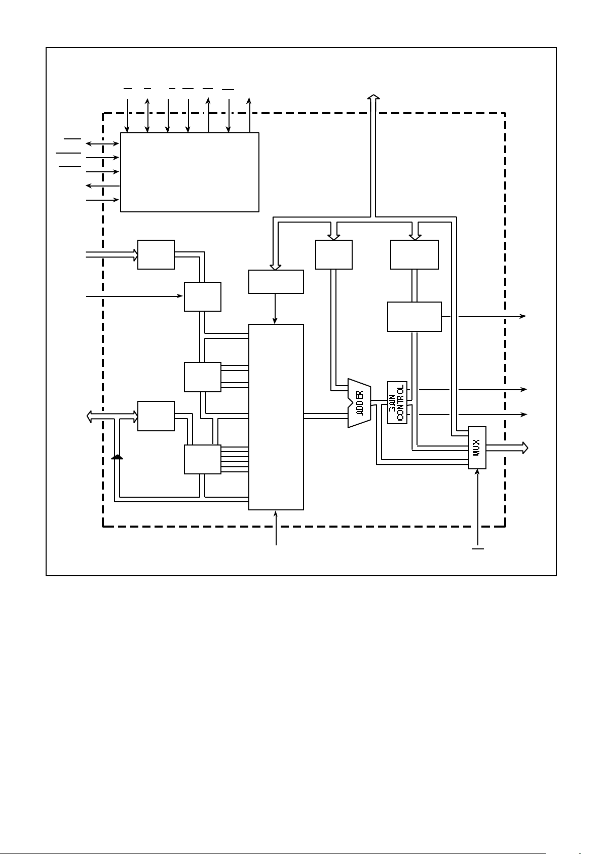
A B C D E F G H J K L M N
1
2
3
4
5
6
7
8
9
10
11
12
13
PIN 1
PIN 132
Fig. 3a Pin connections for 84 I/O pin grid array package - AC84 (Power ) (bottom view)
Fig 3b Pin connections for 132 I/O ceramic power flatpack - GC132 (Power) (top view)
Fig 3 Pin connection diagrams (not to scale). See Table 3 for signal descriptions and Tables 4 and 5 for pinouts.
Page 5
5
Pin
1
2
3
4
5
6
7
8
9
10
11
12
13
14
15
16
17
18
19
20
21
22
23
24
25
26
27
28
29
30
31
32
33
Pin
34
35
36
37
38
39
40
41
42
43
44
45
46
47
48
49
50
51
52
53
54
55
56
57
58
59
60
61
62
63
64
65
66
Signal
N/C
D0
OEN
BIN
PC1
V
DD
GND
OVR
N/C
HRES
R/W
CE
N/C
N/C
GND
N/C
DS
GND
V
DD
PROG
GND
CS3
CS2
CS1
CS0
V
DD
RES
PC0
N/C
DELOP
X0
X1
N/C
Signal
N/C
X2
X3
X4
N/C
X5
GND
X6
X7
N/C
X8
X9
V
DD
V
DD
V
DD
X10
MASTER
N/C
X11
X12
SINGLE
GND
GND
N/C
X13
X14
N/C
X15
V
DD
BYPASS
IP0
V
DD
N/C
Pin
67
68
69
70
71
72
73
74
75
76
77
78
79
80
81
82
83
84
85
86
87
88
89
90
91
92
93
94
95
96
97
98
99
Signal
N/C
IP1
GND
IP2
N/C
V
DD
IP3
V
DD
IP4
GND
IP5
GND
IP6
V
DD
IP7
V
DD
N/C
L7
GND
L6
GND
L5
V
DD
L4
V
DD
L3
V
DD
L2
GND
L1
F1
L0
N/C
Pin
100
101
102
103
104
105
106
107
108
109
110
111
112
113
114
115
116
117
118
119
120
121
122
123
124
125
126
127
128
129
130
131
132
Signal
N/C
V
DD
F0
D15
N/C
D14
D13
GND
D12
GND
V
DD
V
DD
D11
D10
D9
GND
CLK
CLK
CLK
GND
GND
D8
V
DD
D7
D6
D5
D4
GND
D3
N/C
D2
D1
N/C
Table 5 Pin connections for GC132 (power) package. See Fig 3b.
Pin
A1
B1
C2
C1
D2
D1
E2
E1
F2
G2
G1
H2
J1
J2
K1
K2
L1
Signal
L0
F1
L1
L2
L3
N/C
L4
L5
L6
L7
IP7
N/C
IP6
IP5
IP4
N/C
IP3
Pin
L2
M1
N1
N2
M3
N3
M4
N4
M5
N5
M6
M7
N7
M8
N9
M9
N10
Signal
IP2
IP1
IP0
BYPASS
X15
X14
X13
N/C
SINGLE
X12
X11
MASTER
X10
X9
X8
X7
X6
Pin
M10
N11
M11
N12
N13
M13
L12
L13
K12
K13
J12
J13
H12
G12
G13
F12
E13
Signal
X5
X4
X3
X2
X1
X0
DELOP
PC0
RES
CS0
CS1
CS2
CS3
PROG
DS
CE
R/W
Pin
E12
D13
D12
C13
C12
B13
A13
A12
B11
A11
B10
A10
B9
A9
B8
B7
A7
Signal
HRES
OVR
PC1
BIN
OEN
D0
D1
D2
D3
D4
D5
D6
D7
D8
CLK
N/C
D9
Pin
B6
A5
B5
A4
B4
A3
B3
A2
F1
N6
F13
A6
H1
N8
H13
A8
Signal
D10
D11
N/C
D12
D13
D14
D15
F0
V
DD
1
V
DD
2
V
DD
3
V
DD
4
GND1
GND2
GND3
GND4
Table 4 Pin connections for AC84 (power) package. See Fig. 3a.
Page 6

6
BASIC OPERATION
The PDSP16488A convolver performs a weighted sum of all
the pixels within an N3N two dimensional window. Each pixel
value is multiplied by a signed coefficient, or weight, and the
products are summed together. In practice positive weights
would be used to produce averaging effects, with various distribution laws, and negative weights would be used for edge
enhancement. The window is moved continuously over the video
frame, and for real time operation a new result must be obtained
for every pixel clock. In most applications odd sized windows will
be used, resulting in a centre pixel whose value is modified by the
surrounding pixels.
Output Accuracy
With 8 bit pixels, and an 838 window, it is possible for the
accumulated sum to grow to 22 bits within a single device. With
16-bit pixels, and an 834 window (the maximum possible), the
sum can grow to 29 bits. The PDSP16488A actually allows for
word growth up to 32 bits, and thus allows several devices to be
cascaded without any danger of overflow. Since coefficients can
be negative, the final result is a 32-bit signed two’s complement
number.
In a particular application the desired output will lie somewhere within these 32 bits, the actual position being dependent
on the coefficient values used. This causes problems in physically choosing which output pins to connect to the rest of the
system. To overcome this problem the PDSP16488A contains a
gain control block, which allows the final result to be aligned to the
most significant end of the 32-bit internal result. The provision of
the gain control block, rather than a simple shifter, allows the gain
to be defined more accurately.
The sixteen most significant bits of the adjusted result are
available on output pins D15:0, which contains a sign bit.
Output Saturation
If the output from the convolver is driving a display, negative
pixels will give erroneous results. An option is thus provided
(register bits C7:6) that forces all negative results to zero, which
are then interpreted as black by the display. At the same time
positive results, which overflow the gain control, are forced to
saturate at the most positive number, i.e. peak white. In this mode
the output sign bit is always zero,and should not be connected to
an A-D converter.
A separate option forces both negative and positive overflows
to saturate at their respective maximum values, but in scale
negative results remain valid. A gain control overflow warning flag
(OVR) is also available, which can be used in a host CPU
supported system to change the gain parameters if overflows are
not acceptable.
Binary Output
The PDSP16488A contains a 16-bit arithmetic comparator
which allows the output from the gain control block to be compared with a previously programmed value. An output flag allows
the user to detemine if the result was above or below a value
contained within an internal register.
Multiplier Array
The PDSP16488A contains sixteen 838 multipliers each
producing a 16-bit result. Internally the pixel clock supplied by
the user can be multiplied by two or four, which together with
the proprietary architecture, allows each multiplier to be used
several times within a pixel clock period. This increases the
effective number of multipliers, which are available to the user,
from 16 to 32 or 64 respectively. This architecture produces a
very efficient utilization of chip area, and allows the line delays
to be accommodated on the same device.
The sixteen multipliers are arranged in a 4 deep by 4 wide
array, resulting in effective arrays of 4 by 8 or 8 by 8 with the multicycling options. The multiplier array can also be configured to
handle 16-bit signed pixels; the effective number of available
multipliers is then halved.
Line Delay Operation
Internal RAM is arranged in two separate groups, and can be
configured to provide line delays to match the chosen size of the
convolver. When a four deep arrangement is used, with 8-bit
pixels, four line delays are available, and each can be programmed to contain up to 1024 pixels. In an eight deep array,
or if 16-bit pixels are needed, each line can contain up to 512
pixels. Fig. 4 illustrates the options available.
The first line delay in one of the groups can optionally be
switched in or out under the control of an input pin. It is used to
delay the pixel input when data is obtained from another
convolver in a multiple device system, or it is used to support
interlaced video.
Signals L7:0 may be used as pixel inputs or outputs. They
are configured as inputs at power-on to avoid possible bus
conflicts, but by setting a mode control bit can become outputs.
They can then be used to drive another device when multiple
PDSP16488As are required.
Interlaced Video
When using real time interlaced video, a picture or frame is
composed from two fields, with odd lines in one field and even
lines in the other. An external field delay is thus required to gather
information from adjacent lines, and the convolver needs two
input buses. The bus providing the delayed pixels has an extra
internal line delay. This is only used in the field containing the
upper line in any pair of lines, and must be bypassed in the other
field. It ensures that data from the previous field always corresponds to the line above the present active line, and avoids the
need to change the position of the coefficients from one field to
the next.
Fig. 5 shows the translation from physical to internal line
positions, for single device interlaced systems. Line N is the line
presently being convolved, which is either one or two lines
previous to the line presently being produced.
When windows requiring four or more lines are to be implemented, the first line delay, in the group supplied from the L7:0
pins, must always be bypassed. This bypass option is controlled
by register B, bit 7 and is not effected by the BYPASS input pin..
The coefficients must be loaded into the locations shown, which
match the translated line positions, with unused coefficients,
shown shaded, loaded with zeros.
Defining the Length of the Line Delay
Fig. 5 defines the maximum line lengths available in each of
the window size options. The actual line lengths can be defined
in one of three ways, to support both real time applications, taking
pixels directly from a camera, and also use in systems supported
by a frame store. In the former case the line delays must be
referenced to video synchronization pulses. In the latter case the
line lengths are well defined, and the horizontal flyback ‘dead
times’ will have been removed.
Page 7
7
Fig. 4 Line delay configurations
512
512
512
512
838
ARRAY
512
512
512
512
IP7:0
BYPASS
L7:0
BYPASS
512
512
512
512
838
ARRAY
512
512
512
512
IP7:0
BYPASS
L7:0
BYPASS
1024
1024
1024
1024
434
OR
834
ARRAY
IP7:0
BYPASS
L7:0
1024
1024
1024
1024
434
OR
834
ARRAY
IP7:0
BYPASS
L7:0
512
512
512
512
512
512
512
512
IP7:0
BYPASS
L7:0
BYPASS
434
OR
834
ARRAY
16
16
16
16
To support real time applications an option is provided in
which the length of the line delay is defined by the number of
clocks obtained while the HRES input is low. HRES would
normally be composite sync when the convolver is directly
attached to an NTSC or PAL video input.
The line delay is achieved by reading the previous contents
of a RAM-based line store, and then writing new information to
the same address. When HRES is high, write operations are
inhibited, and the address counter is reset. During an active line
the counter is incremented by the pixel clock. If the maximum
count is reached before the end of a line, then write operations are
terminated and wraparound effects avoided.
The rising edge of HRES, marking the end of a line, is
normally asynchronous to the pixel clock, and it is possible for an
additional pixel to be stored on some lines. This has no effect on
the convolver operation, and will not cause a cumulative shift in
the pixel position from line to line.
An alternative means of defining the line length is, however,
provided when an exact number of pixels is needed. HRES going
low then starts the delay operation for every line, but it ceases
when the 10-bit value contained in two registers is reached. This
method can avoid the need to store blank pixels at the end of a
line before HRES goes high. With this method the line must
contain an even number of pixels but the value loaded into the
control registers, defining the line length, must be one less than
the even number required.
In an image processing system, the pixel clock is often resynchronized, or even inhibited, during blanking or sync. The
next line is then started with a precise time interval from the end
of sync (falling edge of HRES) to the first pixel clock edge. This
avoids any visible pixel jitter at the beginning of the line, which
would otherwise be present since pixel clock is asynchronous
with respect to video sync pulses.
When using the PDSP16488A the pixel clock should not be
inhibited, or re-synchronized, until the delayed version of the
HRES input goes active. This is present on the DELOP output
pin. This will ensure that no pixels on the right hand edge are lost
due to the internal pipeline delay. If the pixel clock is a continuous
signal, the user must ensure that the HRES high to low transition
meets the timing requirements defined in Fig. 10. The HRES
rising edge at the end of a line need not be synchronized.
When pixels are read or written to a frame store, an alternative
line delay configuration is needed. Within the frame store lines
would be stored in contiguous locations, with no gaps caused by
the flyback period between the lines. This method of use makes
the HRES defined line delay operation difficult to use, and an
alternative mode of operation is provided. The HRES input is then
driven by a system-provided signal, which defines a complete
frame store update period. It is not a line defining signal. The high
to low transition of this signal will initiate the line store update
sequence and allow the internal address pointers to increment.
These pointers will be synchronously reset at the end of a line,
when they reach the pre-programmed value. They will then
immediately start a new operation using address zero. The actual
line delay must be pre-loaded into two control registers as
described previously.
Write operations back to the frame store must allow for the
total pipeline delay. This can be achieved by inhibiting write
operations until DELOP goes low. Write operations then continue
until it goes back high. The PDSP16488A assumes that data is
valid when a clock signal is applied, and that it also meets the set
up and hold requirements given in Fig. 10. If data is not valid due,
for example, to a frame store DRAM refresh cycle, then the user
must externally inhibit the clock. The clock supplied to the
convolver will in this mode be a signal which defines a frame store
cycle time.
The use of the convolver in a line scan system is similar to its
use with a frame store. These systems have no flyback period,
and the address counter must be synchronously reset at the end
of the line and then allowed to continue.
Page 8
8
1024
1024
1024
1024
434
OR
834
ARRAY
IP7:0
ODD
FIELD
Output is shifted
by 1 line in
every field
FIELD
DELAY
VIDEO
LINE N12
L7:0
N11
N21
N
L7:0
512
512
512
512
838
ARRAY
512
512
512
512
IP7:0
FIELD
DELAY
Output is shifted
by 1 line in
every field
ODD
FIELD
DELAY
BYPASSED
REG B BIT 7 SET
VIDEO
LINE N12
N11
N21
N12
N
N22
L7:0
512
512
512
512
838
ARRAY
512
512
512
512
IP7:0
FIELD
DELAY
Output is shifted
by 2 lines in
every field
ODD
FIELD
DELAY
BYPASSED
REG B BIT 7 SET
VIDEO
LINE N14
N13
N11
N14
N
N22
N21
N23
N12
C24
C56
C16
C48
C8
C40
C0
C32
LINE N23
LINE N22
LINE N21
LINE N
LINE N11
LINE N12
LINE N13
LINE N14
C25
C57
C17
C49
C9
C41
C1
C33
C26
C58
C18
C50
C10
C42
C2
C34
C27
C59
C19
C51
C11
C43
C3
C35
C28
C60
C20
C52
C12
C44
C4
C36
C29
C61
C21
C53
C13
C45
C5
C37
C30
C62
C22
C54
C14
C46
C6
C38
C31
C63
C23
C55
C15
C47
C7
C39
838 WINDOW
C48
C8
C40
C0
C32
LINE N22
LINE N21
LINE N
LINE N11
LINE N12
C49
C9
C41
C1
C33
C50
C10
C42
C2
C34
C51
C11
C43
C3
C35
C52
C12
C44
C4
C36
535 WINDOW
C4
C8
C0
LINE N21
LINE N
LINE N11
C5
C9
C1
C6
C10
C2
333 WINDOW
Fig. 5 Line delay allocations in SINGLE device interlaced systems
Page 9
9
Gain Control Block
This block is provided as an aid to locating the bits of interest
in the 32-bit internal result. The magnitude of the largest convolved
output will depend on the size of the window, and the coefficient
values used. The function of the gain control block is then to
produce an output, which is accurate to 16 bits, and which is
aligned to the most significant end of this 32-bit word. The sixteen
most significant bits of the word are available on D15:0 and the
largest number need only have one sign bit if the gain control is
correctly adjusted.
Fig. 6 indicates the mechanism employed with the required
function implemented in two steps. Two mode control bits,
register C, bits 5:4, allow one of four 20 bit fields to be selected
from the final 32-bit value. These four fields are positioned with
the first at the most significant end, and then at four bit
displacements down to the least significant end.
By setting an enabling bit, register C, bit 0, the field selection
can optionally be done automatically. This feature should only be
used in the real time operating mode, when HRES defines video
lines. Internal logic examines the most significant 13, 9, or 5 bits
from the 32-bit result, and makes a field selection dependent on
which group does not contain identical sign bits. If less than five
sign bits are obtained, the logic will select the field containing the
most significant 20 bits. The selection is indicated by F1:0.
The automatic field selection is particularly useful when a
fixed scene is being processed. The selection is reset when any
internal register is updated (i.e.
PROG
has been low) and is then
held high for ten further occurrences of the HRES input. This
allows the internal multiplier/accumulator array to be completely
flushed before a field selection is made. As convolver outputs of
greater magnitude are produced the field selection logic will
respond by selecting a more significant field. The most significant
field found necessary remains selected until
PROG
again goes
low. Even if the automatic field selection is not enabled, F1:0 will
still indicate which field would have been selected. These are
coded in the same way as register C, bits 5:4.
Having chosen a field, either manually or automatically, it
is then multiplied by a 4-bit unsigned integer. This is contained
within the user-programmed gain control register, and the
multiplication will produce a 24-bit result . The middle 16 bits
of this result contain the required output bits. The gain control
multiplier can overflow in to the unused most significant four
bits if the parameters are chosen wrongly. This condition is
flagged by pin OVR.
By setting appropriate mode control bits, further manipulation
of the gain control output is possible. One option, register C, bits
Fig. 6 Gain control block
7:6 = 11, allows all negative outputs to be forced to zero, and at
the same time positive gain control overflows will saturate at the
maximum positive number. Register C, bits 7:6 = 10 will saturate
positive and negative overflows at their respective maximum
values, but otherwise leaves them unchanged. Occasional overflows can be tolerated in some systems, and this option prevents
any gross errors.
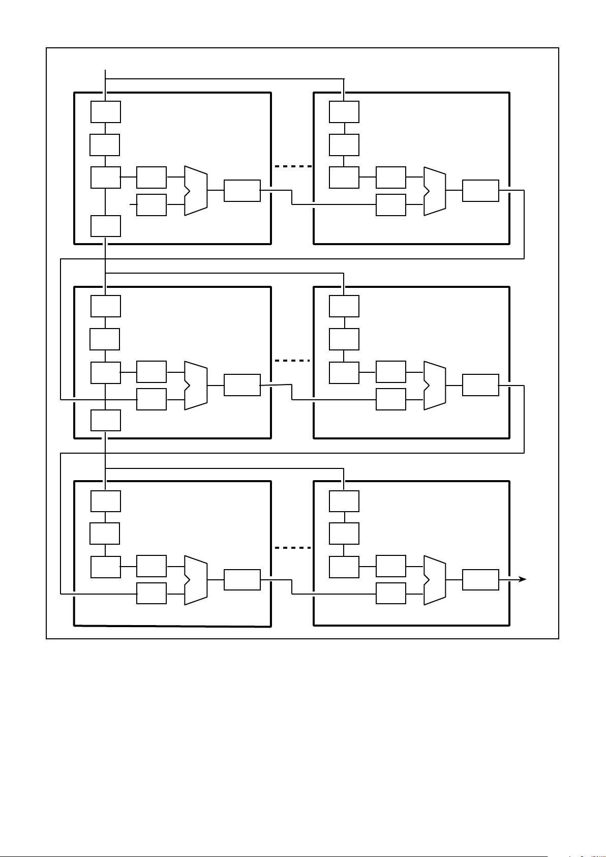
Expansion
Multiple devices can be connected in cascade in order to
obtain window sizes larger than those provided by a single
PDSP16488A. This requires an additional adder in each device
which is fed from expansion data inputs. This adder is not used
by a Single device or the first device in a cascaded system, and
is enabled or disabled by register B, bit 4.
The first device in the cascaded system must be designated
as a Master device by
MASTER
tying low. Its expansion input
bus is then used as the source of data for the coefficient and
control registers in all devices in the system.
In order to reduce the pin count required for 32-bit buses, both
expansion in and data out are time-multiplexed with the phases
of the pixel clock. When the clock is high the least significant half
will be valid, and when the clock is low the most significant half will
be valid.
In practice this multiplexing is only possible with pixel clocks
up to 20MHz. Above these frequencies the multiplexing must be
inhibited by setting register A, bit 7. The intermediate data
accuracy will then be reduced, since only the lower 16 bits of the
internal 32-bit intermediate sum are available on the D15:0 output
pins. In such systems the coefficients must be scaled down in
order to keep the intermediate and final results down to 16 bits.
The final device should not use the gain control block but instead
should simply output the non-multiplexed 16-bit result. The OVR
flag and pixel saturation options will not be available.
Pixel Input and Output Delays
In a real time system, when line delays are referenced to
video sync pulses present on the HRES input, the first pixel from
the last line delay does not appear on the L7:0 pins until the fifth
active pixel clock edge after HRES has gone low. This is
illustrated in Fig. 8. In a vertically expanded system, this output
provides the input to the first line delays in the vertically displaced
devices. The internal logic is thus designed to always expect this
five clock delay. Compensation must thus be applied to the
devices which are directly connected to the video source, such
that the first pixel is not valid until the fifth clock rising edge.
For this reason the PDSP16488A contains an optional four
clock pipeline delay on each of the pixel data inputs, as shown in
Fig. 7. When the delay is used the first pixel in a video line must
be available on the input pins after the first pixel clock edge. This
would be so if the device were connected to an A-D converter,
since that would introduce a one pixel pipeline delay. If the system
introduces any further external pipeline delays, then the internal
delay should be bypassed, and the user should ensure that the
first pixel is valid after the fifth clock edge.
The use of this four clock delay is controlled by register B,
bit 3. This delay is in addition to the delays which are provided to
support expansion in both the X and Y directions, and are
controlled by register D, bits 3:2. Both delays are in fact simply
added together in the device, but are separately defined since
they add delays for different system reasons.
FROM EXPANSION ADDER
AUTOMATIC
FIELD SELECT
32 BITS
204 8 208 4 201220 12
MUX
GAIN CONTROL
REGISTER
4
16
4
20
4
24
SATURATE
LOGIC
16
MSB
LSB
D15:0
F1:0
Page 10
10
4 CLOCK
DELAY
LINE
DELAYS
0
DELAYS
Σ
WIDTH = S
+
4 CLOCK
DELAYS
0
DELAYS
0
DELAYS
ZERO
REG B3 = 1
DELAY = 0, DEFINED BY REG D3:2 = 00
REG D0 = 0
4 CLOCK
DELAY
LINE
DELAYS
0
DELAYS
Σ
WIDTH = S
+
4 CLOCK
DELAYS
D
DELAYS
0
DELAYS
REG B3 = 0
D = 41S(N21) DEFINED BY REG D3:2
REG D0 = 0
4 CLOCK
DELAY
LINE
DELAYS
0
DELAYS
Σ
WIDTH = S
+
D
DELAYS
0
DELAYS
4 CLOCK
DELAY
LINE
DELAYS
0/4
DELAYS
Σ
WIDTH = S
+
0
DELAYS
0
DELAYS
REG D0 = 0 IF S = 4,
OR REG D0 = 1 IF S = 8
Nth PDSP16488A IN THE ROW
4 CLOCK
DELAY
LINE
DELAYS
0/4
DELAYS
Σ
WIDTH = S
+
D
DELAYS
0
DELAYS
Nth PDSP16488A IN THE ROW
4 CLOCK
DELAY
LINE
DELAYS
0/4
DELAYS
Σ
WIDTH = S
+
D
DELAYS
0
DELAYS
REG B3 = 1
D = 41S(N21) DEFINED BY REG D3:2
Nth PDSP16488A IN THE ROW
INPUT
OUTPUT
PDSP16488A
PDSP16488A
PDSP16488A
REG B3 = 1
DELAY = 0, DEFINED BY REG D3:2 = 00
REG D0 = 0 IF S = 4,
OR REG D0 = 1 IF S = 8
REG B3 = 1
D = 41S(N21) DEFINED BY REG D3:2
REG D0 = 0 IF S = 4,
OR REG D0 = 1 IF S = 8
REG B3 = 0
D = 41S(N21) DEFINED BY REG D3:2
REG D0 = 0
Fig. 7 Multi-device delay paths
Delay Compensation for Large Windows
A large window is composed of several partial windows each of
which is implemented in an individual device. If necessary the partial
window must be padded with zero coefficients to become one of the
standard sizes. When constructing a large window it is necessary to
delay the expansion data inputs in order to compensate for growth
in the horizontal direction. Delays in the partial sums are also
necessary to compensate for the total pipeline delay needed to
produce the previous complete horizontal stripe.
Within each device in a horizontal stripe, apart from the first,
the expansion input must be delayed by the width of the partial
window, before it is added to the internal sum. Since partial
windows can only be 4 or 8 pixels wide, a delay of 4 or 8 pixel
clocks is needed. There is, however, an in-built delay of 4 pixels
in the inter device connection, and the PDSP16488A thus only
needs an option to delay the expansion input by an additional four
pixels.
Page 11

11
The data from the last device in a horizontal row of convolvers
feeds the expansion input of the first device in the next row. This
is shown in Fig. 7. With this arrangement, the position of the partial
window as illustrated, is the inverse of its vertical position on a
normal TV screen. Thus the top left hand device corresponds to
the bottom left hand portion of the complete window.
The output from the last device in the row is delayed with
respect to the original data input by an amount given by the
formula;
DELAY = 41S(N21), where N is the number of devices in a
row and S is the partial window width, i.e. 4 or 8.
The internal convolver sums, in each of the devices in the next
row, must be delayed by this amount before they are added to
results from the previous row. This is more conveniently achieved
by delaying data going into the line stores. The required cumulative delay with respect to the first horizontal stripe is then
automatically obtained when more than two rows of devices are
needed.
Register D, bits 3:2 are used to define one of four delay
options. These delays have been selected to support systems
needing from two to eight devices and are described in the
applications section.
Coefficients
Sixty-four coefficients are stored internally and must be
initially loaded from an external source. Table 5 gives the
coefficient addresses within a device, with coefficient C0 specified by the least significant address and C63 by the most
significant address. Fig. 9 shows the physical window position
within the device that is allocated to each coefficient in the various
modes of operation. Horizontally the coefficient positions correspond to the convolution process as if it were observed on a
viewing screen, i.e. the left hand pixel is multiplied with C0. In the
vertical direction the lines of coefficients are inverted with respect
to a visual screen, i.e. the line starting with C0 is actually at the
bottom of the visualized window.
The coefficients may be provided from a Host CPU using
conventional addressing, a read/not write line, data strobe, and
a chip enable. Alternatively, in stand alone systems, an EPROM
may be used. A single EPROM can support up to 16 devices with
no additional hardware.
When windows are to be fabricated which are smaller than
the maximum size that the device will provide in the required
configuration, then the areas which are not to be used must
contain zero coefficients. The pipeline delay will then be that of a
completely filled window.
Function
Mode Reg A
Mode Reg B
Mode Reg C
Mode Reg D
Comparator LSB
Comparator MSB
Scale value
Pixels/line LSB
Pixels/line MSB
C0-C15
C16-C31
C32-C47
C48-C63
Unused
Hex address
00
01
02
03
04
05
06
07
08
40-4F
50-5F
60-6F
70-7F
09-3F
Table 5 Internal register addressing
Data size
8
8
8
15
16
Window size
434
834
838
434
834
Pipeline delay
34
30
26
28
26
Table 6 Pipeline delays
Total Pipeline Delay
The total pipeline delay is dependent on the device configuration and the number of devices in the system. Table 6 gives the
delays obtained with the various single device configurations
when the gain control is used. These delays are the internal
processing delays and do not include the delays needed to move
a given size window completely into a field of interest. When
multiple devices are needed, additional delays are produced
which must be calculated for the particular application. These
delays are discussed in the applications section.
The PDSP16488A contains facilities for outputting a delayed
version of HRES (DELOP) to match any processing delay.
Register C. bits 3:1 allow this delay to be selected from any value
between 29 and 92 pixel clocks as detailed in Table 9.
CLK
t
RSU
HRES
(sync)
ACTIVE LINE PERIOD
2 3 4 5 6 7 8 1 2 6 7
FIRST
PIXEL
VALID
(REG B3
SET)
FIRST
PIXEL
FROM
LINE
STORE
VALID
LAST2
PIXELS
INTER-
NALLY
STORED
ASYNCHRONOUS BACK EDGE
LINE STORE
WRITES INHIBITED
Fig.8 Pixel input delays
Page 12

12
Fig. 9 Physical coefficient positions
C0
C8
C16
C24
C32
C40
C48
C56
C1
C9
C17
C25
C33
C41
C49
C57
C2
C10
C18
C26
C34
C42
C50
C58
C3
C11
C19
C27
C35
C43
C51
C59
C4
C12
C20
C28
C36
C44
C52
C60
C5
C13
C21
C29
C37
C45
C53
C61
C6
C14
C22
C30
C38
C46
C54
C62
C7
C15
C23
C31
C39
C47
C55
C63
838, 8-BIT DATA
512
512
512
L7:0
512
512
512
512
IP7:0
512
C0
C32
C8
C40
16
C16
C48
C24
C56
C1
C33
C9
C41
C17
C49
C25
C57
C2
C34
C10
C42
C18
C50
C26
C58
C3
C35
C11
C43
C19
C51
C27
C59
C4
C36
C12
C44
C20
C52
C28
C60
C5
C37
C13
C45
C21
C53
C29
C61
C6
C38
C14
C46
C22
C54
C30
C62
C7
C39
C15
C47
C23
C55
C31
C63
834, 16-BIT DATA
512
512
512
512
L7:0
512
512
512
512
IP7:0
LSB
16
16
16
MSB
C0
C8
C16
C24
C1
C9
C17
C25
C2
C10
C18
C26
C3
C11
C19
C27
C4
C12
C20
C28
C5
C13
C21
C29
C6
C14
C22
C30
C7
C15
C23
C31
834, 8-BIT DATA
L7:0
1024
1024
1024
1024
IP7:0
C0
C4
C8
C12
C1
C5
C9
C13
C2
C6
C10
C14
C3
C7
C11
C15
434, 8-BIT DATA
L7:0
1024
1024
1024
1024
IP7:0
C0
C16
C4
C20
16
C8
C24
C12
C28
C1
C17
C5
C21
C9
C25
C13
C29
C2
C18
C6
C22
C10
C26
C14
C30
C3
C19
C7
C23
C11
C27
C15
C31
434, 16-BIT DATA
512
512
512
512
L7:0
512
512
512
512
IP7:0
LSB
16
16
16
MSB
NOTE: Two coefficients occurring in the same box have identical values
Page 13

13
Loading Registers from a Host CPU
The X14:0 expansion data inputs on a single or master device
are connected to the host bus to provide address and data for the
internal registers. In a multiple device system the remaining
devices receive addresses and data which have been passed
through the expansion connection between earlier devices in the
cascade chain. Each device needs an individual chip enable
(CE) plus a global data strobe (DS), a read/ not write (
R/W
) line,
and
PROG
signal from the host.
Registers are individually addressed and can be loaded in any
sequence once the global
PROG
signal has been produced by the
host. The latter would normally be produced from an address decoder
encompassing all the necessary device addresses.
If a self-timed system is to be implemented, a timing strobe
must be passed down the expansion chain through
the
PC0/PC1
connections. The
PC0
output from the final device
is used as a host
REPLY
signal, and indicates that the last
device has received data after the propagation delay of previous
devices. The timing strobe is produced in the Master device from
the host data strobe, and will appear on the
PC0
output. This
feature allows the user to cascade any number of devices without
having to know the propagation delay through each device. The
timing information for this mode of operation is given in Fig. 10.
The host can also read the data contained in the internal registers.
The required device is selected using chip enable with the
R/W
line
high, indicating a read operation. Single device systems output the
data read on X7:0, but in multiple device systems data is read from
the D7:0 outputs on the final device in the chain. These must be
connected back to the host data bus through tristate drivers, whose
tristate control must be generated externally (see Figs. 14 and 15).
When earlier devices in the chain are addressed, the register
contents are transferred through the expansion connections down to
the final device. In the self timed configuration the data will be valid
when
REPLY
is taken low by
PC1
, as shown in Fig. 10.
If
REPLY
is not to be used, the
PC0/PC1
connections are
not necessary, and the host data strobe for a write operation must
be wide enough to allow for the worst case propagation delay
through all the devices (t
DEL
). If the data or address from the host
does not meet the set up time given in Fig. 8, the width of the data
strobe can be simply extended to compensate for the additional
delay. When reading data the access time required is
t
ACC1tDEL
(N21), using the maximum times given in the Host
Mode Switching Characteristics.
Host control lines
X7:0 8-bit data bus. In a Single device system this bus is
bidirectional; in other configurations it is an input.
Only a Single or Master device is connected directly
to the host. Other devices receive data from the
output of the previous device in the chain.
X14:8 7-bit address bus which is used to identify one of the
73 internal registers. Connected in the same manner as X7:0.
X15 X15 must be open circuit on the Master device
An input from the previous
PC1
output in a multiple
device chain. Not needed on a Single device or if the
self timed feature is not used.
Reply to the host from a Single device or from the
last device in a cascade chain. It indicates that the
write strobe can be terminated. Connected to
PC0
input of the next device at intermediate points in the
chain if the self timed feature is used.
PROG
DS
CE
R/W
Read/Not Write line from the host CPU which is
connected to all devices in the system.
An active low enable which is normally produced
from a global address decode for the particular
device. This must encompass all internal register
addresses.
An active low host data strobe which is connected to
all devices in the system.
An active low global signal, produced by the host,
which is connected to all devices in the system.
Together with a unique chip enable for every device,
it allows the internal registers to be updated or
examined by the host
PROG
andCEshould be tied
together in a Single device system.
Loading Registers from an EPROM
In the EPROM mode, one device has to assume the role of
a host computer. If more than one device is present, this must be
the first component in the chain, which must have its
MASTER
pin tied low.
The Master device contains internal address counters which
allow the registers in up to 16 cascaded PDSP16488As to be
specified. It also generates the
PROG
signal and a data strobe
on the pins which were previously inputs. These outputs must be
connected to the other devices in the system, which still use them
as inputs. The
R/W
input should be tied low on all devices.
The width of the data strobe is determined by the feedback
connection from the
PC1
output on the last device to the
PC0
input
on the Master. The
PC0/PC1
connections must be made between devices in a multiple device system; in a single device
system the connection is made internally.
The available EPROM access time is determined by an
internal oscillator and does not require the pixel clock to be
present during the programming sequence. Any pixel clock resynchronization in a real time system will thus not affect the
coefficient load operation. The relevant EPROM timing information is shown in Fig. 11.
The load procedure will commence after
RES
has gone from
low to high, and will be indicated by the
PROG
output going
low. The data from 73 EPROM locations will be loaded into the
internal registers using addresses corresponding to those in
Table 5. Within a particular page of 128 EPROM locations, the
first nine locations supply control register information, and the
top 64 supply coefficients. The middle 55 locations are not
used. If the window size is 834, the top 32 locations will also
contain redundant data, and if the size is 434 the top 48 will
be redundant.
In a multiple device system the load sequence will be repeated for every device, and four additional address bits will be
generated on the CS3:0 pins. These address bits provide the
EPROM with a page address, with one page allocated to each
device in the system. Within each page only 73 locations provide
data for a convolver, the remainder are redundant as in the single
device system. The CS3:0 outputs must also be decoded in order
to provide individual chip enables for each device. These can
readily be derived by using an AS138 TTL decoder. Bits in an
internal control register determine the number of times that the
sequence is repeated.
If changes to the convolver operation are to be made after
power-on, activating theCEinput on the Master or Single
device will instigate the load procedure. Additional EPROM
address bits supplied from the system will allow different filter
coefficients to be used.
PC0
PC1
Page 14

14
R/W
DS
cease when the value in the counter equals that
contained in these bits. The bits are redundant in a
Single device which only uses one 128-byte block.
BITS 6:4 These bits define one of the five basic configurations.
The line delays will automatically be configured to
match the chosen window size and pixel accuracy.
The maximum clock rate that is available to the user
reflects the internal multiplication factor.
BIT 7 This bit must be set if the pixel clock is greater than
20MHz. It disables the output and input time
multiplexing, and instead outputs the least significant
half of the 32-bit intermediate sum for the complete
clock cycle. When the gain control is used, the output
multiplexing will automatically be disabled.
Register B bit allocation (Table 9)
BIT 0 This bit defines the input for the second group of line
delays. It must be set in the 16-bit pixel modes, and
is set by power on reset.
BIT 2:1 These bits control the mode of operation of the line
stores. In real time systems pixels can be stored
either until HRES (sync) goes high , or until a predetermined count is reached. In the frame store
mode line store operations are continuous, with a
pre-determined line length.
BIT 3 When this bit is set four pipeline delays are added to
the pixel inputs to compensate for the internal/
external delays between line stores. The extra delay
is only necessary when a device supplied with
system video in which the first pixel in a line is valid
in the period following the first active clock edge. See
Fig 7. The delay is not necessary if the device is fed
from the output of another convolver. When set this
bit will add four additional delays to those defined by
register D, bits 4: 2.
BIT 4 When this bit is set the expansion adder will not be
used. It is automatically set in a Master or Single
device.
EPROM control lines
X7:0 8 bit data from the EPROM to the Master or Single
device. Otherwise data is received from the previous
device in the chain.
X14:8 Lower 7 address bits to the EPROM from a Master or
Single device. Otherwise an input from the data
output of the previous device.
X15 Tied to ground on a Master device to indicate the
EPROM mode.
Tied low on all devices.
An output from a Master or Single device which
provides a data strobe for the other devices. A pullup
resistor is required on this pin in EPROM mode
CS3: 0 Four additional address bits for the EPROM which are
provided by the Master device. They allow 16 additional devices to be used and must be externally
decoded to provide chip enables.
An input on the Master device which is driven from
the
PC1
output of the last device in the chain. Used
internally to terminate the write strobe. Connected
to previous
PC1
outputs at intermediate points in
the chain. Not needed for a Single device.
An output connected to the
PC0
input of the next
device in the chain. The last device feeds back to the
Master. Not needed for a Single device.
An enable which is produced by decoding CS3:0 from
the Master. It is not needed for a Master or Single
device which will always use the bottom block of
addresses with internally generated write strobes. It
can, however, be used on these devices to initiate a
new load procedure after the initial power-on
sequence.
An active low signal produced by an EPROM supported Master or Single device. An input to all other
devices. It indicates that a register load sequence
is occurring, either after power on, or as the result
ofCE as explained above. It remains active until
register 73 in the final device has been loaded.
Register A, bits 3:0 define the number of cascaded
devices. A pullup resistor is required on this pin in
EPROM mode.
System Configuration
The device is configured using a combination of the state of
the
SINGLE
and
MASTER
pins, and the contents of the four
Mode Control registers. In a Master or Single device the state of
the X15 pin is used to define whether the system is EPROM or
Host supported, as described above.
Mode Control Registers
Register A bit allocation (Table 8)
BITS 3:0 These bits are ‘don’t care’ when using a host compu-
ter but to a Master device, in an EPROM supported
system, they define the number of interconnected
chips. The EPROM must contain contiguous 128 byte
blocks for each of the devices in the system and a 4bit counter in the Master device will sequence through
up to 16 block reads. An internal comparator in the
Master causes the loading of the internal registers to
PC0
PC1
CE
PROG
Function
Number of extra devices from 1-15
8-bit, 838 window, 10MHz max.,
83512 line delays.
16-bit, 834 window, 10MHz max.,
43512 line delays.
16-bit, 434 window, 20MHz max.,
43512 line delays.
8-bit, 834 window, 20MHz max.,
431024 line delays.
8-bit, 434 window, 40MHz max.,
431024 line delays
Multiplexed exp. data
Non-multiplexed exp. data
Code
XXXX
000
001
010
011
101
0
1
Bit
3:0
6:4
6:4
6:4
6:4
6:4
7
7
Table 8 Register A bit functions
Page 15

15
BIT 7 This bit controls the bypass option on the first line
delay on the L7:0 inputs. It is only effective when an
8 bit pixel mode is selected, which also needs more
than four line delays. When L7:0 are used as outputs
it should always be reset. In the 16-bit modes the
bypass function is only controlled by the BYPASS pin,
and the bit is redundant.
Function
Second line delay group fed from the
first group
Second line delay group fed from L7:0
which become inputs
Store pixels to end of line
Store pixels till count is reached
Frame store operation
Not Used
No delays on pixel inputs
4 delays on both pixel inputs
Use expansion adder
Expansion adder disabled
Not used
Use first delay in second group
Bypass first delay in second group
Bit
0
0
2:1
2:1
2:1
2:1
3
3
4
4
6:5
7
7
Code
0
1
00
01
10
11
0
1
0
1
0
1
Register C bit allocation (Table 10)
BIT 0 If this bit is set, the 20-bit field selected from the 32-bit
result, is defined automatically by internal logic.
BITS 3:1 These bits are in conjunction with register D, bits 7:5
to define the pixel delay from the HRES input to the
DELOP output. They are used to match the appropriate processing delay in a particular system. The
minimum delay is 29 pixel clocks.
BITS 5:4 These bits define which of the four 20-bit fields out of
the 32-bit final result is selected as the input to the gain
control. They are redundant when the gain control is
not used, or if register C, bit 0, is set.
BITS 7:6 These bits define the use of the gain control as given
in Table 10. Intermediate devices in a multiple device
system must bypass the gain control block, otherwise
the additional pipeline delays will affect the result.
Disabling the gain control block will reduce the device
pipeline by 13 CLK cycles from the delays shown in
Table 6.
Table 9 Register B bit functions
Table 10 Register C bit functions (continues…)
Function
Field selection defined by C5:4
Automatic field selection
DELOP = 2910 clocks
DELOP = 2918 clocks
DELOP = 29116 clocks
Code
0
1
000
001
010
Bit
0
0
3:1
3:1
3:1
Function
DELOP = 29124 clocks
DELOP = 29132 clocks
DELOP = 29140 clocks
DELOP = 29148 clocks
DELOP = 29156 clocks
Select upper 20 bits
Select next 20 bits
Select next 20 bits
Select bottom 20 bits
By-pass the gain control
Normal gain control output
Saturate at max.1ve and 2ve values.
Force 2ve to zero.Sat.1ve values.
Code
011
100
101
110
111
00
01
10
11
00
01
10
11
Bit
3:1
3:1
3:1
3:1
3:1
5:4
5:4
5:4
5:4
7:6
7:6
7:6
7:6
Table 10 Register C bit functions (continued)
Table 11 Register D bit functions
Register D bit allocation (Table 11)
BIT 0 If this bit is set the expansion data input is delayed
by four pixel clocks before it is added to the present
convolver output. It is used in multiple device systems
when the partial window width is 8 pixels.
BIT 1 When this bit is set the internal sum is shifted to the
left by 8 places before being added to the expansion
input. It is used when two devices are used, each in an
8-bit pixel mode, to construct a 16-bit pixel mode.
BITS 3:2 These bits define the delays on both sets of pixel
inputs before entering the line stores. The delays are
always identical on both sets.
BIT 4 When this bit is set the convolver interprets 8 or 16-
bit pixels as 2’s complement signed numbers
BIT 7:5 These bits add 0 to 7 additional clock delays to those
selected by Register C, bits 3:1.
Function
X15:0 Not delayed
X15:0 Delayed
Internal sum not shifted
Internal sum multiplied by 256
Input to line stores not delayed
Input to line stores delayed by 4
Input to line stores delayed by 8
Input to line stores delayed by 12
Unsigned pixel data input
2’s complement pixel data input
Add 0 to 7 clock delays to DELOP
Bit
0
0
1
1
3:2
3:2
3:2
3:2
4
4
7:5
Code
0
1
0
1
00
01
10
11
0
1
XXX
Page 16

16
ELECTRICAL CHARACTERISTICS
The Electrical Characteristics are guaranteed over the following range of operating conditions, unless otherwise stated:
VDD = 15V±10%, GND = 0V, T
AMB
(Commercial) = 0°C to170°C, T
AMB
(Industrial) = 240°C to 185°C,
T
AMB
(Military) = 255°C to 1125°C
Static Characteristics
Output high voltage
Output low voltage
Input high voltage
Input low voltage
Input leakage current
Input capacitance
Output leakage current
Output short circuit current
Current at full speed
IOH = 4mA
IOL = 28mA
GND < VIN < VDD, no internal pullup
GND < V
OUT
< VDD, no internal pullup
VDD = 15·5V
Conditions
Characteristic
Min. Typ. Max.
10
-
0·4
-
0·8
110
150
300
Max.
2·4
-
2·0
-
210
250
10
V
OH
V
OL
V
IH
V
IL
I
IN
C
IN
I
OZ
I
OS
I
SP
V
V
V
V
µA
pF
µA
mA
mA
Value
Symbol
NOTE: Signal pins
PC0
, X15,
MASTER, SINGLE
and OVR have pullup resistors in the range 15kΩ to 200kΩ.
BYPASS, PROG
and DS have no internal pullup
resistors. When the device is used in EPROM mode, external pullup resistors should be connected to the PROG and DS pins.
Units
ABSOLUTE MAXIMUM RATINGS (NOTE 1)
Supply voltage, V
DD
Input voltage, V
IN
Output voltage, V
OUT
Clamp diode current per pin, I
K
(see note 2)
Static discharge voltage (HBM)
Storage temperature, T
S
Maximum junction temperature, T
JMAX
Commercial grade
Industrial grade
Military grade
Package power dissipation
Thermal resistance, junction-to-case, θ
JC
20·5V to 17·0V
20·5V to VDD 10·5V
20·5V to VDD 10·5V
18mA
500V
265°C to1150°C
195°C
1110°C
1150°C
2000mW
5°C/W
PDSP16488A MA ACBR and PDSP16488A MA GCPR
(MIL-STD-883 CLASS B PARTS)
Polyimide is used as an inter-layer dielectric and as
glassification. Polymeric material is also used for die attach
which, according to the requirements in paragraph 1.2.1, precludes categorising these devices as fully compliant. In every
other respect, these devices are manufactured and screened in
full accordance with MIL-STD-883 (latest revision).
The PDSP16488A MA ACBR (PGA packge) is subject to the
constant acceleration test, Method 2001, Test Condition A (5kg).
Life test/burn-in connections are given in Tables 12 and 13 on
the following page.
Change Notification
The change notification requirements of MIL-PRF-38535
will be implemented on MIL-STD-883 grade devices. Known
customers will be notified of any changes since the last buy
when ordering further parts if significant changes have been
made.
Rev.
DateAMAR 1993BJUL 1996CNOV 1997
D
NOTES
1. Exceeding these ratings may cause permanent damage.
Functional operation under these conditions is not implied.
2. Maximum dissipation should not be exceeded for more
than1 second, only one output to be tested at any one time.
3. Exposure to absolute maximum ratings for extended
periods may affect device reliablity.
4. Current is defined as negative into the device.
Page 17

17
Voltage
GND
GND
GND
GND
N/C
N/C
N/C
N/C
15·0V
N/C
N/C
15·0V
N/C
N/C
N/C
N/C
N/C
Table 12 Life test/burn-in connections for PDSP16488A MA ACBR (PGA). NOTE: PDA is 5% and based on groups 1 and 7
Pin
1
2
3
4
5
6
7
8
9
10
11
12
13
14
15
16
17
18
19
20
21
22
23
24
25
26
27
28
29
30
31
32
33
Pin
34
35
36
37
38
39
40
41
42
43
44
45
46
47
48
49
50
51
52
53
54
55
56
57
58
59
60
61
62
63
64
65
66
Voltage
N/C
N/C
15·0V
N/C
N/C
15·0V
GND
N/C
N/C
15·0V
GND
15·0V
N/C
N/C
N/C
N/C
15·0V
GND
N/C
GND
GND
N/C
N/C
N/C
N/C
N/C
GND
N/C
N/C
N/C
N/C
N/C
N/C
Voltage
N/C
N/C
N/C
N/C
N/C
N/C
GND
N/C
N/C
N/C
N/C
N/C
15·0V
N/C
15·0V
N/C
15·0V
N/C
N/C
N/C
15·0V
GND
GND
N/C
N/C
N/C
N/C
N/C
N/C
GND
GND
N/C
N/C
Pin
67
68
69
70
71
72
73
74
75
76
77
78
79
80
81
82
83
84
85
86
87
88
89
90
91
92
93
94
95
96
97
98
99
Voltage
N/C
GND
N/C
GND
N/C
15·0V
GND
15·0V
15·0V
GND
15·0V
GND
15·0V
15·0V
15·0V
15·0V
N/C
GND
GND
GND
GND
GND
15·0V
GND
15·0V
GND
15·0V
GND
GND
GND
N/C
GND
N/C
Pin
100
101
102
103
104
105
106
107
108
109
110
111
112
113
114
115
116
117
118
119
120
121
122
123
124
125
126
127
128
129
130
131
132
Voltage
N/C
15·0V
N/C
N/C
N/C
N/C
N/C
GND
N/C
GND
N/C
15·0V
N/C
N/C
N/C
GND
N/C
N/C
N/C
GND
GND
N/C
15·0V
N/C
N/C
N/C
N/C
GND
N/C
N/C
N/C
N/C
N/C
Pin
A1
B1
C2
C1
D2
D1
E2
E1
F2
G2
G1
H2
J1
J2
K1
K2
L1
Voltage
GND
N/C
GND
GND
GND
N/C
GND
GND
GND
GND
15·0V
N/C
15·0V
15·0V
15·0V
N/C
GND
Pin
L2
M1
N1
N2
M3
N3
M4
N4
M5
N5
M6
M7
N7
M8
N9
M9
N10
Pin
M10
N11
M11
N12
N13
M13
L12
L13
K12
K13
J12
J13
H12
G12
G13
F12
E13
Voltage
N/C
N/C
N/C
N/C
N/C
N/C
N/C
N/C
GND
N/C
N/C
N/C
N/C
GND
15·0V
15·0V
GND
Pin
E12
D13
D12
C13
C12
B13
A13
A12
B11
A11
B10
A10
B9
A9
B8
B7
A7
Voltage
15·0V
N/C
N/C
N/C
15·0V
N/C
N/C
N/C
N/C
N/C
N/C
N/C
N/C
N/C
15·0V
N/C
N/C
Pin
B6
A5
B5
A4
B4
A3
B3
A2
F1
N6
F13
A6
H1
N8
H13
A8
Voltage
N/C
N/C
N/C
N/C
N/C
N/C
N/C
N/C
15·0V
15·0V
15·0V
15·0V
GND
GND
GND
GND
Table 13 Life test/burn-in connections for PDSP16488A MA GCPR (QFP). NOTE: PDA is 5% and based on groups 1 and 7
Page 18

18
Switching Characteristics for Host mode
DS
hold time after
REPLY
low
Host address/data setup time
Read setup time to prevent Write
Host signal hold time
Expansion in to data out in
PROG
mode
Delay fromDSlow to
PC1
low (Note 2)
CE
setup time
CE
hold time
PROG
setup time
PROG
hold time
PC1
high delay afterDShigh
Coefficient read time
Coefficients valid time before
REPLY
Only applicable for Read ops and if
REPLY
is used
Only applicable if
REPLY
is used (Note 1)
Must always be guaranteed
No clocks are needed in
PROG
mode
Greater than t
DEL
under all conditions
DefinesDShigh time
From Master or Single device
Conditions
Characteristic
Value
Min.
20
0
5
10
0
0
0
0
5
Symbol
Max.
30
50
50
50
ns
ns
ns
ns
ns
ns
ns
ns
ns
ns
ns
ns
ns
Units
t
DSH
t
HSU
t
RA
t
HH
t
DEL
t
EXP
t
CSU
t
CH
t
PSU
t
PH
t
PCH
t
ACC
t
RSU
DS
DATUM
t
CSU
t
CH
t
WAIT
> t
PCH
t
PSU
t
PH
t
ACC
t
EXP
t
RSU
t
PCH
t
DSH
t
RA
t
HSU
t
DEL
t
HH
VALID
VALID
CE
PROG
COEFFICIENT OUTPUT, X7:0
PC1 FROM MASTER OR SINGLE DEVICE
PC1 FROM LAST DEVICE (REPLY)
R/W FROM HOST
ADDRESS/DATA FROM HOST
HOST DATA OUTPUT FROM FIRST DEVICE
Fig. 10 Host timing
NOTES
1. If REPLY is not used, time is referenced to the rising edge of DS and when set up must be N3
t
DEL
for N devices.
2. Equivalent to PC0 to PC1 delay
Page 19

19
Switching Characteristics for EPROM mode
Delay fromDSlow to Master
PC1
Delay from
PC0
low toDShigh
Delay fromDShigh to
PC1
high
DS
high time
DS
high to new EPROM address
EPROM data setup time
DS
low time
CE
setup time
CE
hold time
EPROM data access time
Expansion in to data out
PC0toPC1
delay
Single device
Greater than t
DEL
at all temperatures
Conditions
Characteristic
Value
Min.
5
250
20
10
0
0
200
Symbol
Max.
50
50
30
30
50
ns
ns
ns
ns
ns
ns
ns
ns
ns
ns
ns
ns
Units
t
PCD
t
WH
t
PCH
t
WW
t
AD
t
DS
t
RW
t
CSU
t
CH
t
DA
t
DEL
t
EXP
DS FROM MASTER
t
PCD
t
RW
t
EXP
t
PCH
t
AD
t
CH
VALID
VALID
PC1 FROM MASTER
PC1 FROM NEXT DEVICE
PC1 FROM LAST DEVICE
(PC0 TO MASTER)
EPROM ADDRESS
EPROM DATA
CE
DATA OUTPUT FROM FIRST DEVICE
t
WW
t
WH
VALID
t
DA
t
DS
t
DEL
VALID
VALID
t
DEL
t
CSU
DATA OUTPUT FROM SECOND DEVICE
Fig. 11 EPROM timing
Page 20

20
Switching Characteristics, operational timings
CLK low time
CLK high time
Data in setup time
Data in hold time
CLK rising to output delay
L7:0 output delay
HRES low setup time
Output enable time
Output disable time
X15:0 Expansion setup time
X15:0 Expansion hold time
32-bit multiplexed output
16-bit output
32-bit multiplexed output
16-bit output
Increase to 24ns for DELOP output
Measured with a 15kΩ series resistor and 30pF
load capacitance
Conditions
Characteristic
Value
Min.
25
10
25
10
10
0
10
5
7
Symbol
Max.
21
20
15
15
ns
ns
ns
ns
ns
ns
ns
ns
ns
ns
ns
ns
ns
Units
t
CL
t
CH
t
DSU
t
DH
t
RD
t
LD
t
RSU
t
DLZ
t
DHZ
t
XSU
t
XDH
L7:0 LINE STORE OUTPUTS
HRES
OEN
DATA AND FLAG OUTPUTS
CLK
PIXEL DATA IN
X15:0 DATA IN
t
LD
t
CH
t
RSU
VALID VALID VALIDVALID VALID
VALIDVALID
HIGH Z (D15:0 ONLY)
VALID
t
CL
t
RD
t
DSUtDH
t
DHZ
t
DLZ
t
XSUtXDH
t
XSUtXDH
Fig. 12 Operational timing
Page 21

21
APPLICATIONS INFORMATION
Device Requirements
The number of devices required to implement a given convolver
window depends on the size of the window, the required pixel
rate, and whether the pixel accuracy is to be 8 or 16 bits. In
practice the PDSP16488A supports windows requiring one, two,
four, six, or eight devices without additional logic. Table 2 gives
typical window sizes which may be obtained with the above
number of devices.
Figs. 13 through 20 show system interconnections for these
arrangements. Other configurations are possible but may need
the support of additional pixel/line delays and/or expansion
adders. Although not necessarily shown, all configurations can
be supported by either an EPROM or a Host computer. Interlaced
or non-interlaced video may also be used, unless explicitly stated
otherwise in the text.
Expansion with 8-bit pixels is a straightforward process and
the number of devices needed is easily deduced from the window
sizes available in a single device. At pixel rates above 20MHz it
may not be practical to use more than four devices, since the full
32-bit intermediate precision is not available. The lack of expansion multiplexing reduces the intermediate precision to 16 bits.
The partial sum outputs must thus not overflow these 16 bits; this
will require the coefficients to be scaled down appropriately with
a resulting loss in accuracy.
Expansion with 16-bit pixels can be achieved in several ways.
The simplest way is to use two devices, each working with 8-bit
pixels. One device handles the least significant part of the data,
and its output feeds the expansion input of a second device. This
performs the most significant half of the calculation. The least
significant half is then added to the most significant sum, after the
latter has been multiplied by 256, i.e. shifted by eight places. This
shift is done internally and controlled by Register D, bit 1. The
internal 32-bit accuracy prevents any loss in precision due the
shift and add operation.
The window size with this arrangement is restricted to that
available in a single device, at the required pixel rate but with
8-bit pixels. Thus two devices can be used, for example, to
provide an 838 window with 16-bit pixels and 10MHz rates.
If a larger extended precision window is needed, it is possible
to use four devices. Each device is then programmed to be in a
16-bit data mode, but should be restricted to rates below 20MHz,
if the 32-bit intermediate precision is to be maintained. In the 16bit modes, however, the output from the last line delay is not
available due to pin limitations. This is not a problem in a four
device interlaced system, since half of the devices will be fed from
an external field delay. In non interlaced systems additional
external line delays would be needed. An alternative approach would
be to configure all the devices in the appropriate 8-bit mode, do
separate least significant and most significant calculations, and then
combine the results in an external adder after a wired-in shift.
Single device configuration
Fig.13 illustrates both EPROM and Host supported single
device systems, with or without interlaced video. In both cases
the Single and X15 pins must be tied low, and the
PC0,PC1
,
andDSpins are redundant. The
PROG
pin becomes an output
and indicates that a register load sequence is occurring. The first
line delay must always be bypassed in a non interlaced system,
however, since an internal pullup is not provided, the BYPASS pin
should be tied to VCC for the correct operation. With interlaced
video the BYPASS input is used to distinguish between the odd
and even fields.
TheCEinput may be left open circuit if coefficients are to be
simply loaded after a power on reset signal; the latter being
applied to the
RES
input. Alternatively theCEinput may be used
to change the coefficients at any time after power on reset; the
EPROM would then need additional address bits for the extra
sets of coefficients that are to be stored.
In an interlaced system the pixels from the previous field must
use the IP7:0 inputs, and the live pixels must use the L7:0 inputs.
Interlaced systems requiring extended precision pixels are nonsupported with a single device, since the L7:0 inputs are then use
for the least significant 8 bits, and the IP7:0 inputs for any more
significant bits.
If the X15 pin is left open circuit, an internal pullup will
configure the device in the host supported mode. The host must
then supply a data strobe and an
R/W
control line. The X7:0 pins
must be connected to the host data bus, and are used to both load
and read back register values. The
PROG
andCEpins may be
connected together, and then driven by a host address decode.
The output on
PC1
, which provides a
REPLY
to the host, need
not be used if the width of the data strobe is greater than the
maximum t
EXP
value given in Fig. 10.
The configuration bits 6:4 in register A define the window size,
maximum pixel rate, and pixel resolution. Window sizes smaller
than the maximum in any configuration are implemented by filling
in the window with zero coefficients. Bits 3:0 are irrelevant in the
Single mode, as is bit 7 if the gain control is used.
The result would be expected to lie in either the bottom 20 bits
of the 32-bit result , or possibly in the next 20-bit field displaced
by four bits. Register C, bits 5:4, must thus select one of these
fields for subsequent use by the gain control. The gain is then
adjusted such that the 16 outputs available on pins D15:0 are in
fact the 16 most significant bits of the result. The gain needed is
application specific, but if too much gain is used the OVR pin will
go high to indicate an overflow.
Register B, bits 2:1, must be set to select the required method
of defining the length of the line delays, and the use of bit 3 is
dependent on any external pixel delays before the convolver
input. No additional delays are needed on the pixel inputs in a
single device system, and register D, bits 4:2, should be reset.
The pipeline delay in the DELOP output path should match one
of those in Table 6, and is window size dependent.
Dual device configurations
Two devices, each configured with 8-bit pixels and 8W34D
windows, can be used to provide an 838 window at up to 20MHz
pixel rates. Fig. 14 shows both the non-interlaced and interlaced
arrangements.
Video lines containing up to 1024 pixels are possible in both
configurations, since each device only needs four line delays.
One device is configured as the Master by grounding
the
MASTER
pin; the other then receives control signals in the
normal way and has its
MASTER
and
SINGLE
pins left open
circuit.
The internal convolver sum, in the device producing the final
result, must be delayed by 4 pixels to match the inherent delay in
the expansion output from the other device. This is actually
achieved by delaying the pixel inputs to the line stores (register
D, bits 3:2, = 01). No additional delay in the expansion input is
needed, but the pipeline delay used to produce DELOP must be
four clocks greater than that given in Table 6 for a single device.
The DELOP output is redundant in one of the two devices.
Two devices can also be used to support systems requiring 16bit pixels. With this approach the 1638 multiplication is realised as two
838 operations, with the results added together after the most
significant half has been shifted by 8 places to the most significant
end. This shift operation is controlled by register D, bit 1. Both
convolvers are programmed to contain the same coefficients. The
convolved output can theoretically grow to 30 bits, and the
appropriate field must be selected before using the gain control.
Examples of this operating mode are shown in Fig. 15. Each
device must be configured in the same 8-bit pixel operating mode,
but the device producing the final result must use the 8 place shift
option on its internal sum.
Page 22

22
The least significant 8 bits of the pixel are connected to the
Master device and the most significant 8 bits are connected to the
device producing the final result.. The internal sum in this device
must be delayed by four pixels to match the delay in the
expansion output from the first device. This is actually achieved
by delaying the pixel inputs to the line stores (register D, bits 4:2,
= 001). The expansion input needs no additional delay (register
D, bits 1:0, = 10).
The actual pixel precision can be any number of pixels
between 8 and 16, and may be a signed or unsigned number. Any
unused, more significant bits, must respectively be either sign
extended or be tied low.
DELOP must have four additional pipeline delays in order to
match the total processing delay. This output can be obtained
from either device.
Four device systems
Four devices, each in the 838 mode, can be used to provide
a 16316 window, with 8-bit pixel resolution and 10MHz clock
rates. The partial sum from the first device in each row must be
delayed by eight pixel clocks before it is added to the result from
the next device. This provides the eight pixel displacement to
match the width of the window. The delay is actually provided by
four additional delays in the expansion input to the next device,
plus the inherent four clock delays in outputting results from the
first device. Register D, bit 0 controls the additional delay.
The internal convolver sums, in the two devices in the second
row, must be delayed by 12 clocks before they are added to the
result from the first row. This twelve clock delay is necessary
because of the combination of the eight pixel horizontal displacement delay, and the four clock delay in outputting the result from
the last device in the top row. It is actually achieved by delaying
the pixel inputs to the line stores (register D, bits 3:2, = 11).
The DELOP output must have 20 delays additional to those
in a single device. This compensates for the twelve delays added
to the convolver sums in the second row, plus an additional eight
delays to compensate for the partial width of the first device in the
second row.
Four devices can also be used to give an 838 window, but
with a 30MHz pixel clock. Each device is configured to provide
a 434 partial window, but the maximum pixel rate is reduced from
40 to 30MHz because of the response of the line delay expansion
circuitry. Intermediate precision is restricted to 16 bits, since time
multiplexed data outputs cannot be used above 20MHz.
This configuration requires no additional delay in the expansion inputs, and the inputs to the line stores both devices in the
second row must be delayed by 8 clock cycles (register D, bits
3:2, = 10). The DELOP output needs twelve additional clock
delays to match the processing delay.
Figs. 16 and 17 show non-interlaced and interlaced versions
of the above 838 and 434 arrangements
Fig. 18 shows how four devices can also be used to provide
an 838 window, with 16-bit pixels and 20MHz clock rates. The
expansion data from a previous device needs no additional delay
since the partial window size in each device is only 434. The
internal convolver sums from third and fourth devices must be
delayed by 8 clocks and the DELOP output must have 12
additional delays. If this arrangement is to be used in a noninterlaced application, the field store must be replaced by four line
delays.
Six device systems
As shown in Fig. 19, six devices, each in an 8W34D mode
using 8-bit pixels, can provide a 16W312D window at 20MHz
clock rates. Expansion inputs from previous devices in a row (but
not the first device in each row) need an extra 4 clocks of delay
since the partial window is eight pixels wide. Internal convolver
sums need a differential delay of 12 clock cycles from row to row
(register D, bits 3:2, = 11).
The DELOP output must have 32 additional delays to match
the total processing delay.
Eight device systems
Two additional chips will extend the above six device configuration to a 16316 window. Internal convolver sums must have
differential delays of 12 clock cycles between rows, as in the six
device system. The DELOP output needs 44 additional clock
delays.
Nine device systems
Nine devices each in the 838 mode will provide a 24324
window with 8- bit data and 10MHz pixel clocks. This is
shown in Fig. 20. Expansion data inputs from previous
devices in a row (but not the first device in each row) need
an extra 4 clocks of delay, controlled by register D, bit 0 The
internal convolver sums need differential delays of 20 clock
cycles between rows. Sixteen of the latter delays can be
provided internally by setting register B, bit 3 and also
register D, bits 3:2. The four extra delays must be provided
externally.
The DELOP output needs 56 clock delays in addition to
the 29 required for the 838 single device configuration.
Page 23

23
PDSP16488A
HRES
BYPASS
IP7:0
L7:0
FIELD
DELAY
O/C
HOST CPU
PROG
CE
RES
BIN
D15:0
DELOP
OEN
ADDRESS
DECODE
PIXEL
DATA
SYNC
ODD FIELD
PDSP16488A
HRES
BYPASS
IP7:0
L7:0
O/C
HOST CPU
PROG
CE
RES
BIN
D15:0
DELOP
OEN
ADDRESS
DECODE
PIXEL
DATA
SYNC
V
DD
LEAST SIG
BYTE OF
16-BIT PIXEL
PDSP16488A
HRES
BYPASS
IP7:0
L7:0
FIELD
DELAY
GND
EPROM
PROG
CE
RES
BIN
D15:0
DELOP
OEN
PIXEL
DATA
SYNC
ODD FIELD
GND
V
DD
V
DD
15k NOM 15k NOM
PDSP16488A
HRES
BYPASS
IP7:0
L7:0
GND
EPROM
PROG
CE
RES
BIN
D15:0
DELOP
OEN
GND
V
DD
V
DD
15k NOM 15k NOM
PIXEL
DATA
SYNC
V
DD
LEAST SIG
BYTE OF
16-BIT PIXEL
CHANGE COEFFS
RESET
BIN
DATA OUT
DELAYED SYNC
OUTPUT
ENABLE
CHANGE COEFFS
RESET
BIN
DATA OUT
DELAYED SYNC
OUTPUT
ENABLE
Non-interlaced EPROM mode Interlaced EPROM mode
RESET
BIN
DATA OUT
DELAYED SYNC
OUTPUT
ENABLE
RESET
BIN
DATA OUT
DELAYED SYNC
OUTPUT
ENABLE
Non-interlaced 16-bit Host loaded Interlaced 16-bit Host loaded
Fig. 13 Single device systems
Page 24

24
EPROM
PROG
CE
RES
DELOP
D15:0
DELAYED
SYNC
SYNC
IP7:0
PC0
R/W
HRES
BYPASS
L7:0
PDSP16488A
834
WINDOW
IP7:0
PC1
HRES
R/W
BYPASS
L7:0
PROG
CE
RES
D15:0
BIN
OVR
OEN
DATA OUT
BIN
OVERFLOW
OUTPUT
ENABLE
8-BIT
PIXEL
DATA
GND
GND
O/C
GND
PDSP16488A
834
WINDOW
V
DD
15k
NOM
MSB
V
DD
15k
NOM
V
DD
GND
Non-interlaced
HOST CPU
PROG
CE
RES
DELOP
D15:0
ADDRESS
DECODE
DELAYED
SYNC
SYNC
ODD FIELD
IP7:0
R/W
HRES
BYPASS
L7:0
O/C
PDSP16488A
834
WINDOW
DS
PC1
IP7:0
HRES
R/W
BYPASS
L7:0
PROG
CE
RES
D15:0
BIN
OVR
OEN
DATA OUT
BIN
OVERFLOW
OUTPUT
ENABLE
8-BIT
PIXEL
DATA
V
DD
O/C
FIELD
DELAY
R/W
REPLY
O/C
PDSP16488A
834
WINDOW
Interlaced
READ REGISTERS
(TRISTATE ENABLE)
D7:0
PIXEL CLOCK
CLK
RESET RES
PIXEL CLOCK CLK
RESET RES
Fig. 14 8-bit dual device systems
Page 25

25
EPROM
PROG
CE
RES
DELOP
D15:0
DELAYED
SYNC
SYNC
IP7:0
PC0
R/W
HRES
BYPASS
L7:0
PDSP16488A
834
WINDOW
IP7:0
PC1
HRES
R/W
BYPASS
L7:0
PROG
CE
RES
D15:0
BIN
OVR
OEN
DATA OUT
BIN
OVERFLOW
OUTPUT
ENABLE
16-BIT
PIXEL
DATA
GND
GND
O/C
GND
PDSP16488A
834
WINDOW
V
DD
15k
NOM
MSB
V
DD
15k
NOM
V
DD
GND
Non-interlaced
HOST CPU
PROG
CE
RES
DELOP
D15:0
ADDRESS
DECODE
DELAYED
SYNC
IP7:0
R/W
HRES
BYPASS
L7:0
PDSP16488A
834
WINDOW
DS
PC1
IP7:0
HRES
R/W
BYPASS
L7:0
PROG
CE
RES
D15:0
BIN
OVR
OEN
DATA OUT
BIN
OVERFLOW
OUTPUT
ENABLE
16-BIT
PIXEL
DATA
V
DD
FIELD
DELAY
R/W
REPLY
O/C
PDSP16488A
834
WINDOW
Interlaced
READ REGISTERS
(TRISTATE ENABLE)
MSB
O/C
MSB
MSB
LSB
LSB
D7:0
SYNC
ODD FIELD
PIXEL CLOCK
CLK
RESET RES
PIXEL CLOCK CLK
RESET RES
Fig. 15 Dual device 16-bit systems.
Page 26

26
DELAYED SYNC
PIXEL DATA
O/C
HOST CPU
ADDRESS
DECODE
PROG CE1 CE2 CE3 CE4
CE2
REPLY
IP7:0
DS
R/W
HRES
BYPASS
L7:0
MASTER
PDSP16488A
(1)
V
DD
CE1
PC1
PROG
CE
RES
IP7:0
PC0
DS
R/W
HRES
BYPASS
L7:0
PDSP16488A
(2)
V
DD
PC1
PROG
CE
RES
DELOP
IP7:0
PC0
DS
R/W
HRES
BYPASS
L7:0
PDSP16488A
(3)
GND
CE3
PC1
PROG
CE
RES
IP7:0
PC0
DS
R/W
HRES
BYPASS
L7:0
PDSP16488A
(4)
GND
BIN
PC1
PROG
CE
RES
OVR
OEN
CE4
DATA OUT
BIN
OVERFLOW
OUTPUT ENABLE
PIXEL CLOCK
CLK
SYNC
HRES
RESET
RES
Fig. 16 Four device non-interlaced system.
Page 27

27
DELAYED SYNC
PIXEL DATA
GND
ALS138
CE2 CE3 CE4
CE2
IP7:0
DS
R/W
HRES
BYPASS
MASTER
PDSP16488A
(1)
V
DD
PC1
PROG
RES
CE
IP7:0
PC0
DS
R/W
HRES
BYPASS
PDSP16488A
(2)
V
DD
PC1
PROG
CE
RES
DELOP
IP7:0
PC0
DS
R/W
HRES
BYPASS
PDSP16488A
(3)
CE3
PC1
PROG
CE
RES
IP7:0
PC0
DS
R/W
HRES
BYPASS
PDSP16488A
(4)
GND
BIN
PC1
PROG
CE
RES
OVR
OEN
CE4
DATA OUT
BIN
OVERFLOW
OUTPUT ENABLE
PIXEL CLOCK CLK
V
DD
15k
NOM
SYNC HRES
RESET
RES
FIELD
DELAY
EPROM
UPPER
ADDR BITS
V
DD
15k
NOM
GND
GND
ODD FIELD
GND
O/C
Fig. 17 Four device interlaced system.
Page 28

28
Fig. 18 Four device system with 16-bit pixels
DELAYED SYNC
16-BIT
PIXEL DATA
O/C
HOST CPU
ADDRESS
DECODE
PROG CE1 CE2 CE3 CE4
CE2
REPLY
IP7:0
DS
R/W
HRES
BYPASS
L7:0
MASTER
PDSP16488A
(1)
V
DD
CE1
PC1
PROG
CE
RES
IP7:0
PC0
DS
R/W
HRES
BYPASS
L7:0
PDSP16488A
(2)
V
DD
PC1
PROG
CE
RES
DELOP
IP7:0
DS
R/W
HRES
BYPASS
L7:0
PDSP16488A
(3)
CE3
PC1
PROG
CE
RES
IP7:0
PC0
DS
R/W
HRES
BYPASS
L7:0
PDSP16488A
(4)
BIN
PC1
PROG
CE
RES
OVR
OEN
CE4
DATA OUT
BIN
OVERFLOW
OUTPUT ENABLE
PIXEL CLOCK
CLK
SYNC
HRES
RESET
RES
FIELD
DELAY
MSB
MSB
V
DD
ODD FIELD
LSB
LSB
MSB
MSB
LSB
LSB
Page 29

29
DELAYED SYNC
PIXEL DATA
O/C
CE2
IP7:0
DS
R/W
HRES
BYPASS
L7:0
MASTER
PDSP16488A
(1)
V
DD
PC1
PROG
CE
RES
IP7:0
PC0
DS
R/W
HRES
BYPASS
L7:0
PDSP16488A
(2)
V
DD
PC1
PROG
CE
RES
DELOP
IP7:0
PC0
DS
R/W
HRES
BYPASS
L7:0
PDSP16488A
(3)
GND CE3
PC1
PROG
CE
RES
IP7:0
PC0
DS
R/W
HRES
BYPASS
L7:0
PDSP16488A
(4)
GND
PC1
PROG
CE
RES
CE4
PIXEL CLOCK
CLK
SYNC
HRES
RESET
RES
V
DD
15k
NOM
ALS138
V
DD
15k
NOM
EPROM
O/C
CE2 CE3 CE4 CE5 CE6
IP7:0
PC0
DS
R/W
HRES
BYPASS
L7:0
PDSP16488A
(5)
GND
CE5
PC1
PROG
CE
RES
IP7:0
PC0
DS
R/W
HRES
BYPASS
L7:0
PDSP16488A
(6)
GND
BIN
PC1
PROG
CE
RES
OVR
OEN
CE6
DATA OUT
BIN
OVERFLOW
OUTPUT ENABLE
O/CO/C
GND
GND
GND
GND
GND
GND
GND
Fig. 19 Six device non-interlaced system.
Page 30

30
DELAYED
SYNC
PIXEL
DATA
O/C
CE2
IP7:0
DS
R/W
HRES
BYPASS
L7:0
MASTER
PDSP16488A
(1)
V
DD
IP7:0
PC0
DS
R/W
HRES
BYPASS
PDSP16488A
(2)
PC1
PROG
CE
RES
IP7:0
DS
R/W
HRES
BYPASS
L7:0
PDSP16488A
(4)
GND
CE4
PC1
PROG
CE
RES
V
DD
15k
NOM
DECODE
V
DD
15k
NOM
EPROM
CE2 CE3 CE4 CE5 CE6 CE7 CE8 CE9
IP7:0
DS
R/W
HRES
BYPASS
L7:0
PDSP16488A
(7)
GND
CE7
PC1
PROG
CE
RES
DATA
OUT
OVERFLOW
OUTPUT
ENABLE
O/C
GND
GND
GND
CE3
IP7:0
PC0
DS
R/W
HRES
BYPASS
PDSP16488A
(3)
V
DD
PC1
PROG
CE
RES
GND
4 CLK
DELAYS
4 CLK
DELAYS
IP7:0
PC0
DS
R/W
HRES
BYPASS
PDSP16488A
(5)
GND
PC1
PROG
CE
RES
CE5
IP7:0
PC0
DS
R/W
HRES
BYPASS
PDSP16488A
(8)
GND
PC1
PROG
CE
RES
CE8
GND
IP7:0
PC0
DS
R/W
HRES
BYPASS
PDSP16488A
(6)
GND
PC1
PROG
CE
RES
CE6
IP7:0
PC0
DS
R/W
HRES
BYPASS
PDSP16488A
(9)
GND
PC1
PROG
CE
RES
OVR
OEN
CE9
GND
GND
GND
PROG DS
PIXEL CLOCK
SYNC
RESET
CLK
HRES
RES
BIN
GND
CS3
PC1
PROG
CE
RES
O/C
V
DD
GND
Fig. 20 Nine device non-interlaced system
Page 31

Page 32

Page 33

M Mitel (design) and ST-BUS are registered trademarks of MITEL Corporation
Mitel Semiconductor is an ISO 9001 Registered Company
Copyright 1999 MITEL Corporation
All Rights Reserved
Printed in CANADA
TECHNICAL DOCUMENTATION - NOT FOR RESALE
World Headquarters - Canada
Tel: +1 (613) 592 2122
Fax: +1 (613) 592 6909
North America Asia/Pacific Europe, Middle East,
Tel: +1 (770) 486 0194 Tel: +65 333 6193 and Africa (EMEA)
Fax: +1 (770) 631 8213 Fax: +65 333 6192 Tel: +44 (0) 1793 518528
Fax: +44 (0) 1793 518581
http://www.mitelsemi.com
Information relating to products and services furnished herein by Mitel Corporation or its subsidiaries (collectively “Mitel”) is believed to be reliable. However, Mitel assumes no
liability for errors that may appear in this publication, or for liability otherwise arising from the application or use of any such information, product or service or for any infringement of
patents or other intellectual property rights owned by third parties which may result from such application or use. Neither the supply of such information or purchase of product or
service conveys any license, either express or implied, under patents or other intellectual property rights owned by Mitel or licensed from third parties by Mitel, whatsoever.
Purchasers of products are also hereby notified that the use of product in certain ways or in combination with Mitel, or non-Mitel furnished goods or services may infringe patents or
other intellectual property rights owned by Mitel.
This publication is issued to provide information only and (unless agreed by Mitel in writing) may not be used, applied or reproduced for any pur pose nor form part of any order or
contract nor to be regarded as a representation relating to the products or services concerned. The products, their specifications, services and other information appearing in this
publication are subject to change by Mitel without notice. No warranty or guarantee express or implied is made regarding the capability, performance or suitability of any product or
service. Information concerning possible methods of use is provided as a guide only and does not constitute any guarantee that such methods of use will be satisfactory in a specific
piece of equipment. It is the user’s responsibility to fully determine the performance and suitability of any equipment using such information and to ensure that any publication or
data used is up to date and has not been superseded. Manufacturing does not necessarily include testing of all functions or parameters. These products are not suitable for use in
any medical products whose failure to perform may result in significant injury or death to the user. All products and materials are sold and services provided subject to Mitel’s
conditions of sale which are available on request.
 Loading...