

Datasheet PDSP16116MCGGDR, PDSP16116AA0AC, PDSP16116AB0AC, PDSP16116AB0GG, PDSP16116B0AC Datasheet (MITEL)
...Page 1
Supersedes October 1996 version, DS3707 - 4.2 DS3707 - 5.3 October 1997
PDSP16116
16 X 16 Bit Complex Multiplier
FEATURES
■ Complex Number (16116)3(16116) Multiplication
■ Full 32-bit Result
■ 20MHz Clock Rate
■ Block Floating Point FFT Butterfly Support
■ (21)3(21) Trap
■ Two’s Complement Fractional Arithmetic
■ TTL Compatible I/O
■ Complex Conjugation
■ 2 Cycle Fall Through
■ 144-pin PGA or QFP packages
APPLICATIONS
■ Fast Fourier Transforms
■ Digital Filtering
■ Radar and Sonar Processing
■ Instrumentation
■ Image Processing
ORDERING INFORMATION
PDSP16116 MC GGDR 10MHz MIL-883 screened
PDSP16116A B0 AC 20MHz Industrial
PDSP16116A A0 AC 20MHz Military
PDSP16116A B0 GG 20MHz Industrial
PDSP16116A MC GGDR 20MHz MIL-883 screened
PDSP16116B B0 AC 25MHz Industrial
PDSP16116D B0 GG 31·5MHz Industrial
ASSOCIATED PRODUCTS
PDSP16318/A Complex Accumulator
PDSP16112/A (16116)3(12112) Complex Multiplier
PDSP16330/A Pythagoras Processor
PDSP1601/A ALU and Barrel Shifter
PDSP16350 Precision Digital Modulator
PDSP16256 Programmable FIR Filter
PDSP16510 Single Chip FFT Processor
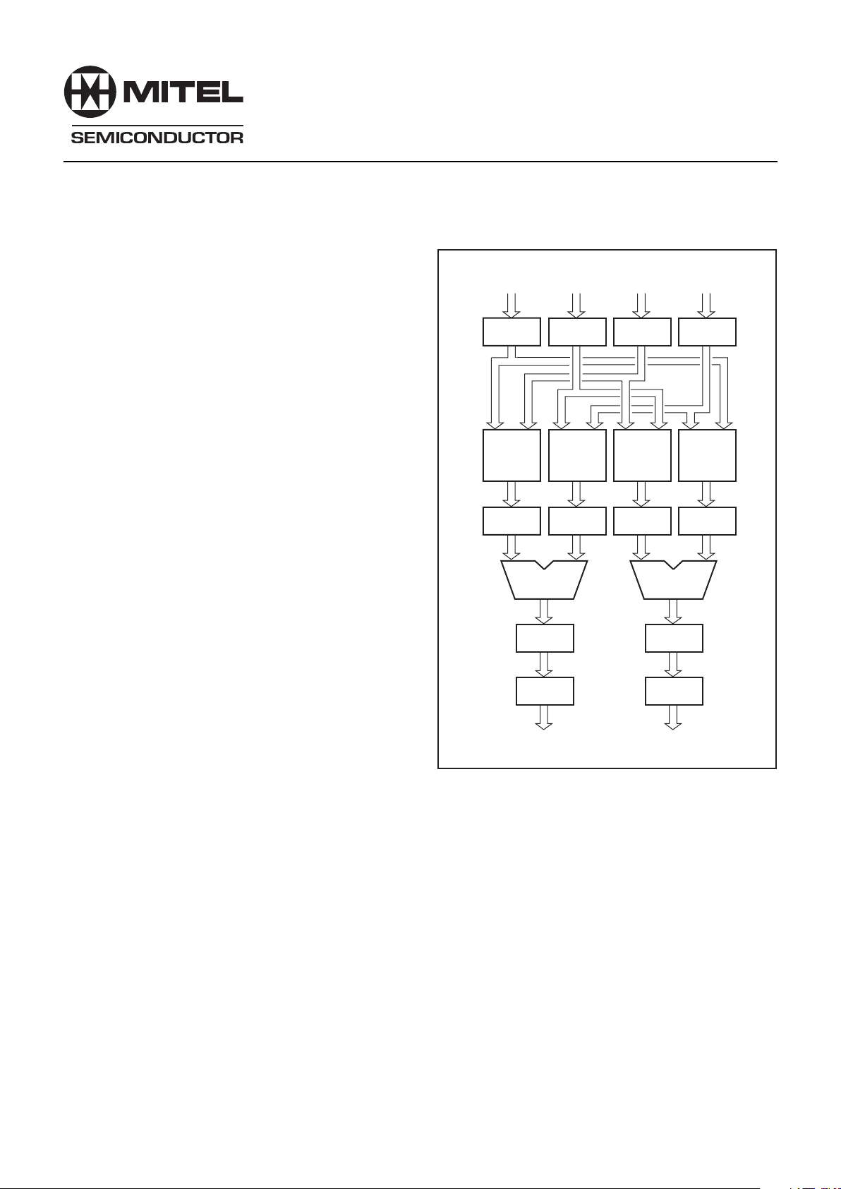
Fig. 1 Simplified block diagram
PR15:0
ADD/SUB
REG
MULT
REG
REG
MULT
REG
REG
MULT
REG
REG
MULT
REG
ADD/SUB
SHIFT
REG
SHIFT
REG
PI15:0
XR15:0 XI15:0 YR15:0 YI15:0
The PDSP16116 contains four 16316 array multipliers, two
32-bit adder/subtractors and all the control logic required to support Block Floating Point Arithmetic as used in FFT applications.
The PDSP16116A variant will multiply two complex (16116)
bit words every 50ns and can be configured to output the complete complex (32132) bit result within a single cycle. The data
format is fractional two’s complement.
In combination with a PDSP16318A, the PDSP16116A forms
a two-chip 20MHz complex multiplier accumulator with 20-bit
accumulator registers and output shifters. The PDSP16116A in
combination with two PDSP16318As and two PDSP1601As
forms a complete 20MHz Radix 2 DIT FFT butterfly solution
which fully supports block floating point arithmetic. The
PDSP16116 has an extremely high throughput that is suited to
recursive algorithms as all calculations are performed with a
single pipeline delay (two cycle fall-through).
Page 2

PDSP16116
2
SYSTEM FEATURES
The PDSP16116 has a number of features tailored for system applications.
(21)3(21) Trap
In multiply operations using two’s complement fractional notation, the (21)3(21) operation forms an invalid result because
11 is not representable in the fractional number range. The
PDSP16116 eliminates this problem by trapping the (21)3(21)
operation and forcing the multiplier result to become the most
positive representable number.
Complex Conjugation
Many algorithms using complex arithmetic require conjugation of complex data stream. This operation has traditionally required an additional ALU to multiply the imaginary component
by -1. The PDSP16116 eliminates this requirement by offering
on-chip complex conjugation of either of the two incoming complex data words with no loss in throughput.
Easy Interfacing
As with all PDSP family members the PDSP16116 has registered l/O for data and control. Data inputs have independent
clock enables and data outputs have independent three state
output enables.
Signal
XR15:0
Xl15:0
YR15:0
Yl15:0
PR15:0
Pl15:0
CLK
CONX
CONY
ROUND
MBFP
AR15:1 3
Al15:1 3
WTA1:0
WTB1:0
WTOUT1:0
SFTA1:0
SFTR2:0
GWR4:0
OSEL1:0
V
DD
GND
Type
Input
Input
Input
Input
Output
Output
Input
Input
Input
Input
Input
Input
Input
Input
Input
Input
Input
Input
Input
Output
Output
Output
Output
Input
Input
Power
Power
Description
16-bit input for real X data
16-bit input for imaginary X data
16-bit input for real Y data
16-bit input for imaginary Y data
16-bit output for real P data
16-bit output for imaginary P data
Clock; new data is loaded on rising edge of CLK
Clock, enable X-port input register
Clock, enable Y-port input register
Conjugate X data
Conjugate Y data
Rounds the real and imaginary results
Mode select (BFP/Normal)
Start of BFP operations (see Note 1)
End of pass (See Note 1)
3 MSBs from real part of A-word (See Note 1)
3 MSBs from imaginary part of A-word (See Note 1)
Word tag from A-word
Word tag from B-word/shift control (See Note 2)
Word tag output (See Note 1)
Shift control for A-word / overflow flag (See Note 2)
Shift control for accumulator result (See Note 1)
Global weighting register contents (See Note 1)
Selects the desired output configuration
Output enables
15V Supply (See Note 3)
0V Supply (See Note 3)
Normal
mode
configuration
Tie low
Tie low
Tie low
Tie low
Tie low
Tie low
NOTES
1. Used only in BFP mode
2. Performs different functions in BFP/Normal modes
3. All supply pins must be connected
Table 1 Signal descriptions
CEX
CEY
SOBFP
EOPSS
OER, OEI
Page 3
PDSP16116
3
Fig. 2 PDSP16116 Block diagram
ADD/SUB
DECODE
REG
REG
16316
MULT
MUX
XR15:0
C
O
M
P
REG
REG
MUX
XI15:0
C
O
M
P
REG
REG
MUX
YR15:0
C
O
M
P
REG
REG
MUX
YI15:0
C
O
M
P
16316
MULT
16316
MULT
16316
MULT
ADD/SUB
CONX CONY
SHIFT
REG
SHIFT
REG
MUX MUX
OVR
CEYCEX
CONTROL
LOGIC
CLK
WTA
AR15:13
WTB
AI15:13
SOBPF
EOPSS
SFTR
SFTA
GWR4:0
WTOUT
ROUND
OSEL
ROUND
OSEL
OER OEI
PR15:0 PI15:0
INTERNAL
SIGNALS
‘1’
Page 4
PDSP16116
4
1
2
3
4
5
6
7
8
9
10
11
12
13
14
15
A B C D E F G H J K L M N P R
PIN 1 IDENT
(SEE NOTE 2)
PIN 144
PIN 1
Fig. 3a Pin connections for 144 I/O power pin grid array package (bottom view)
Fig. 3b Pin connections for 144 I/O ceramic quad flatpack (top view)
Fig. 3 Pin connection diagrams (not to scale). See Table 1 for signal descriptions and Table 2 for pinouts.
AC144 (POWER)
GG144
Page 5

PDSP16116
5
Signal
V
DD
GND
PR13
PR12
PR11
PR10
PR9
PR8
PR7
PR6
PR5
GND
V
DD
PR4
PR3
PR2
PR1
PR0
PI0
PI1
PI2
PI3
PI4
V
DD
PI5
GND
PI6
PI7
PI8
PI9
PI10
PI11
PI12
PI13
GND
V
DD
GG
1
2
3
4
5
6
7
8
9
10
11
12
13
14
15
16
17
18
19
20
21
22
23
24
25
26
27
28
29
30
31
32
33
34
35
36
Signal
PI14
PI15
WTOUT1
WTOUT0
SFTR0
SFTR1
SFTR2
OEI
CONY
CONX
ROUND
AI13
AI14
AI15
AR13
AR14
AR15
YI15
YI14
YI13
YI12
YI11
YI10
YI9
YI8
YI7
YI6
YI5
YI4
YI3
YI2
YI1
YI0
XI0
GND
V
DD
AC
D3
C2
B1
D2
E3
C1
E2
D1
F2
F3
E1
G2
G3
F1
G1
H2
H1
H3
J3
J1
K1
J2
K2
K3
L1
L2
M1
N1
M2
L3
N2
P1
M3
N3
B2
A1
GG
37
38
39
40
41
42
43
44
45
46
47
48
49
50
51
52
53
54
55
56
57
58
59
60
61
62
63
64
65
66
67
68
69
70
71
72
Signal
XI1
XI2
XI3
XI4
XI5
XI6
XI7
XI8
XI9
XI10
XI11
XI12
XI13
XI14
XI15
CEY
CEX
XR15
XR14
XR13
XR12
XR11
XR10
XR9
XR8
XR7
XR6
XR5
XR4
XR3
XR2
XR1
XR0
YR15
YR14
YR13
AC
N4
P3
R2
P4
N5
R3
P5
R4
N6
P6
R5
P7
N7
R6
R7
P8
R8
N8
N9
R9
R10
P9
P10
N10
R11
P11
R12
R13
P12
N11
P13
R14
N12
N13
P14
R15
GG
73
74
75
76
77
78
79
80
81
82
83
84
85
86
87
88
89
90
91
92
93
94
95
96
97
98
99
100
101
102
103
104
105
106
107
108
Signal
GND
V
DD
YR12
YR11
YR10
YR9
YR8
YR7
YR6
YR5
YR4
YR3
YR2
YR1
YR0
EOPSS
V
DD
SOBFP
WTB1
WTB0
WTA1
WTA0
MBFP
CLK
OSEL1
OSEL0
OER
SFTA0
SFTA1
GWR0
GWR1
GWR2
GWR3
GWR4
PR15
PR14
AC
P2
R1
P15
M14
L13
N15
L14
M15
K13
K14
L15
J14
J13
K15
J15
H14
H15
H13
G13
G15
F15
G14
F14
F13
E15
E14
D15
C15
D14
E13
C14
B15
D13
C13
B14
A15
GG
109
110
111
112
113
114
115
116
117
118
119
120
121
122
123
124
125
126
127
128
129
130
131
132
133
134
135
136
137
138
139
140
141
142
143
144
AC
N14
M13
A14
B12
C11
A13
B11
A12
C10
B10
A11
B13
C12
A10
A9
B8
A8
C8
C7
A7
A6
B7
B6
C6
A5
B5
A4
A3
B4
C5
B3
A2
C4
C3
B9
C9
NOTE. All GND and VDD pins must be used
Table 2 Pin connections for AC144 (Power) and GG144 packages
Page 6
PDSP16116
6
NORMAL MODE OPERATION
When the MBFP mode select input is held low the ‘Normal’
mode of operation is selected. This mode supports all complex
multiply operations that do not require block floating point
arithmetic.
Complex two’s complement fractional data is loaded into the
X and Y input registers via the X and Y Ports on the rising edge
of CLK. The X and Y port registers are individually enabled by
the
CEX
and
CEY
signals respectively. If the registers are required to be permanently enabled, then these signals may be
tied to ground.
The Real and Imaginary components of the fractional data
are each assumed to have the following format:
Bit Number
15
Weighting
14131211109 76543210
S
2
–
15
2
–
14
2
–
13
2
–
12
2
–
11
2
–
10
2
–
9
2
–
8
2
–
6
2
–
5
2
–
4
2
–
3
2
–
2
2
–
1
8
2
–
7
Where S = sign bit, which has an effective weighting of 22
0
The value of the 16-bit two’s complement word is (213S)1(bit143221)1(bit133222)1(bit123223) …
Multiplier Stage
On each clock cycle the contents of the input registers are passed
to the four multipliers to start a new complex multiply operation.
Each complex multiply operation requires four partial products
(XR3YR), (XR3YI), (XI3YR), (XI3YI), all of which are calculated
in parallel by the four 16316 multipliers. Only one clock cycle is
required to complete the multiply stage before the multiplier results
are loaded into the multiplier output registers for passing on to the
adder/ subtractors in the next cycle. Each multiplier produces a 31bit result with the duplicate sign bit eliminated. The format of the
output data from the multipliers is:
Bit Number
30
Weighting
292827262524 76543210
≈ ≈ ≈
S
2
–
30
2
–
29
2
–
28
2
–
27
2
–
26
2
–
25
2
–
24
2
–
23
2
–
6
2
–
5
2
–
4
2
–
3
2
–
2
2
–
1
The effective weighting of the sign bit is 22
0
Adder/Subtractor Stage
The 31-bit real and imaginary results from the multipliers
are passed to two 32-bit adder/subtractors. The adder calculates the imaginary result [(XR 3 YI) 1 (XI 3 YR)] and the
Rounding
The ROUND control when asserted rounds the most
significant 16 bits of the full 32-bit result from the shifter. If the
ROUND signal is active (high), then bit 16 is set to ‘1’, rounding
the most significant 16 bits of the shifted result. (The least
significant 16 bits are unaffected). Inserting a ‘1’ ensures that
the rounding error is never greater than 1 LSB and that no DC
bias is introduced as a result of the rounding processes. The
format of the rounded result is:
The effective weighting of the sign bit is 22
1
Bit Number
30
Weighting
29 28 27 17 16 15 14 13 2 1 0
≈ ≈ ≈
S
2
–
30
2
–
29
2
–
28
2
–
17
2
–
16
2
–
15
2
–
14
2
–
13
2
–
3
2
–
2
2
–
1
2
0
31 18
2
–
1
2
≈ ≈ ≈
ROUNDED VALUE
LSBs
The effective weighting of the sign bit is 22
1
Bit Number
30
Weighting
29282726 76543210
≈ ≈ ≈
S
2
–
30
2
–
29
2
–
28
2
–
27
2
–
26
2
–
25
2
–
24
2
–
23
2
–
4
2
–
3
2
–
2
2
–
1
2
0
31 8
2
–
22
subtractor calculates the real result (XR 3 YR) = (XI 3 YI).
Each adder/subtractor produces a 32-bit result with the
following format:
Result Correction
Due to the nature of the fraction two’s complement representation it is possible to represent 21 exactly but not 11. With
conventional multipliers this causes a problem when 21 is multiplied by 21 as the multiplier produces an incorrect result. The
PDSP16116 includes a trap to ensure that the most positive
number (value = 1·2
230
, hex = 7FFFFFFFF) is substituted for
the incorrect result. The multiplier result is therefore always a
correct fractional value. Fig.2 shows the value ‘1’ being multiplexed into the data path controlled by four comparators.
Complex Conjugation
Either the X or Y input data may be complex conjugated by
asserting the CONX or CONY signals respectively. Asserting
either of these signals has the effect of inverting (multiplying
by 21 ) the imaginary component of the respective input. Table 3
shows the effect of CONX and CONY on the X and Y inputs.
Table 3 Conjugate functions
CONYCONX
Low
High
Low
High
Low
Low
High
High
Function
(XR 1 XI)3(YR 1 YI)
(XR 2 XI)3(YR 1 YI)
(XR 1 XI)3(YR 2 YI)
Invalid
Operation
X 3 Y
Conj. X 3 Y
X 3 Conj. Y
Invalid
Page 7

PDSP16116
7
Shifter
Each of the two adder/subtractors are followed by shifters
controlled via the WTB control input. These shifters can each
apply two different shifts; however, the same shift is applied to
both real and imaginary components. The four shift options are:
1. WTB1:0 = 11 Shift complex product one place to the left, giving a shifter output format:
Bit Number
30
Weighting
29282726 76543210
≈ ≈ ≈
S
2
–
30
2
–
29
2
–
28
2
–
27
2
–
26
2
–
25
2
–
24
2
–
4
2
–
3
2
–
2
2
–
1
31 25
2
–
5
2
–
6
2
–
31
The effective weighting of the sign bit is 22
0
Bit Number
30
Weighting
29282726 76543210
≈ ≈ ≈
S
2
–
30
2
–
29
2
–
28
2
–
27
2
–
26
2
–
25
2
–
24
2
–
4
2
–
3
2
–
2
2
0
31
2
–
1
8
2
–
22
2
–
23
2. WTB1:0 = 00 No shift applied, giving a shifter output format:
Bit Number
30
Weighting
29282726 6543210
≈ ≈ ≈
S
2
–
29
2
–
28
2
–
27
2
–
26
2
–
25
2
–
24
2
–
4
2
–
3
2
–
2
2
0
31
2
–
1
2
–
23
2
1
25
2
–
5
24
The effective weighting of the sign bit is 22
2
The effective weighting of the sign bit is 22
1
The effective weighting of the sign bit is 22
3
4. WTB1:0 = 10 Shift complex product two places to the right, giving a shifter output format:
Bit Number
30
Weighting
29282726 6543210
≈ ≈ ≈
S
2
–
28
2
–
27
2
–
26
2
–
25
2
–
24
2
–
4
2
–
3
2
–
2
2
0
31
2
–
1
2
–
23
2
1
25 24
2
2
2
–
22
3. WTB1:0 = 01 Shift complex product one place to the right, giving a shifter output format:
PIN DESCRIPTIONS
XR, XI, YR, YI
Data inputs, 16 bits. Data is loaded into the input registers
from these ports on the rising edge of CLK. The data format is
fractional two’s complement, where the MSB (sign bit) is bit 15.
In normal mode the weighting of the MSB is 22
0
i.e. 21.
PR, PI
Data outputs, 16 bits. Data is clocked into the output registers and passed to the PR and PI outputs on the rising edge of
CLK. The data format is fractional two’s complement. The field
of the internal result selected for output via PR and PI is controlled by signals OSEL1:0 (see Table 4).
CLK
Common clock to all internal registers
Clock enables for X and Y input ports. When low these inputs
enable the CLK signal to the X or Y input registers, allowing
new data to be clocked into the Multiplier.
CONX, CONY
Conjugate controls. If either of these inputs is high on the
rising edge of CLK, then the data on the associated input has its
imaginary component inverted (multiplied by 21), see Table 3.
CONX and CONY affect data input on the same clock rising
edge.
ROUND
The ROUND control pin is used to round the most significant 16
bits of the output register. The ROUND input is not latched and is
intended to be tied high or low depending upon the application.
MSR and LSR are the most and least siginificant 16-bit words
of the real shifter output, MSl and LSl are the most and least
significant 16-bit words of the imaginary shifter output.
The output select options allow two different modes for extracting the full 32-bit result from the PDSP16116. The first mode
treats the two 16-bit outputs as real and imaginary ports, allowing the real and imaginary results to be output in two halves on
the real and imaginary output ports. The second mode treats
the two 16-bit outputs as one 32-bit output and allows the real
and imaginary results to be output as 32-bit words.
Table 4 Output selection
Overflow
If the left shift option is selected and the adder/subtractor
contains a 32-bit word, then an invalid result will be passed to
the output. An invalid output arising from this combination of
events will be flagged by the SFTA0 flag output. The SFTA0 flag
will go high if either the real or imaginary result is invalid.
Output Select
The output from the shifters is passed to the output select
mux, which is controlled via the OSEL inputs. These inputs are
not registered and hence allow the output combination to be
changed within each cycle. The full complex 64-bit result from
the multiplier may therefore be output within a single cycle. The
OSEL control selects four different output combinations as
summarised in Table 4.
OSEL1
0
1
0
1
P1PROSEL0
MSR
LSR
MSR
MSI
0
0
1
1
MSI
LSI
LSR
LSI
CEX, CEY
Page 8

PDSP16116
8
MBFP
Mode select. When high, block floating point (BFP) mode is
selected. This allows the device to maintain the dynamic range
of the data using a series of word tags. This is especially useful
in FFT applications. When low, the chip operates in normal mode
for more general applications. This pin is intended to be tied
high or low, depending on application.
WTOUT1:0 (BFP Mode Only)
Word tag output. This tag records the weighting of the output
words from the current cycle relative to the current global
weighting register (see Table 6). It should be stored along with
the A
′ and B′ words as it will form the input word tags, WTA and
WTB, for each complex word during the next pass. In normal
mode, WTOUT1:0 are not used and should be left unconnected.
Weighting of the output relative to
the current global weighting register
WTOUT1:0
One less
The same
One more
Two more
00
01
10
11
Table 6 Word tag weightings
Function
WTB1:0
Shift complex product 1 place to the left
No shift applied
Shift complex product 1 place to the right
Shift complex product 2 places to the right
11
00
01
10
Table 7 Normal mode shift control
SFTA1:0 (BFP and Normal Modes)
In BFP mode, these signals act as the A-word shift control.
They allow shifting from one to four places to the right, (see
Table 8). Depending on the relative weightings of the A-words
and the complex product, the A-word may have to be shifted to
the right to ensure compatible weightings at the inputs to the
PDSP16318 complex accumulator. The two words must have
the same weighting if they are to be added.
In normal mode, SFTA0 performs a different function. If
WTB1:0 is set to implement a left shift, then overflow will occur
if the data is fully 32 bits wide. This pin is used to flag such an
overflow. SFTA1 is not used in normal mode.
Function
SFTA1:0
Shift A-word 1 place to the right
Shift A-word 2 places to the right
Shift A-word 3 places to the right
Shift A-word 4 places to the right
00
01
10
11
WTA1:0 (BFP Mode Only)
Word tag from the A-word. This word records the weighting
of the A-word relative to the global weighting register on the
previous pass. Although the A-word itself is not processed in the
PDSPl 6116, this information is required by the control logic for
the radix 2 butterfly FFT application. These inputs should be
tied low in normal mode.
WTB1:0 (BFP and Normal Modes)
In BFP mode, this is the word tag from the B-word. This is
operated in the same manner as WTA but for the B-word. The
value of the word tags are used to ensure that the binary weighting of the A-word and the product of the complex multiplier are
the same at the inputs to the complex accumulator. Depending
on which word is the larger, the weighting adjustment is performed using either the internal shifter or an external shifter controlled by SFTA. The word tags are also used to maintain the
weighting of the final result to within plus two and minus one
binary points relative to the new GWR. (On the first pass all
word tags will be ignored). In normal mode. these inputs perform a different function. They directly control the internal shifter
at the output port as shown in Table 7.
Table 8 External A-word shift control
GWR4:0 (BFP Mode Only)
Contents of the global weighting register. The GWR stores
the weighting of the largest word present with respect to the
weighting of the original input words. Hence, if the contents of
the GWR are 00010, it indicates that the largest word currently
being processed has its binary point two bits to the right of the
original data at the start of the BFP calculations.
The contents of this register are updated at the end of each
pass, according to the largest value of WTOUT occuring during
that pass. For example, if WTOUT = 11, then GWR will be
increased by 2 (see Table 6). The GWR is presented in two’s
complement format. In normal mode, GWR4:0 are not used and
should be left unconnected.
Start of BFP. This input should be held low for the first cycle
of the first pass of the BFP calculations (see Fig.7). It serves to
reset the internal registers associated with BFP control. When
operating in normal mode this input should be tied low.
End of pass. This input should be held low for the last cycle
of each pass and for the lay time between passes. It instructs
the control logic to update the value of the global weighting register and prepare the BFP circuitry for the next pass. When operating in normal mode this input should be tied low.
AR15:13 (BFP Mode Only)
Three MSBs of the real part of the A-word. These are used
in the FFT butterfly application (see Fig. 4) to determine the
magnitude of the real part of the A-word and, hence, to determine if there will be any change of word growth in the
PDSP16318 Complex Accumulator. When operating in normal
mode, these inputs are not used and may be tied low.
AI15:13 (BFP Mode Only)
Three MSBs of the imaginary part of the A-word. Used in the
same fashion as AR15:13.
SFTR2:0 (BFP Mode Only) Accumulator result shift control.
These pins should be linked directly to the S2:0 pins on the
PDSP16318 Complex Accumulator. They control the
accumulator’s barrel shifter (see Table 5). The purpose of this
shift is to minimise sign extension in the multiplier or accumulator
ALUs. In normal mode, SFTR2:0 are not used and should be
left unconnected.
Table 5 Accumulator shifts (BFP mode)
SFTR2:0
000
001
010
011
100
101
110
111
Reserved
Reserved
Reserved
Shift right by one
No shift
Shift left by one
Shift left by two
Reserved
Function
SOBFP (BFP Mode Only)
EOPSS (BFP Mode Only)
Page 9

PDSP16116
9
OSEL1 :0
The outputs from the device are selected by the OSEL0
and OSEL1 instruction bits. These controls allow selection
of the output combination during the current cycle (they are
not registered). There are four possible output configurations
that allow either complex outputs of the most or least significant bytes, or real or imaginary outputs of the full 32-bit word
(see Table 4). OSEL0 and OSEL1 should both be tied low
when in BFP mode.
BFP MODE FFT APPLICATION
The PDSP16116 may be used as the main arithmetic unit of
the butterfly processor, which will allow the following FFT benchmarks:
● 1024-point complex radix 2 transform in 517µs
● 512-point complex radix 2 transform in 235µs
● 256-point complex radix 2 transform in 106µs
In addition, with pin MBFP tied high, the BFP circuitry within
the PDSP16116 can be used to adaptively rescale data throughout the course of the FFT so as to give high-resolution results.
The BFP system on the PDSP16116 can be used with any variation of the radix 2 decimation-in-time (DIT) FFT, for example,
the constant geometry algorithm, the in-place algorithm etc. An
N-point Radix 2 DIT FFT is split into log(N) passes. Each pass
consists of N/2 ‘butterflies’, each performing the operation:
A
′ = A1BW
B
′ = A2BW
Where W is the complex coefficient and A and B are the
complex data. Fig.4 illustrates how a single PDSP16116 may
be combined with two PDSP1601s and two PDSP16318s to
form a complete BFP butterfly processor. The PDSP16318s are
used to perform the complex addition and subtraction of the
butterfly operation, while the PDSP1601s are used to match
the data path of the A-word to the pipelining and shifting operations within the PDSP16116.
For more information on the theory and construction of this
butterfly processor, refer to application note AN59.
BFP MODE OPERATION
The BFP mode on the PDSP16116 is intended for use in the
FFT application described above, that is, it is intended to prevent data degradation during the course of an FFT calculation.
The operation of the PDSP16116-based BFP buttertly processor (see Fig.4) is described below.
The Block Floating Point System
A block floating point system is essentially an ordinary integer arithmetic system with some additional logic, the purpose of
which is to lend the system some of the enormous dynamic
range afforded by a true floating point system without suffering
the corresponding loss in perlormance.
The initial data used by the FFT should all have the same
binary arithmetic weighting. In other words, the binary point
should occupy the same position in every data word as is normal in integer arithmetic. However, during the course of the FFT,
a variety of weightings are used in the data words to increase
the dynamic range available. This situation is similar to that within
a true floating point system, though the range of numbers representable is more limited. In the BFP system used in the
PDSP16116, there are, within any one pass of the FFT, four
possible positions of the binary point wihin the integer words. To
record the position of its binary point, each word has a 2-bit
word tag associated with it. By way of example, in a particular
pass the following four positions of binary point may be available, each denoted by a certain value of word:
XX·XXXXXXXXXXXX word tag = 00
XXX·XXXXXXXXXXX word tag = 01
XXXX·XXXXXXXXXX word tag = 10
XXXXX·XXXXXXXXX word tag = 11
At the end of each constituent pass of the FFT, the positions
of the binary point supported may change to reflect the trend of
data increase or decreases in magnitude. Hence, in the pass
following that of the above example, the four positions of binary
point supported may be changed to:
XX·XXXXXXXXXXXX word tag = 00
XXX·XXXXXXXXXXX word tag = 01
XXXX·XXXXXXXXXX word tag = 10
XXXXX·XXXXXXXXX word tag = 11
This variation in the range of binary points supported from
pass to pass (i.e. the movement of the binary point relative to its
position in the original data) is recorded in the GWR. Thus, the
position of the binary point can be determined relative to its initial position by modifying the value of GWR by WTOUT for a
given word as shown in Table 6. As an example, if GWR=01001
and WTOUT=10 then the binary point has moved 10 places to
the right of its original position.
PDSP16116/A
XR XI YR YI
BR BI WR WI
WTA WTB
EOPSSSOBFP
PR PI
PDSP1601/A
A
C
AI
AI15:13
PDSP1601/A
A
C
AR
AR15:13
PDSP16318/A
AB
CD
PDSP16318/A
BA
CD
WTOUT GWRA′RA′IB′RB′I
DAR DAI
SFTASFTA
SFTR SFTR
OER OEI
Fig. 4 FFT butterfly processor
Page 10

PDSP16116
10
The butterfly operation
The butterfly operation is the arithmetic operation which is
repeated many times to produce an FFT. The PDSP16116- based
butterfly processor performs this operation in a low power high
accuracy chip set.
A new butterfly operation is commenced each cycle, requiring a new set ot data for B, W, WTA and WTB. Five cycles later,
the corresponding results A′ and B′ are produced along with
their associated WTOUT. In between, the signals SFTA and
SFTR are produced and acted upon by the shifters in the
PDSP1601/A and PDSP16318/A. The timing of the data and
control signals is shown in Fig.6.
The results (A′ and B′) of each butterfly calculation in a pass
must be stored to be used later as the input data (A and B) in
the next pass. Each result must be stored together with its associated word tag, WTOUT. Although WTOUT is common to
both A′ and B′, it must be stored separately with each word as
the words are used on different cycles during the next pass. At
the inputs, the word tag associated with the A word is known as
WTA and the word tag associated with the B word is known as
WTB. Hence, the WTOUTs from one pass will become the WTAs
and WTBs for the following pass. It should be noted that the first
pass is unique in that word tags need not be input into the butterfly as all data initially has the same weighting. Hence, during
the first pass alone, the inputs WTA and WTB are ignored.
Fig. 5 Butterfly operation
Control of the FFT
To enable the block floating point hardware to keep track of
the data, the following signals are provided:
SOBFP
- start of the FFT
EOPSS
- end of current pass
These inform the PDSPl 6116/A when an FFT is starting and
when each pass is complete. Fig.7 shows how these signals
should be used and a commentary is provided below.
To begin the FFT, the signal
EOPSS
should be set high
(where it will remain for the duration of the pass).
SOBFP
should
be pulled low during the initial cycle when the first data words
A and B are presented to the inputs of the butterfly processor.
The following cycle
SOBFP
must be pulled high where it should
remain for the duration of the FFT. New data is presented to the
processor each successive cycle until the end of the first pass
of the FFT. On the last cycle of the pass, the
EOPSS
should be
pulled low and held low for a minimum of five cycles, the time
required to clear the pipeline of the butterfly processor so that
all the results from one pass are obtained before beginning the
following pass.
Should a longer pause be required between passes – to ar-
range the data for the next pass, for example – then
EOPSS
may
CLK
n11
n
1
2
n13
n
1
4
n
1
4
n11
n
1
2
n13
n
1
4
n
1
4
n11
n
1
2
n13
n
1
4
n
1
4
n21
n
1
1
n
1
2
n
1
3
n22
n
1
1
n
1
2
n11
n
1
2
n11
n
1
2
n24
n
2
3
n22
n
2
1
n11
n
2
1
n
n
n
n
n
n
n
n
n
n
2
2
n23
n23
n23
n25
n25
n22
n22
n21
n21
n21
n23n
2
2
BR, BI, WR, WI
WTA, WTB
AR, AI
SFTA
SFTR
PR, PI
DAR, DAI
WTOUT
A′R, A′I, B′R, B′I
Fig. 6 Butterfly data and control signals
FFT Output Normalisation
When an FFT system outputs a series of FFT results for
display, storage or transmission, it is essential that all results
are compatible, i.e. with the binary point in the same position.
However, in order to preserve the dynamic range of the data in
the FFT calculation, the PDSP1601/A employs a range of different weightings. Therefore, data must be re-formatted at the
end of the FFT to the pre-determined common weighting. This
can be done by comparing the exponent of given data word
with the pre-determined universal exponent and then shifting
the data word by the difference. The PDSP1601/A, with its
multifunction 16-bit barrel shifter, is ideally suited to this task.
According to theory, the largest possible data result from an
FFT is N times the largest input data. This means that the binary point can move a maximum of log
2
(N) places to the right.
Hence, if the universal exponent is chosen to be log2(N) this
should give a sufficient range to represent all data points faithfully.
AA′
BB′
A′ = A1BW
B′ = A2BW
W
be kept low as long as necessary; the next pass cannot commence until it is brought high again. On the initial cycle of each
new pass, the signal
EOPSS
should be pulled high and it should
remain high until the final cycle of that pass, when it is pulled
low again.
Page 11

PDSP16116
11
CLK
n
2
4n23n22n21
n
2
5
A′, B′, BTOUT
SOBFP
EOPSS
A, B, W,
WTA, WTB
GWR
234567
n
2
123
23
11 n 1
1 n
START OF
FIRST PASS
END OF FIRST PASS/
START OF NEXT PASS
(MINIMUM NUMBER OF
LAY CYCLES SHOWN).
PERIOD BETWEEN
OTHER INTERMEDIATE
PASSES IS SIMILAR.
NOTES
1. 1 = FIRST CYCLE OF DATA IN PASS
2. n = LAST CYCLE OF DATA IN PASS
In practice, data output may never approach the theoretical
maximum. Hence, it may be worthwhile to try various universal
exponents and choose the one best suited to the particular application.
Data is output from the butterfly processor with a two-part
exponent: the 5-bit GWR applicable to all data words from a
given FFT and a 2-bit WTOUT associated with each individual
dataword. To find the complete exponent for a given word, the
GWR for that FFT must be modified by its WTOUT as shown in
Table 6. The result is the number of places the binary point has
shifted to the right during the course of the FFT.
This value must be compared with the universal exponent to
determine the shift required. This is done by subtracting it from
the universal exponent. The number of places to be shifted is
equal to the difference between the two exponents. The shift
can be implemented in a PDSP1601/A (the shift value is fed
into the SV port).
As FFT data consists of real and imaginary parts, either two
PDSP1601/As must be used (controlled by the same logic) or a
single PDSP1601/A could be used handling real and imaginary
data on alternate cycles (using the same instructions for both
cycles).
An example of an output normalisation circuit is shown
in Fig.8. Only 4-bit data paths are used in calculating the
shift. This means that we must be able to trap very small
values negative of GWR and force a 15-bit right shift in
such cases.
NB It is easier to simply add the word tag to the exponent for the
purpose of determing the shift required, instead of modifying it
according to Table.6. To compensate for this, the universal exponent may be increased by one.
Fig. 8 Output normalisation circuit
4-BIT ADDER
GWRWTOUT
4-BIT SUBTRACTOR
UNIVERSAL
EXPONENT
4-BIT MUX
1111
SIGN
BIT
16-BIT DATA
PDSP1601
SV PORT B PORT
C PORT
ASRSV
NORMALISED OUTPUT DATA
Fig. 7 Use of the BFP control signals
Page 12

PDSP16116
12
CLK
INPUT DATA X AND Y
OUTPUT P PORTS
OUTPUT SFTA1:0
VALID DATA
INPUT CONTROLS CEX AND CEY
t
CP
t
DS
t
DH
t
CLK
t
CLKH
t
CLKL
t
CSFTA
t
CSFTA
VALID DATA
t
CONS
t
CES
t
CEH
t
CONH
t
WS
t
WH
INPUT CONTROLS CONX AND CONY
INPUT CONTROL WTB1:0
Fig. 9 Normal mode timing
OER AND OEI
OUTPUT P PORTS
HIGH Z
t
OPLZ
t
OPZL
HIGH Z
t
OPZH
t
OPHZ
HIGH Z
Fig. 10 Output tristate timing
V
H
0·5V
Delay from
output high
to output
high Z (t
OPHZ
)
0·5V
0·5V
0·5V
V
L
1·5V
1·5V
Delay from
output low
to output
high Z (t
OPLZ
)
Delay from
output high Z
to output low
(t
OPZL
)
Delay from
output high Z
to output high
(t
OPZH
)
Test Waveform measurement level
V
H
is the voltage reached when the output is driven high
VL is the voltage reached when the output is driven low
VT = 0V
VT = V
DD
Three state delay measurement load
V
T
DUT
30p
1·5k
Fig. 11 Three state delay measurement
Page 13

PDSP16116
13
ELECTRICAL CHARACTERISTICS
The Electrical Characteristics are guaranteed over the following range of operating conditions, unless otherwise stated:
VDD = 15V±10%, GND = 0V, T
AMB
(Industrial) = 240°C to 185°C, T
AMB
(Military) = 255°C to 1125°C
Static Characteristics
Min. Typ. Max.
Output high voltage
Output low voltage
Input high voltage
Input high voltage
Input low voltage
Input leakage current
Input capacitance
Output leakage current
Output short circuit current
10
-
0·4
-
-
0·8
110
150
300
2·4
3·0
2·2
-
210
250
10
V
OH
V
OL
V
IH
V
IH
V
IL
I
IN
C
IN
I
OZ
I
OS
IOH = 8mA
I
OL
= 28mA
CLK input only
All other inputs
GND < V
IN
< V
DD
GND < V
OUT
< V
DD
VDD = 15·5V
V
V
V
V
V
µA
pF
µA
mA
Units
Value
Conditions
Characteristic Symbol
P ports setup time
WTOUT1:0 setup time
GWR4:0 setup time
SFTA1:0 setup time
SFTR2:0 setup time
CEXorCEY
setup time
CEXorCEY
hold time
X or Y ports setup time
X or Y ports hold time
WTA, WTB,
SOBFP or EOPSS
setup time
WTA, WTB,
SOBFP or EOPSS
hold time
CONX or CONY setup time
CONX or CONY hold time
AR15:13 or AI15:13 setup time
AR15:13 or AI15:13 hold time
OSEL to valid P ports
OER or OEI
high to PR or PI high to high Z
OER or OEI
low to PR or PI low to high Z
OER or OEI
low to PR or PI high Z to high
OER or OEI
high to PR or PI high Z to low
CLK frequency
CLK period
CLK high time
CLK low time
V
DD
current (CMOS input levels)
V
DD
current (TTL input levels)
Characteristic
Switching Characteristics
Symbol
t
CP
t
CW
t
CG
t
CSFTA
t
CSFTR
t
CES
t
CEH
t
DS
t
DH
t
WS
t
WH
t
CONS
t
CONH
t
AS
t
AH
t
OP
t
OPHZ
t
OPLZ
t
OPZH
t
OPZL
f
CLK
t
CLK
t
CLKH
t
CLKL
I
DDC
I
DDT
Max.
Min. Max. Min.
45
30
30
60
50
-
0
-
2
-
0
-
0
-
0
35
35
45
22
24
10
-
-
-
60
100
5
5
5
5
5
11
-
11
-
14
-
14
-
14
-
-
-
-
-
-
100
30
20
-
-
PDSP16116A
5
5
5
5
5
8
-
8
-
8
-
8
-
8
-
-
-
-
-
-
50
12
12
-
-
23
20
20
30
28
-
0
-
0
-
0
-
0
-
0
20
25
25
18
18
20
-
-
-
80
130
PDSP16116
Conditions
NOTES
1. VDD = 15·5V, outputs unloaded, clock frequency = Max.
2. The PDSP16116B is specified as the PDSP16116A except that the maximum clock frequency is guaranteed at 25MHz, with a minimum
clock period of 40ns.
Fig.
9
9
9
9
9
9
9
9
9
9
10, 11
10, 11
10, 11
10, 11
9
9
9
Max.
Min.
PDSP16116D
5
5
5
5
5
8
-
8
-
8
-
8
-
8
-
-
-
-
-
-
31·7
12
12
-
-
23
20
20
30
28
-
0
-
2
-
0
-
0
-
2
20
25
25
18
18
31·5
-
-
-
80
130
Units
30pF
30pF
30pF
30pF
30pF
30pF
See Note 1
See Note 1
ns
ns
ns
ns
ns
ns
ns
ns
ns
ns
ns
ns
ns
ns
ns
ns
ns
ns
ns
ns
MHz
ns
ns
ns
mA
Page 14

PDSP16116
14
ABSOLUTE MAXIMUM RATINGS (NOTE 1)
Supply voltage, V
DD
Input voltage, V
IN
Output voltage, V
OUT
Clamp diode current per pin, I
K
(see note 2)
Static discharge voltage (HBM)
Storage temperature, T
S
Ambient temperature with power applied, T
AMB
Military grade
Industrial grade
Junction temperature
Package power dissipation
Thermal resistances
Junction-to-case, θ
JC
Junction-to-ambient, θ
JA
20·5V to 17·0V
20·5V to V
DD
10·5V
20·5V to V
DD
10·5V
18mA
500V
265°C to1150°C
255°C to1125°C
240°C to185°C
120°C
1000mW
12°C/W
29°C/W
NOTES
1. Exceeding these ratings may cause permanent damage.
Functional operation under these conditions is not implied.
2. Maximum dissipation should not be exceeded for more
than1 second, only one output to be tested at any one time.
3. Exposure to absolute maximum ratings for extended
periods may affect device reliablity.
Page 15

Page 16

Page 17

M Mitel (design) and ST-BUS are registered trademarks of MITEL Corporation
Mitel Semiconductor is an ISO 9001 Registered Company
Copyright 1999 MITEL Corporation
All Rights Reserved
Printed in CANADA
TECHNICAL DOCUMENTATION - NOT FOR RESALE
World Headquarters - Canada
Tel: +1 (613) 592 2122
Fax: +1 (613) 592 6909
North America Asia/Pacific Europe, Middle East,
Tel: +1 (770) 486 0194 Tel: +65 333 6193 and Africa (EMEA)
Fax: +1 (770) 631 8213 Fax: +65 333 6192 Tel: +44 (0) 1793 518528
Fax: +44 (0) 1793 518581
http://www.mitelsemi.com
Information relating to products and services furnished herein by Mitel Corporation or its subsidiaries (collectively “Mitel”) is believed to be reliable. However, Mitel assumes no
liability for errors that may appear in this publication, or for liability otherwise arising from the application or use of any such information, product or service or for any infringement of
patents or other intellectual property rights owned by third parties which may result from such application or use. Neither the supply of such information or purchase of product or
service conveys any license, either express or implied, under patents or other intellectual property rights owned by Mitel or licensed from third parties by Mitel, whatsoever.
Purchasers of products are also hereby notified that the use of product in certain ways or in combination with Mitel, or non-Mitel furnished goods or services may infringe patents or
other intellectual property rights owned by Mitel.
This publication is issued to provide information only and (unless agreed by Mitel in writing) may not be used, applied or reproduced for any purpose nor form part of any order or
contract nor to be regarded as a representation relating to the products or services concerned. The products, their specifications, services and other information appearing in this
publication are subject to change by Mitel without notice. No warranty or guarantee express or implied is made regarding the capability, performance or suitability of any product or
service. Information concerning possible methods of use is provided as a guide only and does not constitute any guarantee that such methods of use will be satisfactory in a specific
piece of equipment. It is the user’s responsibility to fully determine the performance and suitability of any equipment using such information and to ensure that any publication or
data used is up to date and has not been superseded. Manufacturing does not necessarily include testing of all functions or parameters. These products are not suitable for use in
any medical products whose failure to perform may result in significant injury or death to the user. All products and materials are sold and services provided subject to Mitel’s
conditions of sale which are available on request.
 Loading...