

Page 1
PDSP1601/PDSP1601A
PDSP1601/PDSP1601A
ALU and Barrel Shifter
Supersedes version DS3705 - 2.3 September 1996 DS3705 - 3.0 November 1998
The PDSP1601 is a high performance 16-bit arithmetic
logic unit with an independent on-chip 16-bit barrel shifter.
The PDSP1601A has two operating modes giving 20MHz or
10MHz register-to-register transfer rates.
The PDSP1601 supports Multicycle multiprecision
operation. This allows a single device to operate at 20MHz for
16-bit fields, 10MHz for 32-bit fields and 5MHz for 64-bit fields.
The PDSP1601 can also be cascaded to produce wider words
at the 20MHz rate using the Carry Out and Carry In pins. The
Barrel Shifter is also capable of extension, for example the
PDSP1601 can used to select a 16-bit field from a 32-bit input
in 100ns.
FEATURES
■ 16-bit, 32 instruction 20MHz ALU
■ 16-bit, 20MHz Logical, Arithmetic or Barrel Shifter
■ Independent ALU and Shifter Operation
■ 4 x 16-bit On Chip Scratchpad Registers
■ Multiprecision Operation; e.g. 200ns 64-bit
Accumulate
■ Three Port Structure with Three Internal Feedback
Paths Eliminates I/O Bottlenecks
■ Block Floating Point Support
■ 300mW Maximum Power Dissipation
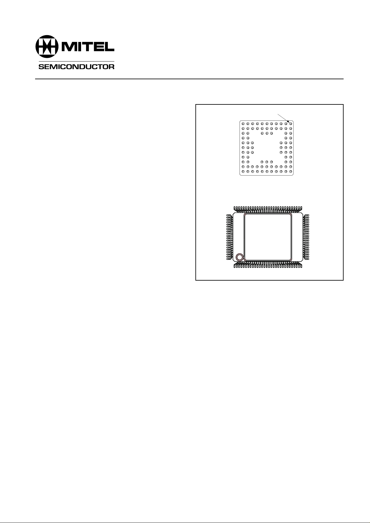
■ 84-pin Pin Grid Array or 84 Contact LCC Packages
or 100 pin Ceramic Quad Flat Pack
PIN 1A INDEX MARK
ON TOP SURFACE
A
B
C
D
E
F
G
H
J
K
L
1234567891011
AC84
GC100
Fig.1 Pin connections - bottom view
APPLICATIONS
■ Digital Signal Processing
■ Array Processing
■ Graphics
■ Database Addressing
■ High Speed Arithmetic Processors
ASSOCIATED PRODUCTS
PDSP16112 Complex Multiplier
PDSP16116 16 x 16 Complex Multiplier
PDSP16318 Complex Accumulator
PDSP16330 Pythagoras Processor
ORDERING INFORMATION
PDSP1601 MC GGCR 10MHz MIL883 Screened -
QFP package
PDSP1601A BO AC 20MHz Industrial - PGA
package
N.B Further details of the Military grade part are
available in a separate datasheet (DS3763)
1
Page 2
PDSP1601/PDSP1601A
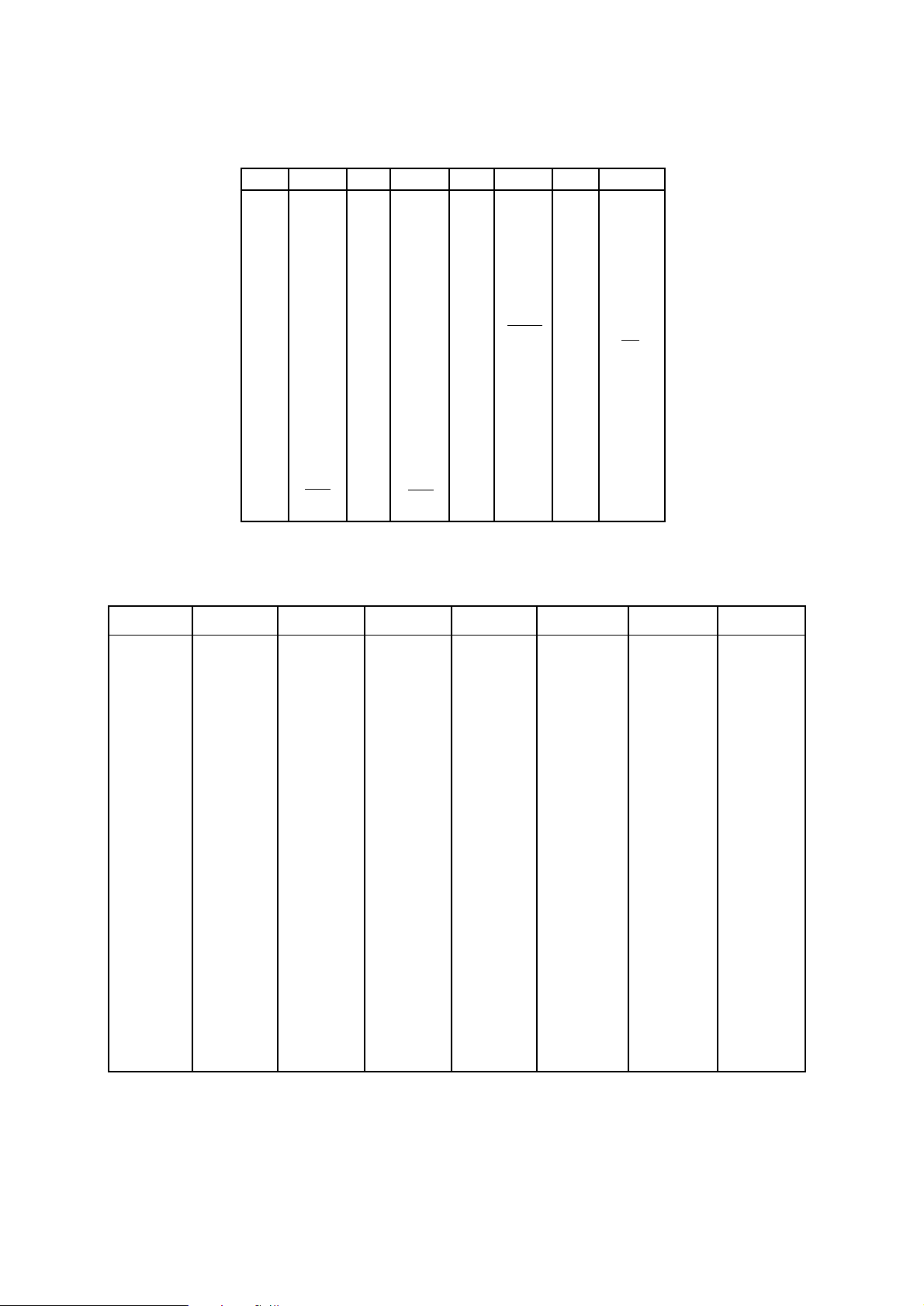
PIN DESCRIPTION
AC pin
C6
A6
A5
B5
C5
A4
B4
A3
A2
B3
A1
B2
C2
B1
C1
D2
D1
E3
E2
E1
F1
Function
IA4
MSB
MSS
B15
B14
B13
B12
B11
B10
B9
B8
B7
B6
B5
B4
B3
B2
B1
B0
CEB
CLK
AC pin
F3
G3
G1
G2
F1
H1
H2
J1
K1
J2
L1
K2
K3
L2
L3
K4
L4
J5
K5
L5
K6
Function
GND
MSA0
MSA1
A15
A14
A13
A12
A11
A10
A9
A8
A7
A6
A5
A4
A3
A2
A1
A0
CEA
MSC
AC pin
J6
J7
L7
K7
L6
L8
K8
L9
L10
K9
L11
K10
J10
K11
J11
H10
H11
F10
G10
G11
G9
Function
IS0
IS1
IS2
IS3
SV0
SV1
SV2
SV3
SVOE
RS0
RS1
VCC
RS2
C0
C1
C2
C3
C4
C5
C6
C7
AC pin
F9
F11
E11
E10
E9
D11
D10
C11
B11
C10
A11
B10
B9
A10
A9
B8
A8
B6
B7
A7
C7
Function
GND
C8
C9
C10
C11
C12
C13
C14
C15
OE
BFP
VCC
CO
RA0
RA1
RA2
CI
IA0
IA1
IA2
IA3
GC
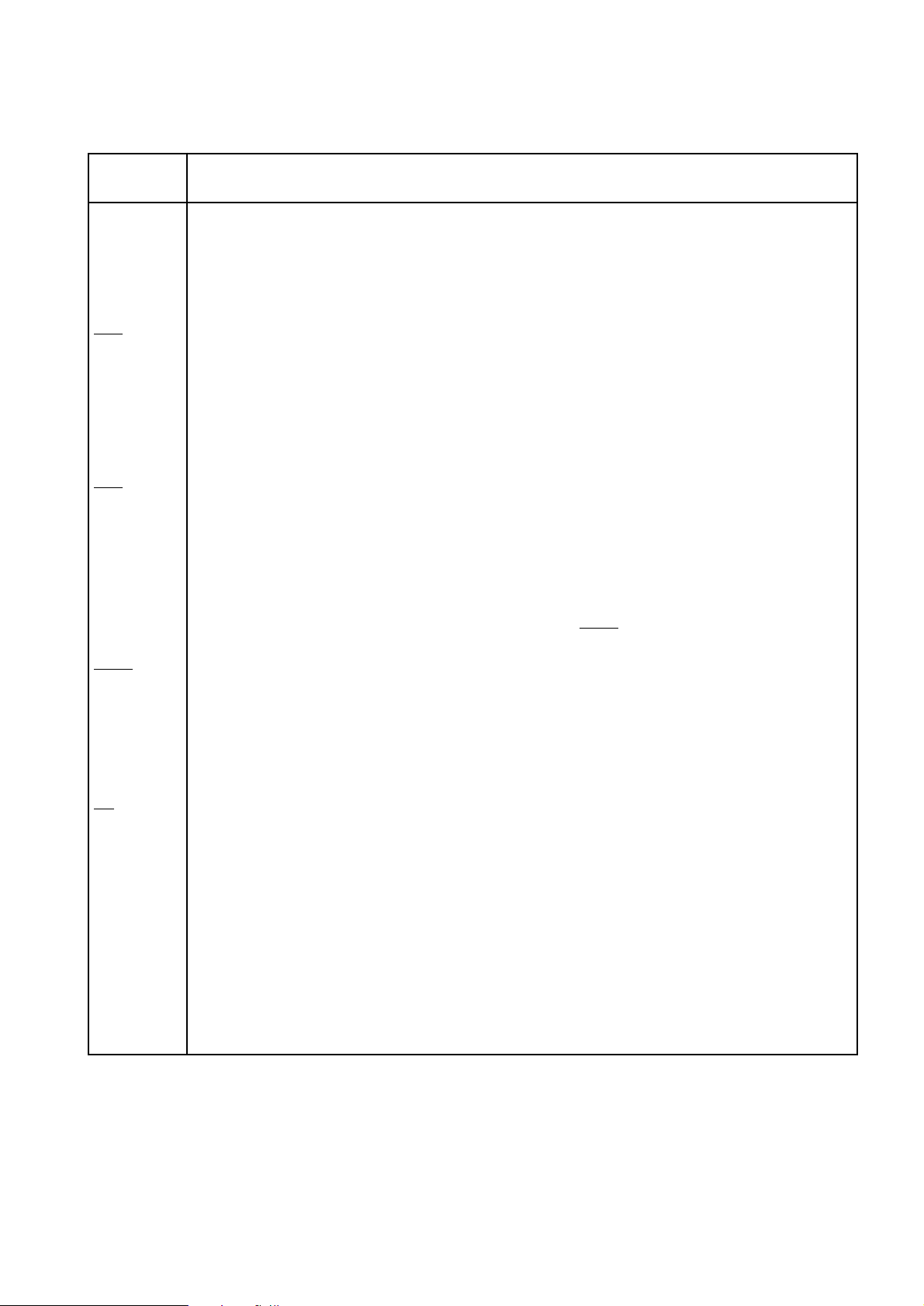
1
2
3
4
5
6
7
8
9
10
11
12
13
14
15
16
17
18
19
20
21
22
23
24
25
SIG
N/C
N/C
N/C
N/C
VCC
C0
RA0
RA1
RA2
CI
IA0
IA1
IA2
IA3
IA4
MSB
MSS
B15
B14
B13
B12
B11
B10
B9
B8
GC
26
27
28
29
30
31
32
33
34
35
36
37
38
39
40
41
42
43
44
45
46
47
48
49
50
SIG
N/C
N/C
N/C
N/C
B7
B6
B5
B4
B3
B2
B1
B0
CEB
CLK
GND
MSA0
MSA1
A15
A14
A13
A12
A11
A10
A9
A8
GC
51
52
53
54
55
56
57
58
59
60
61
62
63
64
65
66
67
68
69
70
71
72
73
74
75
SIG
N/C
N/C
N/C
N/C
A7
A6
A5
A4
A3
A2
A1
A0
CEA
MSC
IS0
IS1
IS2
IS3
SV0
SV1
SV2
SV3
SVOE
RS0
RS1
GC
76
77
78
79
80
81
82
83
84
85
86
87
88
89
90
91
92
93
94
95
96
97
98
99
100
SIG
N/C
N/C
N/C
N/C
VCC
RS2
C0
C1
C2
C3
C4
C5
C6
C7
GND
C8
C9
C10
C11
C12
C13
C14
C15
OE
BFP
N/C = not connected - leave open circuit
All GND and VDD pin must be used
2
Page 3
PIN DESCRIPTIONS
PDSP1601/PDSP1601A
Symbol
MSB
MSS
B15 - B0
CEB
CLK
MSA0 - MSA1
A15 - A0
CEA
MSC
IS0 - IS3
SV0 - SV3
Description
ALU B-input multiplexer select control.
1
This input is latched internally on the rising edge
of CLK.
Shifter Input multiplexer select control.1 This input is latched internally on the rising edge
of CLK.
B Port data input. Data presented to this port is latched into the input register on the rising
edge of CLK. B15 is the MSB.
Clock enable, B Port input register. When low the clock to this register is enabled.
Common clock to all internal registered elements. All registers are loaded, and outputs
change on the rising edge of CLK.
ALU A-input multiplexer select control.1 These inputs are latched internally on the rising
edge of CLK.
A Port data input. Data presented to this port is latched into the input register on the rising
edge of CLK. A15 is the MSB.
Clock enable, A Port input register. When low the clock to this register is enabled.
C-Port multiplexer select control.1 This input is latched internally on the rising edge
of CLK.
Instruction inputs to Barrel Shifter, IS3 = MSB.1 These inputs are latched internally on the
rising edge of CLK.
Shift Value I/O Port. This port is used as an input when shift values are supplied from
external sources, and as an output when Normalise operations are invoked. The I/O functions
are determined by the IS0 - IS3 instruction inputs, and by the
The shift value is latched internally on the rising edge of CLK.
SVOE control.
SVOE
SV Output enable. When high the SV port can only operate as an input. When low the SV
port can act as an input or as an output, according to the IS0 - IS3 instruction. This pin should
be tied hihg or low, depending upon the application.
RS0, RS1
RS2
C0 - C15
Instruction inputs to Barrel Shifter registers.
rising edge of CLK.
C Port data output. Data output on this port is selected by the C output multiplexer.
1
These inputs are latched internally on the
C15 is the MSB.
OE
BFP
CO
RA0 - RA2
Output enable. The C Port outputs are in high impedance condition when this control is high.
Block Floating Point Flag from ALU, active high.
Carry out from MSB of ALU.
Instruction inputs to ALU registers.1 These inputs are latched internally on the rising
edge of CLK.
CI
IA0 - IA3
IA4
Vcc
GND
Carry in to LSB of ALU.
Instruction inputs to ALU.1 IA4 = MSB. These inputs are latched internally on the rising
edge of CLK.
+5V supply: Both Vcc pins must be connected.
0V supply: Both GND pins must be connected.
NOTES
1. All instructions are executed in the cycle commencing with the rising edge of the CLK which latches the inputs.
3
Page 4
PDSP1601/PDSP1601A
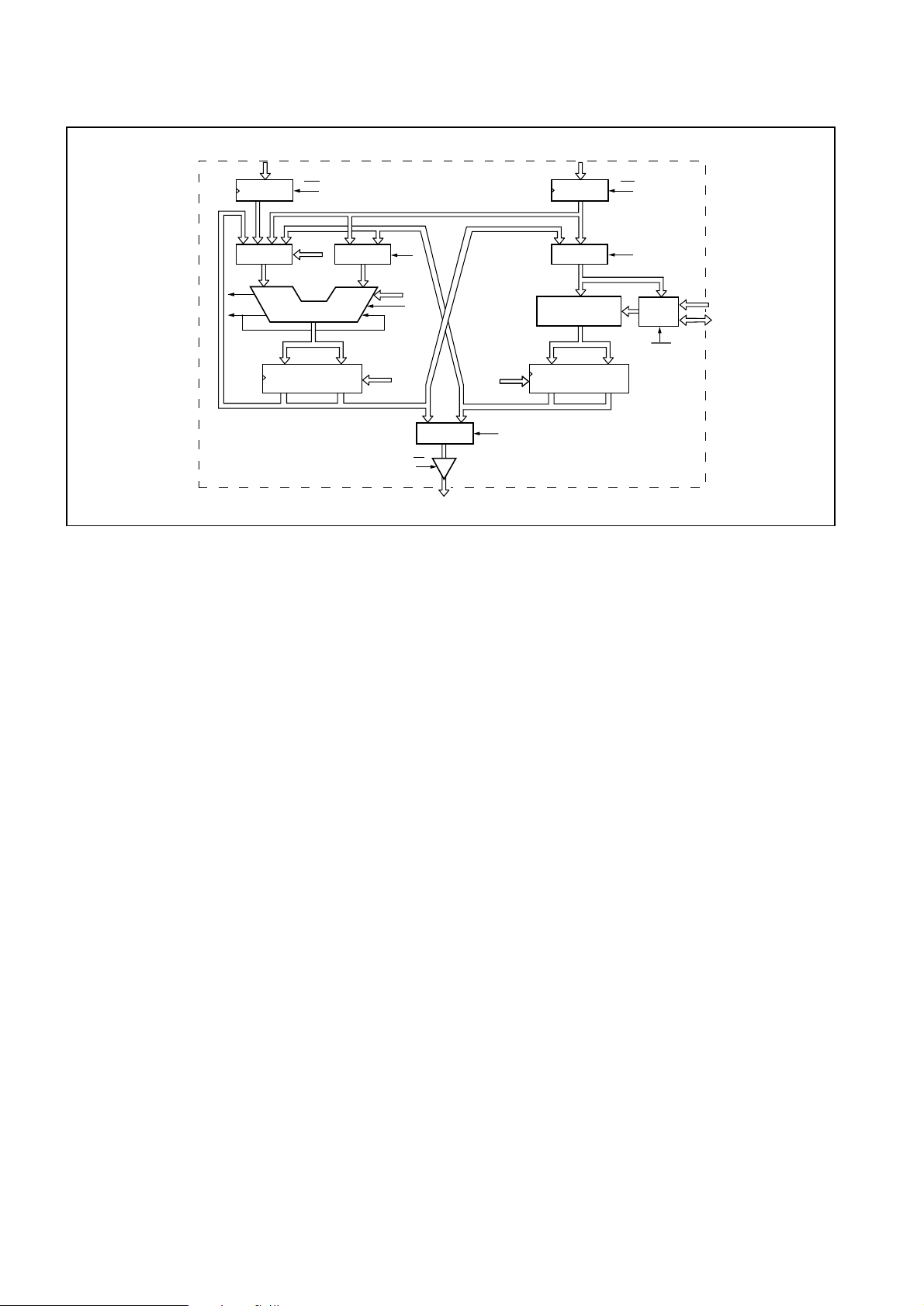
A INPUT
A REG
A MUX
BFP
AB
CO
LEFT REG. RIGHT REG.
FUNCTIONAL DESCRIPTION
16
ALU REG FILE
CEA
MSA0-1
ALU
RAD-2
IA0-4
MSB
5
CI
3
C MUX
OE
16
COUT
B MUX
2
Fig.2 PDSP1601 block diagram
MSC
RS0-2
3
LEFT REG. RIGHT REG.
B INPUT
16
B REG
S MUX
BARREL SHIFTER
SHIFTER REG FILE
CEB
MSS
SHIFT
CONTROL
SVOE
IS0-3
SV0-3
The PDSP1601 contains four main blocks: the ALU, the
Barrel Shifter and the two Register Files.
The ALU
The ALU supports 32 instructions as detailed in Table 1.
The inputs to the ALU are selected by the A and B MUXs.
Data will fall through from the selected register through the A
or B input MUXs and the ALU to the ALU output register file in
50ns for the PDSP1601A (100ns for the PDSP1601).
The ALU instructions are latched, such that the instruction
will not start executing until the rising edge of CLK latches the
instruction into the device.
The ALU accepts a carry in from the CI input and supplies
a carry out to the CO output. Additionally, at the end of each
cycle, the carry out from the ALU is loaded into an internal 1
bit register, so that it is available as an input to the ALU on the
next cycle. In the manner, multicycle, multiprecision
operations are supported. (See MULTICYCLE CASCADE
OPERATIONS).
BFP Flag
The ALU has a user programmable BFP flag. This flag
may be programmed to become active at any one of four
conditions. Two of these conditions are intended to support
Block Floating Point operations, in that they provide flags
indicating that the ALU result is within a factor of two or four of
overflowing the 16 bit number range. For multiprecision
operations the flag is only valid whilst the most significant 16
bit byte is being processed. In this manner the BFP flag may
be used over any extended word width.
The remaining two conditions detect either an overflow
condition or a zero result. For the overflow condition to be
active the ALU result must have overflowed into the 16th (sign)
bit, (this flag is only valid whilst the most significant 16 bit byte
is being processed). The zero condition is active if the result
from the ALU is equal to zero. For multiprecision operations
the zero flag must be active for all of the 16 bit bytes of an
extended word.
The BFP flag is programmed by executing on of the four
SBFXX instructions (see Table 1). During the execution of any
of these four instructions, the output of the ALU is forced to
zero.
Multicycle/Cascade Operation
The ALU arithmetic instructions contain two or three
options for each arithemtic operation.
The ALU is designed to operate with two's complement
arithmetic, requiring a one to be added to the LSB for all
subtract operations. The instructions set includes instructions
that will force a one into the LSB, e.g. MIAX1, AMBX1, BMAX1
(see Table 1).
These instructions are used for the least significant 16 bit
byte of any subtract operation.
The user has an option of cascading multiple devices, or
multicycling a single device to extend the arithmetic precision.
Should the user cascade multiple devices, then the cascade
arithmetic instructions using the external CI input should be
employed for all but the least significant 16 bit byte, e.g. MIACI,
APBCI, BMACI (see Table 1).
Should the user multicycle a single device, then the
Multicycle Arithmetic instructions, using the internally
registered CO bit should be employed for all but the least
significant 16 bit byte, e.g. MIACO, APBCO, AMBCO,
BMACO (see Table 1).
4
Page 5
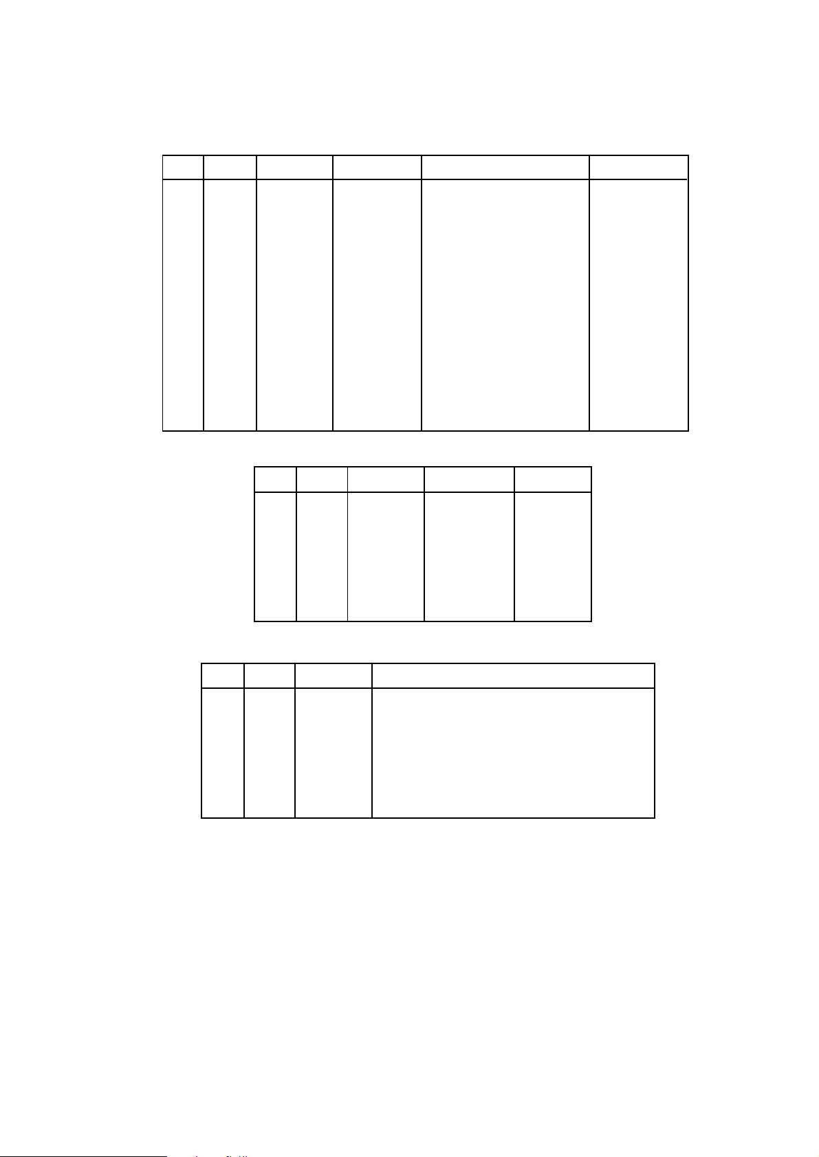
Table 1 ALU instructions
Inst
IA4-AI0
Mnemonic
1a. ARITHMETIC INSTRUCTIONS
Operation
Function
PDSP1601/PDSP1601A
Mode
00
01
02
03
04
05
06
07
08
09
0A
0B
0C
0D
0E
0F
00000
00001
00010
00011
00100
00101
00110
00111
01000
01001
01010
01011
01100
01101
01110
01111
CLRXX
MIAX1
MIACI
MIACO
A2SGN
A2RAL
A2RAR
A2RSX
APBCI
APBCO
AMBX1
AMBCI
AMBCO
BMAX1
BMACI
BMACO
Inst
10
11
12
13
14
15
16
17
RESET
MINUS A
MINUS A
MINUS A
A/2
A/2
A/2
A/2
A PLUS B
A PLUS B
A MINUS B
A MINUS B
A MINUS B
B MINUS A
B MINUS A
B MINUS A
1b. LOGICAL INSTRUCTIONS
IA4-AI0
10000
10001
10010
10011
10100
10101
10110
10111
Mnemonic
ANXAB
ANANB
ANNAB
ORXAB
ORNAB
XORAB
PASXA
PASNA
CLEAR ALL REGISTERS
NA Plus 1
NA Plus CI
NA Plus CO
A/2 Sign Extend
A/2 with RAL LSB
A/2 with RAR LSB
A/2 with RSX LSB
A Plus B Plus CI
A Plus B Plus CO
A Plus NB Plus 1
A Plus NB Plus CI
A Plus NB Plus CO
NA Plus B Plus 1
NA Plus B Plus CI
NA Plus B Plus CO
Operation
A AND B
A AND NB
NA AND B
A OR B
NA OR B
A XOR B
PASS A
INVERT A
Function
A. B
A. NB
NA. B
A + B
NA + B
A XOR B
A
NA
---------
LSBYTE
CASCADE
MULTICYCLE
MSBYTE
MULTICYCLE
MULTICYCLE
MULTICYCLE
CASCADE
MULTICYCLE
LSBYTE
CASCADE
MULTICYCLE
LSBYTE
CASCADE
MULTICYCLE
1c. CONTROL INSTRUCTIONS
Inst
18
19
1A
1B
1C
1D
1E
1F
IA4-AI0
11000
11001
11010
11011
11100
11101
11110
11111
Mnemonic
SBFOV
SBFU1
SBFU2
SBFZE
OPONE
OPBYT
OPNIB
OPALT
KEY
A = A input to ALU
B = B input to ALU
CI = External Carry in to ALU
CO = Internally Registered Carry out from ALU
RAL = ALU Register (Left)
RAR = ALU Register (Right)
RSX = Shifter Register (Left or Right)
Operation
Set BFP Flag to OVR, Force ALU output to zero
Set BFP Flag to UND 1 Force ALU output to zero
Set BFP Flag to UND 2 Force ALU output to zero
Set BFP Flag to ZERO Force ALU output to zero
Output 0001 Hex
Output 00FF Hex
Output 000F Hex
Output 5555 Hex
MNEMONICS
CLRXX Clear All Registers to zero
MIAXX Minus A, XX = Carry in to LSB
A2XXX A Divided by 2, XXX = Source of MSB
APBXX A Plus B, XX = Carry in to LSB
AMBXX A Minus B, XX = Carry in to LSB
BMAXX B Minus A, XX = Carry in to LSB
ANX-Y AND X = Operand 1, Y = Operand 2
ORX-Y OR X = Operand 1, Y = Operand 2
XORXY Exclusive OR X = Operand 1, Y = Operand 2
PASXX Pass XX = Operand
SBFXX Set BFP Flag XX = Function
OPXXX Output Constant XXX
5
Page 6
PDSP1601/PDSP1601A
Divide by Two
The Barrel Shifter
The ALU has four (A2SGN, A2RAL, A2RAR, A2RSX)
instructions used for right shifting (dividing by two) extended
precision words. These words, (up to 64 bits) may be stored
in the two on-chip register files. When the least significant 16
bit word is shifted, the vacant MSB must be filled with the LSB
from the next most significant 16 bit byte. This is achieved via
the A2RAL, A2RAR or A2RSX instructions which indicate the
source of the new MSB (see ALU INSTRUCTION SET).
When the most significant 16 bit byte is right shifted, the
MSB must be filled with a duplicate of the original MSB so as
to maintain the correct sign (Sign Extension). This operation
is achieved via the A2SGN instruction (see Table 1).
Constants
The ALU has four instructions (OPONE, OPBYT, OPNIB,
OPALT) that force a constant value onto the ALU output.
These values are primarily intended to be used as masks, or
the seeds for mask generation, for example, the OPONE
instruction will set a single bit in the least significant position.
This bit may be rotated any where in the 16 bit field by the
Barrel Shifter, allowing the AND function of the ALU to perform
bit-pick operations on input data.
CLR
The ALU instruction CLRXX is used as a Master Reset for
the entire device. This instruction has the effect of:
The Barrel Shifter supports 16 instructions as detailed in
Table 2. The input to the Barrel Shifter is selected by the S
MUX. Data will fall through from the selected register, through
the S MUX and the Barrel Shifter to the shifter output register
file in 50ns for the PDSP1601A (100ns for the PDSP1601).
The Barrel Shifter instructions are latched, such that the
instructions will not start executing until the rising edge of CLK
latches the instruction into the device.
The Barrel Shifter is capable of Logical Arithmetic or Barrel
Shifts in either direction.
A. Logical shifts discard bits that exit the 16 bit field and fill
spaces with zeros.
B. Arithmetic shifts discard bits that exit the 16 bit field and
fill spaces with duplicates of the original MSB.
C. Barrel Shifts rotate the 16 bit fields such that bits tha exit
the 16 bit field to the left or right reappear in the vacant
spaces on the right or left.
The amount of shift applied is encoded onto the 4 bit Barrel
Shifter input as illustrated in Table 3. The type of shift and the
amount are determined by the shift control block. The shift
control block (see Fig.3) accepts and decodes the four bit ISO3 instruction. The shift control block contains a priority
encoder and two user programmable 4 bit registers R1 and
R2.
There are four possible sources of shift value that can be
passed onto the Barrel Shifter, there are:
1. Clearing ALU and Barrel Shifter register files to zero.
2. Clearing A and B port input registers to zero.
3. Clearing the R1 and R2 shift control registers to zero.
4. Clearing the internally registered CO bit to zero.
5. Programming the BFP flag to detect
Inst
0
1
2
3
4
5
6
7
8
9
A
B
C
D
E
F
overflow
IS3-IS0
0000
0001
0010
0011
0100
0101
0110
0111
1000
1001
1010
1011
1100
1101
1110
1111
conditions.
Mnemonic
LSRSV
LSLSV
BSRSV
BSLSV
LSRR1
LSLR1
LSRR2
LSLR2
LR1SV
LR2SV
ASRSV
ASRR1
ASRR2
NRMXX
NRMR1
NRMR2
Table 2 Barrel shifter instructions
KEY
SV = Shift Value
R1 = Register 1
R2 = Register 2
PE = Priority Encoder Output
I => SV Port operates as an Input
O => SV Port operates as an Output
X => SV Port in a High Impedance State
6
1. The Priority Encoder
2. The SV input
3. The R1 register
4. The R2 register
Operation
Logical Shift Right by SV
Logical Shift Left by SV
Barrel Shift Right by SV
Barrel Shift Left by SV
Logical Shift Right by R1
Logical Shift Left by R1
Logical Shift Right by R2
Logical Shift Left by R2
Load Register 1 From SV
Load Register 2 From SV
Arithmetic Shift Right by SV
Arithmetic Shift Right by R1
Arithmetic Shift Right by R2
Normalise Output PE
Normalise Output PE, Load R1
Normalise Output PE, Load R2
MNEMONICS
LSXYY Logical Shift, X = Direction YY = Source of Shift Value
BSXYY Barrel Shift, X = Direction YY = Source of Shift Value
ASXYY Arithmetic Shift, X = Direction YY = Source of Shift Value
LXXYY Load XX = Target YY = Source
NRMYY Normalise by PE, Output PE value on SV Port, Load YY Reg
I/O
I
I
I
I
X
X
X
X
I
I
I
X
X
O
O
O
Page 7

PDSP1601/PDSP1601A
SV3
SV2
SV1
SV0
0
0
0
0
0
0
0
1
0
0
1
0
0
0
1
1
0
1
0
0
0
1
0
1
0
1
1
0
0
1
1
1
1
0
0
0
1
0
0
1
1
0
1
0
1
0
1
1
1
1
0
0
1
1
0
1
1
1
1
0
1
1
1
1
Shift
No shift
1 place
2 places
3 places
4 places
5 places
6 places
7 places
8 places
9 places
10 places
11 places
12 places
13 places
14 places
15 places
Table 3 Barrel shifter codes
Priority Encoder
If the priority encoder is selected as the source of the shift
value (instructions:- NRMXX, NRMR1, MRMRZ), then within
one 100ns cycle or two 50ns cycles for the PDSP1601A (one
200ns or two 100ns cycles for the PDSP1601), the shift
circuitry will:
(1) Priority encode the 16 bit input to the Barrel Shifter and
place the 4 bit value in either of the R1 or R2 registers and
output the value on the SV port (if enabled by
SVOE).
(2) Shift the 16 bit input by the amount indicated by the
Priority Encoder such that the output from the Barrel Shifter is
a normalised value.
SV Input
If the SV port is selected as the source of the shift value,
then the input to the Barrel Shifter is shifted by the value stored
in the internal SV register.
SVOESVOE
SVOE
SVOESVOE
The SV port acts as an input or an output depending upon
the IS0-3 instruction. If the user does not wish to use the
normalise instructions, then the SV port mat be forced to be
input only by typing SVOE control high. In this mode the SV
port may be considered an extension of the instruction inputs.
R1 and R2 Registers
The R1 and R2 registers may be loaded from the Priority
Encoder (NRMR1 and NRMR2) or from the SV input (LR1SV,
LR2SV).
Whilst the latter two instructions are executing, the Barrel
Shifter will pass its input to the output unshifted.
16
INSTRUCTION
PRIORITY ENCODER
4
MUX
MUX
R1
MUX
R2
DECODE
4
IS0-3
4
SV
SVOE
Fig.3 Shift control block
7
Page 8

PDSP1601/PDSP1601A
The Register Files
There are two on-chip register files (ALU and Shifter), each
containing two 16 bit registers and each supporting 8
instructions (see Table 4). The instructions for the ALU
register file and the Barrel Shifter Register file are the same.
The Inputs to the register files come from either the ALU or
the Barrel Shifter, and are loaded into the Register files on the
rising edge of CLK.
The register file instructions are latched such that the
instruction will not start executing until the rising edge of the
ALU REGISTER INSTRUCTIONS
Inst
0
1
2
3
4
5
6
7
Inst
RA2-RA0
000
001
010
011
100
101
110
111
RA2-RA0
Mnemonic
LLRRR
LRRLR
LLRLR
LRRRR
LBRLR
NOPRR
NOPLR
NOPPS
SHIFTER REGISTER INSTRUCTIONS
Mnemonic
Load Left Reg Output Right Reg
Load Right Reg Output Left Reg
Load Left Register, Output Left Reg
Load Right Register, Output Right Reg
Load Both Registers, Output Left Reg
No Load Operation, Output Right Reg
No Load Operation, Output Left Reg
No Load Operation, Pass ALU Result
CLK latches the instruction into the device.
The register file instructions (see Table 4) allow input data
to be loaded into either, neither or both of the registers. Data
is loaded at the end of the cycle in which the instruction is
executing.
The register file instructions allow the output to be sourced
from either of the two registers, the selected output will be valid
during the cycle in which the instruction is executing.
Operation
Operation
0
1
2
3
4
5
6
7
000
001
010
011
100
101
110
111
LLRRR
LRRLR
LLRLR
LRRRR
LBRLR
NOPRR
NOPLR
NOPPS
Load Left Reg Output Right Reg
Load Right Reg Output Left Reg
Load Left Register, Output Left Reg
Load Right Register, Output Right Reg
Load Both Registers, Output Left Reg
No Load Operation, Output Right Reg
No Load Operation, Output Left Reg
No Load Operation, Pass Barrel Shifter Result
Table 4 ALU and shift register instructions mnemonics
MNEMONICS
LXXYY Load XX = Target, YY = Source of Output
LBOXX Load Both Registers, XX = Source of Output
NOPXX No Load Operation, XX = Source of Output
8
Page 9

Multiplexers
PDSP1601/PDSP1601A
There are four user selectable on-chip multiplexers (A-
MUX, B-MUX, S-MUX and C-MUX).
These four multiplexers support instructions as tabulated
in Table 5.
MSA1
A-MUX
B-MUX
S-MUX
C-MUX
MARAX
MAAPR
MABPR
MARSX
0
0
1
1
MSB
0
1
MSS
0
1
MSC
0
1
MSA0
0
1
0
1
The MUX instructions are latched such that the instruction
will not start executing until the rising edge of CLK latches the
instruction onto the device.
Output
ALU REGISTER FILE OUPUT
A-PORT INPUT
B-PORT INPUT
SHIFTER REGISTER FILE OUTPUT
Output
B-PORT INPUT
SHIFTER REGISTER FILE OUTPUT
Output
B-PORT INPUT
SHIFTER REGISTER FILE OUTPUT
Output
ALU REGISTER FILE OUTPUT
SHIFTER REGISTER FILE OUTPUT
Table 5
9
Page 10

PDSP1601/PDSP1601A
INSTRUCTION SET
ALU Arithmetic Instructions
Mnemonic
CLRXX
Op Code
<00>
Function
On the rising edge of CLK at the end of the cycle in which this instruction is executing, the
A Port, B Port, ALU, Barrel Shifter, and Shift Control Registers will be loaded with zeros.
The internal registered CO will also be set to zero, and the BFP flag will be set to activate
on overflow conditions.
MIAX1
MIAC1
MIACO
A2SGN
A2RAL
A2RAR
A2RSX
APBCI
APBCO
AMBX1
AMBCI
AMBCO
BMAX1
BMAC1
<01>
<02>
<03>
<04>
<05>
<06>
<07>
<08>
<09>
<0A>
<0B>
<0C>
<0D>
<0E>
The A input to the ALU is inverted and a one is added to the LSB.
The A input to the ALU is inverted and the CI input is added to the LSB.
The A input to the ALU is inverted and the CO output from the ALU on the previous cycle
is added to the LSB.
The A input to the ALU is right shifted one bit position. The LSB is discarded, and the vacant
MSB is filled by duplicating the original MSB (Sign Extension).
The A input to the ALU is right shifted one bit position. The LSB is discarded, and the vacant
MSB is filled with the LSB from the ALU register.
The A input to the ALU is right shifted one bit position. The LSB is discarded, and the vacant
MSB is filled with the LSB from the ALU register.
The A input to the ALU is right shifted one bit position. The LSB is discarded, and the vacant
MSB is filled with the LSB from the B input to the ALU.
The A input to the ALU is added to the B input, and the CI input is added to the LSB.
The A input to the ALU is added to the B input, and the CO out from the ALU on the previous
cycle is added to the LSB.
The A input to the ALU is added to the inverted B input, and a one is added to the LSB.
The A input to the ALU is added to the inverted B input, and the CI input is added to the
LSB.
The A input to the ALU is added to the inverted B input, and the CO out from the ALU on
the previous cycle is added to the LSB.
The inverted A input to the ALU is added to the B input, and a one is added to the LSB.
The inverted A input to the ALU is added to the B input, and the CI input is added to the
LSB.
BMACO
ALU Logical Instructions
Mnemonic
ANXAB
ANANB
ANNAB
ORXAB
ORNAB
XORAB
PASXA
PASNA
<0F>
Op Code
<10>
<11>
<12>
<13>
<14>
<15>
<16>
<17>
10
The inverted A input to the ALU is added to the B input, and the CO out from the ALU on
the previous cycle is added to the LSB.
Function
The A input to the ALU is logically 'ANDed' with the B input.
The A input to the ALU is logically 'ANDed' with the inverse of the B input.
The inverse of the A input to the ALU is logically 'ANDed' with the B input.
The A input to the ALU is logically 'ORed' with the B input.
The inverse A input to the ALU is logically 'ORed' with the B input.
The A input to the ALU is logically Exclusive-ORed with the B input.
The A input to the ALU is passed to the output.
The inverse of the A input to the ALU is passed to the output.
Page 11

ALU Control Instructions
Mnemonic
SBFOV
Op Code
<18>
PDSP1601/PDSP1601A
Function
The BFP flag is programmed to activate when an ALU operation causes an overflow of the
16 bit number range. This flag is logically the exclusive-or of the carry into and out of the
MSB of the ALU. For the most significant Byte this flag indicates that the result of an
arithmetic two's complement operation has overflowed into the sign bit. The output of the
ALU is forced to zero for the duration of this instruction.
SBFU1
SBFU2
SBFZE
OPONE
OPBYT
OPNIB
OPALT
Barrel Shifter Instructions
Mnemonic
LSRSV
<19>
<1A>
<1B>
<1C>
<1D>
<1E>
<1F>
Op Code
<0>
The BFP flag is programmed to activate when an ALU operation comes within a factor of
two of causing an overflow of the 16 bit number range. For the most significant Byte this
flag indicates that the result of an arithmetic two's complement operation is within a factor
of two of overflowing into the sign bit. The output of the ALU is forced to zero for the duration
of this instruction.
The BFP flag is programmed to activate when an ALU operation comes within a factor of
four of causing an overflow of the 16 bit number range. For the most significant Byte this
flag indicates that the result of an arithmetic two's complement operation is within a factor
of four of overflowing into the sign bit. The output of the ALU is forced to zero for the duration
of this instruction.
The BFP flag is programmed to activate when an ALU operation causes a result of zero.
The output of the ALU is forced to zero for the duration of this instruction. During the
execution of this instruction the BFP flag will become active.
The ALU will output the binary value 0000000000000001, the MSB on the left.
The ALU will output the binary value 0000000011111111, the MSB on the left.
The ALU will output the binary value 0000000000001111, the MSB on the left.
The ALU will output the binary value 0101010101010101, the MSB on the left.
Function
The 16 bit input to the Barrel Shifter is right shifted by the number of places indicated by
the magnitude of the four bit number present in the SV register. The LSBs are dicarded,
and the vacant MSBs are filled with zeros.
LSLSV
BSRSV
BSLSV
LSRR1
LSLR1
LSRR2
LSLR2
<1>
<2>
<3>
<4>
<5>
<6>
<7>
The 16 bit input to the Barrel Shifter is left shifted by the number of places indicated by the
magnitude of the four bit number present in the SV register. The LSBs are dicarded, and
the vacant MSBs are filled with zeros.
The 16 bit input to the Barrel Shifter is rotated to the right by the number of places indicated
by the magnitude of the four bit number present in the SV register. The LSBs that exit the
16 bit field to the right, reappear in the vacant MSBs on the left.
The 16 bit input to the Barrel Shifter is rotated to the left by the number of places indicated
by the magnitude of the four bit number present in the SV register. The LSBs that exit the
16 bit field to the right, reappear in the vacant MSBs on the right.
The 16 bit input to the Barrel Shifter is right shifted by the number of places indicated by
the magnitude of the four bit number resident within the R1 register. The LSBs are
discarded, and the vacant MSBs are filled with zeros.
The 16 bit input to the Barrel Shifter is left shifted by the number of places indicated by the
magnitude of the four bit number resident within the R1 register. The LSBs are discarded,
and the vacant LSBs are filled with zeros.
The 16 bit input to the Barrel Shifter is right shifted by the number of places indicated by
the magnitude of the four bit number resident within the R2 register. The LSBs are
discarded, and the vacant MSBs are filled with zeros.
The 16 bit input to the Barrel Shifter is left shifted by the number of places indicated by the
magnitude of the four bit number resident within the R2 register. The LSBs are discarded,
and the vacant LSBs are filled with zeros.
11
Page 12

PDSP1601/PDSP1601A
Mnemonic
LR1SV
LR2SV
ASRSV
ASRR1
ASRR2
NRMXX
Op Code
<8>
<9>
<A>
<B>
<C>
<D>
Function
On the rising edge of CLK at the end of the cycle in which this instruction is executing, the
R1 register will be loaded with the data present on the SV port. The input to the Barrel
Shifter will be passed onto the output unshifted.
On the rising edge of CLK at the end of the cycle in which this instruction is executing, the
R2 register will be loaded with the data present on the SV port. The input to the Barrel
Shifter will be passed onto the output unshifted.
The 16 bit input to the Barrel Shifter is right shifted by the number of places indicated by
the magnitude of the four bit number present in the SV register. The LSBs are discarded,
and the vacant MSBs are filled with duplicates of the original MSB. (Sign Extension).
The 16 bit input to the Barrel Shifter is right shifted by the number of places indicated by
the magnitude of the four bit number resident within the R1 register. The LSBs are
discarded, and the vacant MSBs are filled with duplicates of the original MSB.
(Sign Extension).
The 16 bit input to the Barrel Shifter is right shifted by the number of places indicated by
the magnitude of the four bit number resident within the R2 register. The LSBs are
discarded, and the vacant MSBs are filled with duplicates of the original MSB.
(Sign Extension).
The 16 bit input to the Barrel Shifter is left shifted by the number of places indicated by the
magnitude of the four bit number output from the Priority Encoder. This value is also output
on the SV port (provided
The effect of this operation is to left shift the input by the necessary amount
(max 15 places) to result in the MSB and the next most significant bit being different. This
has the effect of eliminating unnecessary Sign Bits, and hence Normalising the input data.
The MSBs shifted out to the left are discarded, and the vacant LSBs on the right are filled
with zeros.
SVOE is low).
NRMR1
NRMR2
<E>
<F>
The 16 bit input to the Barrel Shifter is left shifted by the number of places indicated by the
magnitude of the four bit number output from the Priority Encoder. This value is also loaded
into the R1 register at the end of the cycle, and is output on the SV port (provided SVOE
is low).
The effect of this operation is to left shift the input by the necessary amount
(max 15 places) to result in the MSB and the next most significant bit being different. This
has the effect of eliminating unnecessary Sign Bits, and hence Normalising the input data.
The MSBs shifted out to the left are discarded, and the vacant LSBs on the right are filled
with zeros.
The 16 bit input to the Barrel Shifter is left shifted by the number of places indicated by the
magnitude of the four bit number output from the Priority Encoder. This value is also loaded
into the R2 register at the end of the cycle, and is output on the SV port (provided SVOE
is low).
The effect of this operation is to left shift the input by the necessary amount
(max 15 places) to result in the MSB and the next most significant bit being different. This
has the effect of eliminating unnecessary Sign Bits, and hence Normalising the input data.
The MSBs shifted out to the left are discarded, and the vacant LSBs on the right are filled
with zeros.
12
Page 13

Barrel Shifter or ALU Register Instructions
Mnemonic
LLRRR
Op Code
<0>
After the rising edge of CLK at the beginning of the cycle in which this instruction is
executed, the contents of the Right register will appear on the output. On the rising edge
of CLK at the end of the cycle, and the data on the register inputs will be loaded into the
Left Register.
PDSP1601/PDSP1601A
Function
LRRLR
LLRLR
LRRRR
LBRLR
NOPRR
NOPLR
NOPPS
<1>
<2>
<3>
<4>
<5>
<6>
<7>
After the rising edge of CLK at the beginning of the cycle in which this instruction is
executed, the contents of the Left register will appear on the output. On the rising edge
of CLK at the end of the cycle, the data on the register inputs will be loaded into the Right
Register.
After the rising edge of CLK at the beginning of the cycle in which this instruction is
executed, the contents of the Left register will appear on the output. On the rising edge
of CLK at the end of the cycle, the data on the register inputs will be loaded into the Left
Register.
After the rising edge of CLK at the beginning of the cycle in which this instruction is
executed, the contents of the Right register will appear on the output. On the rising edge
of CLK at the end of the cycle, the data on the register inputs will be loaded into the Right
Register.
After the rising edge of CLK at the beginning of the cycle in which this instruction is
executed, the contents of the Left register will appear on the output. On the rising edge
of CLK at the end of the cycle, and the data on the register inputs will be loaded into both
Left and Right Register.
After the rising edge of CLK at the beginning of the cycle in which this instruction is
executed, the contents of the Right register will appear on the output. On the rising edge
of CLK at the end of the cycle no load operation will occur, the register contents will remain
unchanged.
After the rising edge of CLK at the beginning of the cycle in which this instruction is
executed, the contents of the Left register will appear on the output. On the rising edge
of CLK at the end of the cycle no load operation will occur, the register contents will remain
unchanged.
After the rising edge of CLK at the beginning of the cycle in which this instruction is
executed, the input to the registers will appear on the output. On the rising edge
of CLK at the end of the cycle no load operation will occur, the register contents will remain
unchanged.
13
Page 14

PDSP1601/PDSP1601A
TYPICAL APPLICATION
Select a 16 bit field from each word in a block of 32 bit
words with a 10MHz throughput.
The 16 bit field indicated is to be selected from each 32 bit
word.
MS Byte LS Byte
MS Bit
8888
16 bits
nbits
The 32 bit words are fed into the B port of the PDSP1601
in two cycles, MS byte first.
The PDSP1601 shift control is initiated by programming
the R1 and R2 registers with n and 16-n respectively.
The shift operation is implemented in three steps:-
(1) The MS byte is logically left shifted (16-n) places, the
MSBs being discarded and the LSB spaces being filled with
zeros. This shifted data is loaded into the shifter register file
left register.
(2) The LS byte is logically right shifted, n-places, the
LSBs being discarded and the MSBs being filled with zeros.
This shifted data is loaded into the shifter register file left
register.
During this cycle the previous contents of this register are
passed through the ALU to the ALU register file left register.
(3) While the MS byte of the next 32 bit word is shifted in
the Barrel Shifter, the two previous results, resident within the
left registers of the ALU and Shifter Register files are 'ORed'
by the ALU, the result being the desired 16 bit field is loaded
into the ALU register file right register ready to be output on the
next cycle.
The instructions from initialisation are given in Table 6.
CLK
1/
2/
3/
4/
5/
6/
7/
8/
CEB
1
1
0
0
0
0
0
0
MSA
MARSX
MARSX
MARSX
MARSX
MARSX
MARAX
MARSX
MARAX
MSB
1
1
1
1
1
1
1
1
MSS
0
0
0
0
0
0
0
0
MSC
0
0
0
0
0
0
0
0
IA
CLRXX
PASXA
PASXA
PASXA
PASXA
ORXAB
PASXA
ORXAB
IS
X
LR1SV
LR2SV
LSLR2
LSRR1
LSLR2
LSRR1
LSLR2
Repeat instruction pair 5/ and 6/ until all 16 bit fields have been selected.
Table 6
ABSOLUTE MAXIMUM RATINGS (Note 1)
Supply voltage Vcc -0.5V to 7.0V
Input voltage V
Output voltage V
Clamp diode current per pin Ik (see note 2) ±18mA
IN
OUT
-0.9 to Vcc + 0.9V
-0.9 to Vcc + 0.9V
Static discharge voltage (HMB) 500V
Storage temperature T
Ambient temperature with
power applied T
Military -40°C to +125°C
Industrial -40°C to +85°C
S
amb
-65°C to +150°C
Package power dissipation PTOT
AC 1000mw
LC 1000mw
NOTES
1. Exceeding these ratings may cause permanent damage.
Functional operation under these conditions is not implied.
2. Maximum dissipation or 1 second should not be exceeded, only
one output to be tested at any one time.
THERMAL CHARACTERISTICS
Package type ΘJC °C/W ΘJA °C/W
AC 12 36
GC 12 35
SV
X
n
(16-n)
X
X
X
X
X
RA
NOPLR
NOPLR
NOPLR
NOPLR
LLRRR
LRRLR
LLRRR
LRRLR
RS
NOPLR
NOPLR
NOPLR
LLRLR
LLRLR
LLRLR
LLRLR
LLRLR
Comment
Clear
Load R1 with n
Load R2 with (16-n)
Shift 1st MS byte
Shift 1st LS byte
OR 1st bytes and
shift 2nd MS byte
Shift 2nd LS byte
and output first result
Shift 3rd LS byte
14
Page 15

ELECTRICAL CHARACTERISTICS
Operating Conditions (unless otherwise stated)
T
(Commercial) = 0°C to +70°C, VCC = 5.0V±5%, Ground = 0V
AMB
T
(Industrial) = -40°C to +85°C, VCC = 5.0V±10%, Ground = 0V
AMB
T
(Military) = -55°C to +125°C, VCC = 5.0V±10%, Ground = 0V
AMB
Static Characteristics
Characteristic
Symbol
Min.
Value
Typ.
Max.
Units
PDSP1601/PDSP1601A
Conditions
Output high voltage
Output low voltage
Input high voltage
Input low voltage
Input leakage current
Vcc current
Output leakage current
Output S/C current
Input capacitance
V
OH
V
OL
V
IH
V
IL
I
IL
I
CC
I
OZ
I
SC
C
IN
2.4
3.5
-10
-50
12
5
Switching Characteristics
Characteristic
CLK rising edge to C-PORT
CLK rising edge to CO
CLK rising edge to BFP
Setup CEA or CEB to CLK rising edge
CEA or CEB after CLK rising edge
Hold
Setup A or B port inputs to CLK rising edge
Hold A or B port inputs after CLK rising edge
Setup MSA0-1, MSB, MSS, MSC, RA2-0, RS0-2, IA0-4,
IS0-3, to CLK rising edge
Hold RS0-2, IA0-4 after CLK rising edge
Hold IS0-3 after CLK rising edge
Hold MSA0-1, MSB, MSS, MSC, RA0-2 after CLK rising edge
Setup SV to CLK rising edge
Hold SV after CLK rising edge
CLK rising edge to SV
OE
C-PORT Z
OE
C-PORT Z
OE
C-PORT Z
OE
C-PORT Z
Clock period (ALU & Barrel Shifter, serial mode)
Clock period (ALU & Barrel Shifter, parallel mode)
Clock high time
Clock low time
NOTES 1. LSTTL is equivalent to IOH at 20µA IOL of -0.4mA
2. Current is defined as negative into the device.
PDSP1601
Min.
5
5
5
30
40
40
40
5
200
100
40
40
0.4
0.5
+10
60
+50
80
Value
Max.
40
100
100
0
0
0
3
0
3
100
40
40
40
40
V
V
V
V
µA
mA
µA
mA
pF
PDSP1601A
Min.
Max.
5
25
5
50
5
50
15
0
20
0
20
0
3
0
20
3
5
50
25
25
25
25
100
50
20
20
IOH = 8mA
IOL = -8mA
GND < VIN < V
T
= -40°C to +85°C
amb
GND < V
VCC = Max
Units
ns
ns
ns
< V
OUT
Conditions
2 x LSTTL + 20pF
1 x LSTTL + 5pF
1 x LSTTL + 5pF
ns
ns
ns
ns
ns
ns
ns
ns
Input mode
ns
Input mode
ns
20pF load, SV O P mode
ns
2 x LSTTL + 20pF
ns
2 x LSTTL + 20pF
ns
2 x LSTTL + 20pF
ns
2 x LSTTL + 20pF
ns
ns
ns
ns
ns
CC
CC
15
Page 16

Page 17

http://www.mitelsemi.com
World Headquarters - Canada
Tel: +1 (613) 592 2122
Fax: +1 (613) 592 6909
North America Asia/Pacific Europe, Middle East,
Tel: +1 (770) 486 0194 Tel: +65 333 6193 and Africa (EMEA)
Fax: +1 (770) 631 8213 Fax: +65 333 6192 Tel: +44 (0) 1793 518528
Fax: +44 (0) 1793 518581
Information relating to products and services furnished herein by Mitel Corporation or its subsidiaries (collectively “Mitel”) is believed to be reliable. However, Mitel assumes no
liability for errors that may appear in this publication, or for liability otherwise arising from the application or use of any such information, product or service or for any infringement of
patents or other intellectual property rights owned by third parties which may result from such application or use. Neither the supply of such information or purchase of product or
service conveys any license, either express or implied, under patents or other intellectual property rights owned by Mitel or licensed from third parties by Mitel, whatsoever.
Purchasers of products are also hereby notified that the use of product in certain ways or in combination with Mitel, or non-Mitel furnished goods or services may infringe patents or
other intellectual property rights owned by Mitel.
This publication is issued to provide information only and (unless agreed by Mitel in writing) may not be used, applied or reproduced for any purpose nor form par t of any order or
contract nor to be regarded as a representation relating to the products or services concerned. The products, their specifications, services and other information appearing in this
publication are subject to change by Mitel without notice. No warranty or guarantee express or implied is made regarding the capability, performance or suitability of any product or
service. Information concerning possible methods of use is provided as a guide only and does not constitute any guarantee that such methods of use will be satisfactory in a specific
piece of equipment. It is the user’s responsibility to fully determine the performance and suitability of any equipment using such information and to ensure that any publication or
data used is up to date and has not been superseded. Manufacturing does not necessarily include testing of all functions or parameters. These products are not suitable for use in
any medical products whose failure to perform may result in significant injury or death to the user. All products and materials are sold and services provided subject to Mitel’s
conditions of sale which are available on request.
M Mitel (design) and ST-BUS are registered trademarks of MITEL Corporation
Mitel Semiconductor is an ISO 9001 Registered Company
Copyright 1999 MITEL Corporation
All Rights Reserved
Printed in CANADA
TECHNICAL DOCUMENTATION - NOT FOR RESALE
 Loading...