

Page 1

查询PDIUSBP11供应商
INTEGRATED CIRCUITS
PDIUSBP11
Universal Serial Bus transceiver
Product specification 1997 Sep 16
Page 2
Philips Semiconductors Preliminary specification
,
VMO
PDIUSBP1 1Universal Serial Bus transceiver
FEA TURES
•Utilizes digital inputs and outputs to transmit and receive USB
cable data
•Supports 12Mbit/s “Full Speed” and 1.5Mbit/s “Low Speed” serial
data transmission
•Compatible with the VHDL “Serial Interface Engine” from USB
developer’s conference
•Available in SO, 14 pin package
•Hysteresis on D+, D–, V
MO
inputs
DESCRIPTION
The PDIUSBP11 is a one chip generic USB transceiver. It is
designed to allow 5.0V or 3.3V programmable and standard logic to
interface with the physical layer of the Universal Serial Bus. It is
capable of transmitting and receiving serial data at both full speed
(12Mbit/s) and low speed (1.5Mbit/s) data rates. The outputs from
the serial interface engine (inputs VPO and VMO on the
PDIUSBP11) are driven by the host. The gated inputs (outputs VP
and VM on the PDIUSBP11) are to be decoded by the host.
Implementation of the Serial Interface Engine along with the USB
transceiver allow the designer to make flexible USB compatible
devices with widely available logic components.
ORDERING INFORMATION
PACKAGES TEMPERATURE RANGE OUTSIDE NORTH AMERICA NORTH AMERICA PKG. DWG. #
14-pin plastic SO 0°C to +70°C PDIUSBP11 D PDIUSBP11 D SOT108-1
14-pin plastic SSOP 0°C to +70°C PDIUSBP11 DB PDIUSBP11 DB SOT337-1
14-pin plastic TSSOP 0°C to +70°C PDIUSBP11 PW PDUSBP11 PW DH SOT402-1
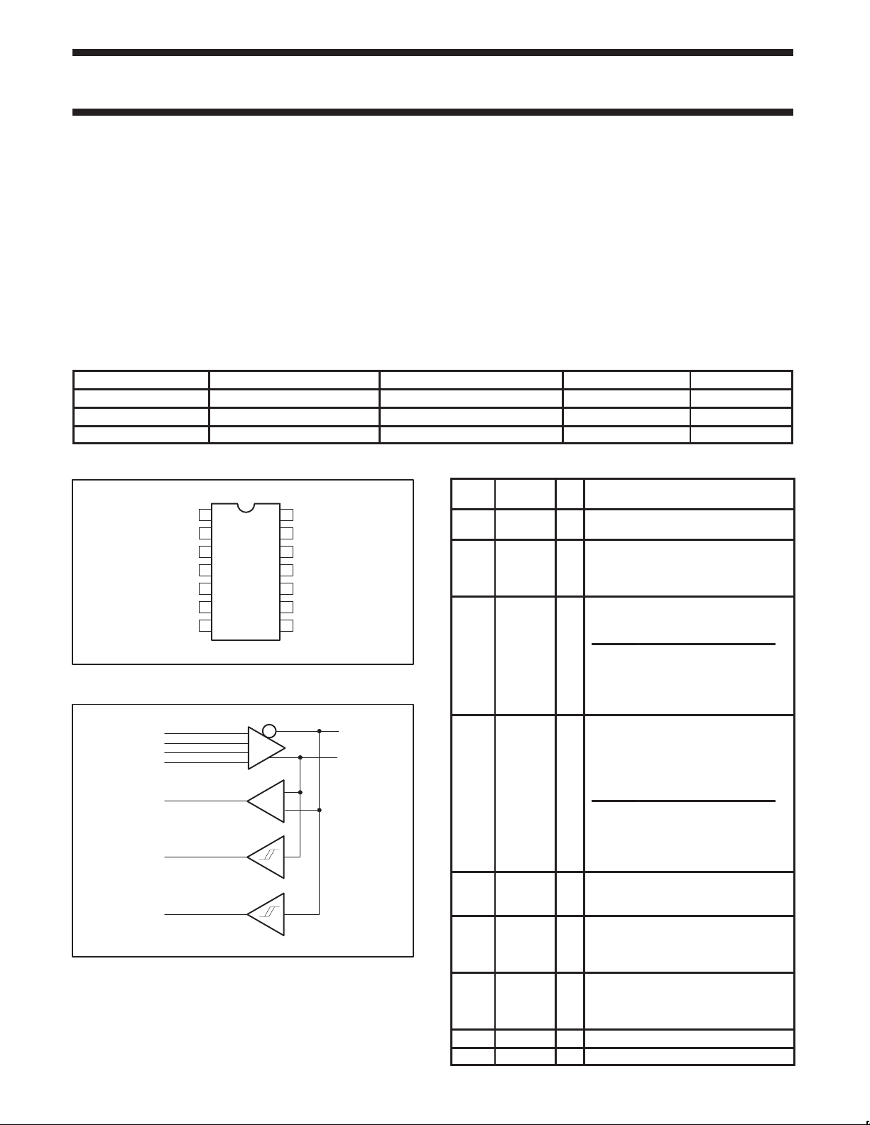
PIN CONFIGURATION
1
NC
2
OE#
3
RCV
4
VP
5
VM
SUSPND
6
7
GND NC
FUNCTIONAL DIAGRAM
OE#
SPEED
VMO
VPO
RCV
VP
VM
14
V
CC
13
VMO
12
VPO
11
D
10
D–
9
SPEED
8
SV00142
D–
D+
+
–
SV00143
PIN DESCRIPTION
PIN
No.
3 RCV O
2 OE# I
12, 13
4, 5 VP, VM O
11, 10 D+, D– I/O
6 SUSPND I
9 SPEED I
14 V
7 GND Ground reference
PIN
SYMBOL
VPO,
CC
I/O NAME AND FUNCTION
Receive data. CMOS level output for
USB differential input
Output Enable. Active LOW, enables
the transceiver to transmit data on
the bus. When not active the
transceiver is in receive mode
Inputs to differential driver . (Outputs
from SIE).
VPO VMO RESULT
I
0 0 SE0
0 1 Logic “0”
1 0 Logic “1”
1 1 Undefined
Gated version of D– and D+. Outputs
are logic “0” and logic “1”. Used to
detect single ended zero (SE0#),
error conditions, and interconnect
speed. (Inputs to SIE).
VP VM RESULT
0 0 SE0
0 1 Low Speed
1 0 Full Speed
1 1 Error
Data+, Data–. Differential data bus
conforming to the Universal Serial
Bus standard.
Suspend. Enables a low power state
while the USB bus is inactive. While
the suspnd pin is active it will drive
the RCV pin to a logic “0” state.
Edge rate control. Logic “1” operates
at edge rates for “full speed”. Logic
“0” operates edge rates for “low
speed”.
3.0V to 3.6V power supply
1997 Sep 16 853-1836 18389
2
Page 3

Philips Semiconductors Preliminary specification
SYMBOL
PARAMETER
CONDITIONS
UNIT
MIN.MAX
SYMBOL
PARAMETER
CONDITIONS
UNIT
PDIUSBP11Universal Serial Bus transceiver
RECOMMENDED OPERATING CONDITIONS
LIMITS
.
T
V
V
CC
V
I/O
V
amb
DC supply voltage 3.0 3.6 V
DC Input voltage range 0 5.5 V
I
DC input range for I/O’s 0 V
DC output voltage range 0 V
O
Operating ambient temperature range in
free air
See DC and AC characteristics
for individual device
0 +70 °C
CC
CC
V
V
ABSOLUTE MAXIMUM RATINGS
1, 2
In accordance with the Absolute Maximum Rating System (IEC 134) Voltages are referenced to GND (ground = 0V)
LIMITS
MIN MAX
I
GND
V
I
V
I
V
T
P
DC supply voltage –0.5 +6.5 V
CC
DC input diode current VI < 0 – –50 mA
IK
V
DC input voltage Note 3 –0.5 +5.5 V
I
DC input voltage range for I/O’s –0.5 V
I/O
DC output diode current VO > VCC or VO < 0 – "50 mA
OK
DC output voltage Note 3 –0.5 VCC +0.5 V
O
DC output source or sink current for VP/VM,
I
O
RCV pins
DC output source or sink current for D+/D–
I
O
pins
VO = 0 to V
VO = 0 to V
CC
CC
– "15 mA
– "50 mA
+0.5 V
CC
, ICCDC VCC or GND current – "100 mA
Storage temperature range –60 +150 °C
stg
Power dissipation per package mW
tot
NOTES:
1. Stresses beyond those listed may cause permanent damage to the device. These are stress ratings only and functional operation of the
device at these or any other conditions beyond those indicated under “recommended operating conditions” is not implied. Exposure to
absolute-maximum-rated conditions for extended periods may affect device reliability .
2. The performance capability of a high-performance integrated circuit in conjunction with its thermal environment can create junction
temperatures which are detrimental to reliability. The maximum junction temperature of this integrated circuit should not exceed 150°C.
3. The input and output voltage ratings may be exceeded if the input and output clamp current ratings are observed.
1997 Sep 16
3
Page 4

Philips Semiconductors Preliminary specification
3
3
1
ns
2
ns
1
ns
2
ns
D+/D– to RCV
3
ns
D+/D– to VP/VM
1
ns
4
ns
PDIUSBP11Universal Serial Bus transceiver
DC ELECTRICAL CHARACTERISTICS
Over recommended operating conditions
Voltages are referenced to GND (ground = 0V)
LIMITS
SYMBOL
V
IH
V
HIGH level input VCC = 3.0V to 3.6V
LOW level input VCC = 3.0V to 3.6V
IL
RD H Output impedance (HIGH state) Note 2 28 34 43 Ω
RD L Output impedance (LOW state) Note 2 28 35 51 Ω
V
OH
V
I
CCQ
I
CCS
I
CCFS
I
CCLS
I
OZ
OL
I
HIGH level output
LOW level output
Quiescent supply current VCC = 3.6V; VI = VCC or GND; IO = 0 330 600 µA
Supply current in Suspend VCC = 3.6V; VI = VCC or GND; IO = 0 – 65 µA
Active supply current (Full Speed) VCC = 3.3V 10 30 mA
Active supply current (Low Speed) VCC = 3.3V 2 25 mA
I
3-State output OFF-state current VI = VIH or VIL; VO = VCC or GND
NOTES:
1. All typical values are at V
2. This value includes an external resistor of 24Ω "1%. See “Load D+ and D–” diagram for testing details.
3. All signals except D+ and D–.
PARAMETER
TEST CONDITIONS Temp = 0°C to +70°C UNIT
MIN TYP1MAX
3
3
2.0 V
0.8 V
VCC = 3.0V; IO = 6mA 2.2 2.7
VCC = 3.0V; IO = 4mA 2.4
VCC = 3.0V; IO = 100µA 2.8 –
VCC = 3.0V; IO = 6mA 0.3 0.8
VCC = 3.0V; IO = 4mA 0.5
VCC = 3.0V; IO = 100µA – 0.2
Input leakage current VCC = 3.6V; VI = 5.5V or GND; not for I/O pins "0.1 "5 µA
= 3.3V and T
CC
amb
2
= 25°C.
"10 µA
V
V
AC CHARACTERISTICS
GND = 0V, tR = tF = 3.0ns, CL = 50pF, RL = 500Ω, VCC = 3.3V
LIMITS
SYMBOL PARAMETER TEST CONDITIONS WAVEFORMS
T
= 25°C T
amb
= 0°C to +70°C
amb
MIN TYP MAX MIN MAX
tp
LH
VMO/VPO to D+/D–
tp
t
t
tp
tp
t
t
tp
tp
tp
tp
tp
tp
tp
tp
t
V
Full Speed
HL
rise
Rise and Fall Times
Full Speed
fall
LH
VMO/VPO to D+/D–
Low Speed
HL
rise
Rise and Fall Times
Low Speed
fall
LH
HL
LH
HL
HZ
ZH
OE# to D+/D–
RL = 500Ω
LZ
ZL
Setup for SPEED 5 0 ns
su
Crossover point Note 1 3 1.3 2.0 1.3 2.0 V
cr
0 12 0 15
0 12 0 15
4 20 4 20
4 20 4 20
30 300 30 300
30 300 30 300
75 300 75 300
75 200 75 200
16 16
16 20
8 8
8 12
12 12
12 15
10 10
10 15
NOTE:
1. The crossover point is in the range of 1.3V to 2.5V for the low speed mode with a 50pF capacitance. In the low-speed mode with a 100pF or
greater capacitance, the crossover point is in the range of 1.3V to 2.0V .
UNIT
1997 Sep 16
4
Page 5

Philips Semiconductors Preliminary specification
PDIUSBP11Universal Serial Bus transceiver
AC WAVEFORMS
VM = 1.5V
= VOL +0.3V
V
X
= VOH –0.3V
V
Y
and VOH are the typical output voltage drops that occur with the
V
OL
output load. (V
never goes below 3.0V).
CC
2.7V
INPUT
GND
V
OH
V
OL
V
M
t
PLH
V
M
t
PHL
50%50%OUTPUT
SV00144
Waveform 1. D+/D– to VP/VM or VPO/VMO to D+/D–
t
RISE
V
OH
V
OL
10% 10%
t
FALL
90%90%
SV00186
Waveform 2. Rise and Fall Times
D+
V
CR
D–
V
OH
V
OL
t
PLH
V
M
V
t
PHL
2.0V
CR
1.0V
V
CR
2.7V
GND
SPEED
2.7V
GND
D.U.T.
V = 0 for t
V = VCC for t
1.5V 1.5V
t
su
V
M
t
Waveform 5. Setup for Speed
Test Point
D.U.T.
Load for VM/VP and RCV
Test Point
24Ω 500Ω
50pF
, t
PZH
PHZ
, t
PZL
PLZ
su
V
CR
SV00147
25pF
SV00149
V
+
–
2.7V
0V
OE#
V
OH
V
OL
D+/D–
1997 Sep 16
Waveform 3. D+/D– to RCV
1.5V 1.5V
t
t
PHZ
PLZ
0.5V
t
PZH
t
PZL
V
M
CC
Waveform 4. OE# to D+/D–
SV00146
SV00150
Load for Enable and Disable Times
Test Point
24Ω
D.U.T.
15kΩ
V
Y
0.5V
V
X
CC
C
= 50pF, Full Speed
L
C
= 50pF, Low Speed (Min Timing)
L
= 350pF, Low Speed (Max Timing)
C
L
* 1.5KΩ on D– (Low Speed) or D+ (Full Speed) Only
C
L
SV00187
1.5kΩ*S1
Test S1
D–/LS
D+/LS
D–/FS
D+/FS
SV00151
V
close
open
open
close
CC
Load for D+/D–
5
Page 6

Philips Semiconductors Product specification
PDIUSBP1 1Universal Serial Bus transceiver
SO14: plastic small outline package; 14 leads; body width 3.9 mm SOT108-1
1997 Sep 16
6
Page 7

Philips Semiconductors Product specification
PDIUSBP1 1Universal Serial Bus transceiver
SSOP14: plastic shrink small outline package; 14 leads; body width 5.3 mm SOT337-1
1997 Sep 16
7
Page 8

Philips Semiconductors Product specification
PDIUSBP1 1Universal Serial Bus transceiver
TSSOP14: plastic thin shrink small outline package; 14 leads; body width 4.4 mm SOT402-1
1997 Sep 16
8
Page 9

Philips Semiconductors Product specification
PDIUSBP1 1Universal Serial Bus transceiver
NOTES
1997 Sep 16
9
Page 10

Philips Semiconductors Product specification
PDIUSBP1 1Universal Serial Bus transceiver
DEFINITIONS
Data Sheet Identification Product Status Definition
Objective Specification
Preliminary Specification
Product Specification
Formative or in Design
Preproduction Product
Full Production
Philips Semiconductors and Philips Electronics North America Corporation reserve the right to make changes, without notice, in the products,
including circuits, standard cells, and/or software, described or contained herein in order to improve design and/or performance. Philips
Semiconductors assumes no responsibility or liability for the use of any of these products, conveys no license or title under any patent, copyright,
or mask work right to these products, and makes no representations or warranties that these products are free from patent, copyright, or mask
work right infringement, unless otherwise specified. Applications that are described herein for any of these products are for illustrative purposes
only. Philips Semiconductors makes no representation or warranty that such applications will be suitable for the specified use without further testing
or modification.
LIFE SUPPORT APPLICA TIONS
Philips Semiconductors and Philips Electronics North America Corporation Products are not designed for use in life support appliances, devices,
or systems where malfunction of a Philips Semiconductors and Philips Electronics North America Corporation Product can reasonably be expected
to result in a personal injury. Philips Semiconductors and Philips Electronics North America Corporation customers using or selling Philips
Semiconductors and Philips Electronics North America Corporation Products for use in such applications do so at their own risk and agree to fully
indemnify Philips Semiconductors and Philips Electronics North America Corporation for any damages resulting from such improper use or sale.
Philips Semiconductors
811 East Arques Avenue
P.O. Box 3409
Sunnyvale, California 94088–3409
Telephone 800-234-7381
This data sheet contains the design target or goal specifications for product development. Specifications
may change in any manner without notice.
This data sheet contains preliminary data, and supplementary data will be published at a later date. Philips
Semiconductors reserves the right to make changes at any time without notice in order to improve design
and supply the best possible product.
This data sheet contains Final Specifications. Philips Semiconductors reserves the right to make changes
at any time without notice, in order to improve design and supply the best possible product.
Philips Semiconductors and Philips Electronics North America Corporation
register eligible circuits under the Semiconductor Chip Protection Act.
Copyright Philips Electronics North America Corporation 1997
All rights reserved. Printed in U.S.A.
 Loading...