

Page 1

PDIUSBH11
Universal Serial Bus hub
Preliminary specification 1996 Nov 12
INTEGRATED CIRCUITS
Page 2
Philips Semiconductors Preliminary specification
PDIUSBH11Universal Serial Bus hub
2
1996 Nov 12
FEATURES
•Complies with the Universal Serial Bus specification Rev. 1.0
•Four downstream ports with per packet connectivity
•Embedded function with two endpoints (control and interrupt)
•Integrated FIFO memory for hub and embedded function
•Automatic protocol handling
•Versatile I
2
C interface
•Compliant with USB Human Interface and Display Device Class
•Single 3.3V supply and SDIP32 package
DESCRIPTION
The Philips Semiconductors Universal Serial Bus (USB) hub is
designed to provide USB expandability in a PC system and
plug-and-play control of the embedded function, for example,
monitor. The PDIUSBH11 is used in a microcontroller based system
and communicates with the system microcontroller over the I
2
C
serial bus.
This modular approach to implementing a hub and embedded
function allows the designer to either use a low cost dedicated
microcontroller or adapt the existing system microcontroller. The
PDIUSBH11 conforms to the USB specification 1.0 and the I
2
C
serial interface specification.
Since the device is a compound USB device (hub function plus
embedded function), the embedded function appears as PORT1 to
the host system. The four expansion ports are numbered 2 through
5.
ORDERING INFORMATION
PACKAGES TEMPERATURE RANGE OUTSIDE NORTH AMERICA NORTH AMERICA PKG. DWG. #
32-pin plastic SO 0°C to +70°C PDIUSBH11 D PDIUSBH11 D SOT287–1
32-pin plastic SDIP 0°C to +70°C PDIUSBH11 NB PDIUSBH11 NB SOT232–1
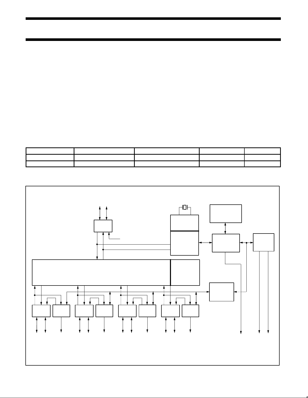
BLOCK DIAGRAM
ANALOG
TX/R
X
PORT
CONTROL
ANALOG
TX/R
X
PORT
CONTROL
ANALOG
TX/R
X
PORT
CONTROL
ANALOG
TX/R
X
PORT
CONTROL
GENERAL
PORT
CONTROLLER
HUB
REPEATER
END OF
FRAME
TIMERS
ANALOG
T
X/RX
PHILIPS
SIE
INTEGRATED
RAM
BIT CLOCK
RECOVERY
MEMORY
MANAGEMENT
UNIT
I
2
C
SLAVE
INTERFACE
48 MHz
FULL SPEED
INTERRUPT SDA SCL
LED
ENABLE
D–D+
LED
ENABLE
D–D+
LED
ENABLE
D–D+
LED
ENABLE
D–D+
DOWNSTREAM
PORT 2
DOWNSTREAM
PORT 3
DOWNSTREAM
PORT 4
DOWNSTREAM
PORT 5
D+
D–
UPSTREAM
PORT
SV00226
NOTE:
1. This is a conceptual block diagram and does not include each individual signal.
Page 3

Philips Semiconductors Preliminary specification
PDIUSBH11Universal Serial Bus hub
1996 Nov 12
3
Analog Transceivers
These transceivers interface directly to the USB cables through
some termination resistors. They are capable of transmitting and
receiving serial data at both “full speed” (12 Mbit/s) and “low speed”
(1.5 Mbit/s) data rates.
Hub Repeater
The hub repeater is responsible for managing connectivity on a per
packet basis. It implements packet signaling connectivity and
resume connectivity.
Low speed devices can be connected to downstream ports since the
repeater will not propagate upstream packets to downstream ports,
to which low speed devices are connected, unless they are
preceded by a PREAMBLE PID.
End of Frame Timers
This block contains the specified EOF1 and EOF2 timers which are
used to detect loss–of–activity and babble error conditions in the
hub repeater. The timers also maintain the low–speed keep–alive
strobe which is sent at the beginning of a frame.
General and Individual Port Controller
The general and individual port controllers together provide status
and control of individual downstream ports. Via the I
2
C–interface a
microcontroller can access the downstream ports and request or
change the status of each individual port.
Any change in the status or settings of the individual port will result
in an interrupt request. Via an interrupt register, the servicing
microcontroller can look up the downstream port which generated
the interrupt and request its new status. Any port status change can
then be reported to the host via the hub status change (interrupt)
endpoint.
Bit Clock Recovery
The bit clock recovery circuit recovers the clock from the incoming
USB data stream using (4X) over–sampling principle. It is able to
track jitter and frequency drift specified by the USB spec.
Philips Serial Interface Engine (PSIE)
The Philips SIE implements the full USB protocol layer. It is
completely hardwired for speed and needs no firmware intervention.
The functions of this block include: synchronisation pattern
recognition, parallel / serial conversion, bit stuffing / destuffing, CRC
checking / generation, PID verification / generation, address
recognition, handshake evaluation / generation.
Memory Management Unit (MMU) and Integrated RAM
The MMU and the integrated RAM is used to handle the large
difference in data–rate between USB, running in burst of 12 Mbit/s
and the I
2
C interface to the microcontroller, running at 100 kbit/s.
This allows the microcontroller to read and write USB packets at its
own (low) speed through I
2
C.
I
2
C Slave Interface
This block implements the necessary I
2
C interface protocol. A slave
I
2
C allows for simple micro–coding. An interrupt is used to alert the
microcontroller whenever the PDIUSBH11 needs attention. As a
slave I
2
C device, the PDIUSBH11 I2C clock: SCL is an input and is
controlled by the microcontroller.
Page 4

Philips Semiconductors Preliminary specification
PDIUSBH11Universal Serial Bus hub
1996 Nov 12
4
ENDPOINT DESCRIPTIONS
The following table summarizes the endpoints supported by the PDIUSBH11.
FUNCTION
ENDPOINT
NUMBER
ENDPOINT TYPE TRANSFER TYPE DIRECTION
MAXIMUM PACKET SIZE
(bytes)
0 Default Control IN, OUT 8
HUB
1 Status change Interrupt IN 1
0 Default Control IN, OUT 8
1 Interrupt Interrupt IN 8
PIN DESCRIPTION
The PDIUSBH11 has two modes of operation. The first mode
(Mode 0) enables the pins DNx_EN_N to power a LED indicating
the port is enabled. The second mode (Mode 1) utilizes the LED
enable pins as per port overcurrent condition pins.
The voltage level at power up on the TEST1 and TEST2 pins
determine the PDIUSBH11 mode of operation. When both of the
pins are connected to Ground, Mode 0 is enabled. When pins
TEST1 and TEST2 are connected to Vcc, Mode 1 is enabled. Note
that in Mode 1 the pin DN2_EN_N remains an LED enable pin. Pin
TEST3 should always be connected to Ground at all times.
PIN DESCRIPTION (MODE 0)
PIN NO PIN SYMBOL I/O DRIVE NAME AND FUNCTION
1 TEST1 I Connect to Ground
2 TEST2 I Connect to Ground
3 TEST3 I Connect to Ground
4 RESET_N I ST Power-on reset
5 GND POWER Ground reference
6 XTAL1 I Crystal connection 1 (48MHz)
7 XTAL2 O Crystal connection 2 (48MHz)
8 CLK12MHZ O 2mA 12MHz output clock for external devices
9 V
CC
POWER Voltage supply 3.3V 0.3V
10 OCURRENT_N I ST Over-current notice to the device
11 SWITCH_N O OD8 Enables power to downstream ports
12 SUSPEND O 4mA Device is in suspended state
13 DN2_EN_N O OD8 Downstream port 2 LED enable indicator
14 DN3_EN_N O OD8 Downstream port 3 LED enable indicator
15 DN4_EN_N O OD8 Downstream port 4 LED enable indicator
16 DN5_EN_N O OD8 Downstream port 5 LED enable indicator
17 INT_N O OD4 Connect to microcontroller interrupt
18 SDA I/O OD4 I2C bi-directional data
19 SCL I/O OD4 I2C bit-clock
20 GND POWER Ground reference
21 DN5_DP AI/O Downstream port 5 D+ connection
22 DN5_DM AI/O Downstream port 5 D– connection
23 DN4_DP AI/O Downstream port 4 D+ connection
24 DN4_DM AI/O Downstream port 4 D– connection
25 DN3_DP AI/O Downstream port 3 D+ connection
26 DN3_DM AI/O Downstream port 3 D– connection
27 DN2_DP AI/O Downstream port 2 D+ connection
28 DN2_DM AI/O Downstream port 2 D– connection
29 AGND POWER Analog Ground reference
30 AV
CC
POWER Analog voltage supply 3.3V 0.3V
31 UP_DP AI/O Upstream D+ connection
32 UP_DM AI/O Upstream D– connection
EMBEDDED
Page 5

Philips Semiconductors Preliminary specification
PDIUSBH11Universal Serial Bus hub
1996 Nov 12
5
PIN DESCRIPTION (MODE 1)
PIN NO PIN SYMBOL I/O DRIVE NAME AND FUNCTION
1 TEST1 I Connect to V
CC
2 TEST2 I Connect to V
CC
3 TEST3 I Connect to Ground
4 RESET_N I ST Power-on reset
5 GND POWER Ground reference
6 XTAL1 I Crystal connection 1 (48MHz)
7 XTAL2 O Crystal connection 2 (48MHz)
8 CLK12MHZ O 2mA 12MHz output clock for external devices
9 V
CC
POWER Voltage supply 3.3V 0.3V
10 OCURRENT2_N I ST Downstream port 2 over-current notice
11 SWITCH_N O OD8 Enables power to downstream ports
12 SUSPEND O 4mA Device is in suspended state
13 DN2_EN_N O OD8 Downstream port 2 LED enable indicator
14 OCURRENT3_N I ST Downstream port 3 over-current notice
15 OCURRENT4_N I ST Downstream port 4 over-current notice
16 OCURRENT5_N I ST Downstream port 5 over-current notice
17 INT_N O OD4 Connect to microcontroller interrupt
18 SDA I/O OD4 I2C bi-directional data
19 SCL I/O OD4 I2C bit-clock
20 GND POWER Ground reference
21 DN5_DP AI/O Downstream port 5 D+ connection
22 DN5_DM AI/O Downstream port 5 D– connection
23 DN4_DP AI/O Downstream port 4 D+ connection
24 DN4_DM AI/O Downstream port 4 D– connection
25 DN3_DP AI/O Downstream port 3 D+ connection
26 DN3_DM AI/O Downstream port 3 D– connection
27 DN2_DP AI/O Downstream port 2 D+ connection
28 DN2_DM AI/O Downstream port 2 D– connection
29 AGND POWER Analog Ground reference
30 AV
CC
POWER Analog voltage supply 3.3V 0.3V
31 UP_DP AI/O Upstream D+ connection
32 UP_DM AI/O Upstream D– connection
NOTES:
1. Signals ending in _N indicate active low signals.
ST: Schmitt Trigger
OD4, OD8: Open Drain with 4 or 8 mA drive
AI/O: Analog I/O
Page 6

Philips Semiconductors Preliminary specification
PDIUSBH11Universal Serial Bus hub
1996 Nov 12
6
RECOMMENDED OPERATING CONDITIONS
LIMITS
SYMBOL
PARAMETER
CONDITIONS
UNIT
MIN.
MAX.
V
CC
DC supply voltage 3.0 3.6 V
V
I
DC Input voltage range 0 5.5 V
V
I/O
DC input range for I/O 0 5.5 V
V
AI/O
DC input range for analog I/O 0 V
CC
V
V
O
DC output voltage range 0 V
CC
V
T
amb
Operating ambient temperature range in
free air
See DC and AC characteristics
for individual device
0 +70 °C
ABSOLUTE MAXIMUM RATINGS
1
In accordance with the Absolute Maximum Rating System (IEC 134) Voltages are referenced to GND (ground = 0V)
LIMITS
SYMBOL
PARAMETER
CONDITIONS
MIN MAX
UNIT
V
CC
DC supply voltage –0.5 +4.6 V
I
IK
DC input diode current VI < 0 – –50 mA
V
I
DC input voltage Note 2 –0.5 +5.5 V
V
I/O
DC input voltage range for I/O’s –0.5 V
CC
+0.5 V
I
OK
DC output diode current VO > VCC or VO < 0 – 50 mA
V
O
DC output voltage Note 2 –0.5 VCC +0.5 V
I
O
DC output source or sink current for VP/VM,
RCV pins
VO = 0 to V
CC
– 15 mA
I
O
DC output source or sink current for D+/D–
pins
VO = 0 to V
CC
– 50 mA
I
GND
, ICCDC VCC or GND current – 100 mA
T
stg
Storage temperature range –60 +150 °C
P
tot
Power dissipation per package mW
NOTES:
1. Stresses beyond those listed may cause permanent damage to the device. These are stress ratings only and functional operation of the
device at these or any other conditions beyond those indicated under “recommended operating conditions” is not implied. Exposure to
absolute-maximum-rated conditions for extended periods may affect device reliability.
2. The input and output voltage ratings may be exceeded if the input and output clamp current ratings are observed.
Page 7

Philips Semiconductors Preliminary specification
PDIUSBH11Universal Serial Bus hub
1996 Nov 12
7
DC ELECTRICAL CHARACTERISTICS (DIGITAL PINS)
LIMITS
SYMBOL
PARAMETER
TEST CONDITIONS Temp = 0°C to +70°C UNIT
MIN TYP MAX
Input Levels:
V
IH
HIGH level input voltage 0.9 V
V
IL
LOW level input voltage 2.5 V
VTLH LOW to HIGH threshold voltage ST (Schmitt Trigger) pins 80 %V
CC
VTHL HIGH to LOW threshold voltage ST (Schmitt Trigger) pins 20 %V
CC
VHYS Hysteresis voltage ST (Schmitt Trigger) pins 1.1 V
Output Levels:
I
OL
= rated drive 0.4
VOHHIGH level output
IOL = 20µA 0.1
V
I
OH
= rated drive VCC –0.4
VOLLOW level output
IOH = 20µA VCC –0.1
V
Leakage Current:
I
CCS
Supply current in Suspend Oscillator stopped 100 µA
I
I
Input leakage current
1 µA
I
OZ
3-State output OFF-state current OD (Open Drain) pins 5 µA
DC ELECTRICAL CHARACTERISTICS (AI/O PINS)
LIMITS
SYMBOL
PARAMETER
TEST CONDITIONS Temp = 0°C to +70°C UNIT
MIN MAX
Leakage Current:
I
LO
Hi–Z state data line leakage 0V < VIN < 3.3V 10 µA
Input Levels:
VDI Differential input sensitivity |(D+) – (D–)|
1
0.2 V
VCM Differential common mode range Includes VDI range 0.8 2.5 V
VSE Single ended receiver threshold 0.8 2.0 V
Output Levels:
V
OL
Static output LOW
RL of 1.5K to 3.6V
0.3 V
V
OH
Static output HIGH
RL of 1.5K to GND
2.8 3.6 V
Capacitance:
C
IN
Transceiver capacitance
Pin to GND 20 pF
Output Resistance:
ZDRV
2
Driver output resistance Steady state drive 28 43
NOTES:
1. D+ is the generic symbol for the USB positive data pins: UP_DP, DN2_DP, DN3_DP, DN4_DP, DN5_DP. D– is the generic symbol for the
USB negative data pins: UP_DM, DN2_DM, DN3_DM, DN4_DM, DN5_DM.
2. Includes external resistors of 24 1% each on D+ and D–.
Page 8

Philips Semiconductors Preliminary specification
PDIUSBH11Universal Serial Bus hub
1996 Nov 12
8
LOAD FOR D+/D–
D. U. T.
V
CC
TEST POINT
S1
C
L
CL = 50pF, FULL SPEED
C
L
= 50 pF, LOW SPEED (MIN TIMING)
C
L
= 350pF, LOW SPEED (MAX TIMING)
* 1.5K OHM ON D– (LOW SPEED) OR D+ (FULL SPEED) ONLY
TEST
S1
D–/LS
D+/LS
D–/FS
D+/FS
CLOSE
OPEN
OPEN
CLOSE
24 OHM
1.5K OHM*
SV00237
Page 9

Philips Semiconductors Preliminary specification
PDIUSBH11Universal Serial Bus hub
1996 Nov 12
9
APPLICATION DIAGRAM
I2C
ENABLE LED
POWER SWITCH
AND
OVERCURRENT CIRCUIT
5V
SWITCHED
5V
H11
µC
12MHz
48MHz
USB
DOWNSTREAM
USB
UPSTREAM
3.3V
SV00227
I2C Interface.
The I
2
C bus is used to interface to an external micro–controller
needed to control the operation of the hub. For cost consideration,
the target system microcontroller can be shared and utilized for this
purpose. The PDIUSBH11 implements a slave I
2
C interface. When
the PDIUSBH11 needs to communicate with the microcontroller it
asserts an interrupt signal. The microcontroller services this
interrupt by reading the appropriate status register on the
PDIUSBH11 through the I
2
C bus. (For more information about the
I
2
C serial bus, refer to I2C handbook. Philips order number 9397
750 00013).
The I
2
C interface on the PDIUSBH11 defines two types of
transactions :
1. command transaction
A command transaction is used to define which data (ex. status
byte, buffer data, ...) will be read from / written to the USB
interface in the next data transaction. A data transaction usually
follows a command transaction.
2. data transaction
A data transaction reads data from / writes data to the USB
interface. The meaning of the data is dependent on the
command transaction which was sent before the data
transaction.
Two addresses are used to differentiate between command and
data transactions. Writing to the command address is interpreted as
a command, while reading from / writing to the data address is used
to transfer data between the PDIUSBH11 and the controller
ADDRESS TABLE
TYPE OF ADDRESS
PHYSICAL ADDRESS
(MSB to LSB)
Command 0011 011 (binary)
Data 0011 010 (binary)
Protocol
An I
2
C transaction starts with a ‘Start Condition’, followed by an
address. When the address matches either the command or data
address the transaction starts and runs until a ‘Stop Condition’ or
another ‘Start Condition’ (repeated start) occurs.
The command address is write–only and is unable to do a read. The
next bytes in the message are interpreted as commands. Several
command bytes can be sent after one command address. Each of
the command bytes is acknowledged and passed on to the Memory
Management Unit inside the PDIUSBH11.
When the start condition address matches the data address, the
next bytes are interpreted as data. When the RW bit in the address
indicates a ‘master writes data to slave’ (=‘0’) the bytes are received,
acknowledged and passed on to the Memory Management Unit. If
the RW bit in the address indicates a ‘master reads data from slave’
(=‘1’) the PDIUSBH11 will send data to the master. The I
2
C–master
must acknowledge all data bytes except the last one. In this way the
I
2
C interface knows when the last byte has been transmitted and it
then releases the SDA line so that the master controller can
generate the STOP condition.
Repeated start support allows another packet to be sent without
generating a Stop Condition.
Timing
When the master writes data to the PDIUSBH11, the data is
sampled 1 micro–second after the rising edge of SCL. When the
PDIUSBH11 writes data to the master, the data is driven 1
micro–second after the falling edge of SCL.
Page 10

Philips Semiconductors Preliminary specification
PDIUSBH11Universal Serial Bus hub
1996 Nov 12
10
COMMAND SUMMARY
Some commands have the same command code (e.g., Read Buffer and Write Buffer). In these cases, the direction of the Data Phase (read or
write) indicates which command is executed.
COMMAND NAME
RECIPIENT CODING DATA PHASE
Initialization Commands
Set Address / Enable Hub D0h Write 1 byte
Embedded Function D1h Write 1 byte
Set Endpoint Enable Hub + Embedded Function D8h Write 1 byte
Data Flow Commands
Read Intereupt Register F4h Read 1 byte
Read Endpoint Status Hub Control OUT 40h Read 1 byte
Hub Control IN 41h Read 1 byte
Embedded Function Control OUT 42h Read 1 byte
Embedded Function Control IN 43h Read 1 byte
Embedded Function Interrupt 44h Read 1 byte
Select Endpoint Hub Control OUT 00h Read 1 byte (optional)
Hub Control IN 01h Read 1 byte (optional)
Embedded Function Control OUT 02h Read 1 byte (optional)
Embedded Function Control IN 03h Read 1 byte (optional)
Embedded Function Interrupt 04h Read 1 byte (optional)
Read Buffer Selected Endpoint F0h Read n bytes
Write Buffer Selected Endpoint F0h Write n bytes
Set Endpoint Status Hub Control OUT 40h Write 1 byte
Hub Control IN 41h Write 1 byte
Embedded Function Control OUT 42h Write 1 byte
Embedded Function Control IN 43h Write 1 byte
Embedded Function Interrupt 44h Write 1 byte
Acknowledge Setup Selected Endpoint F1h None
Clear Buffer Selected Endpoint F2h None
Validate Buffer Selected Endpoint FAh None
Hub Commands
Clear Port Feature Port 2 E0h Write 1 byte
Port 3 E1h Write 1 byte
Port 4 E2h Write 1 byte
Port 5 E3h Write 1 byte
Set Port Feature Port 2 E8h Write 1 byte
Port 3 E9h Write 1 byte
Port 4 EAh Write 1 byte
Port 5 EBh Write 1 byte
Get Port Status Port 2 E0h Read 1 or 2 bytes
Port 3 E1h Read 1 or 2 bytes
Port 4 E2h Read 1 or 2 bytes
Port 5 E3h Read 1 or 2 bytes
Set Status Change Bits E7h Write 1 byte
General Commands
Send Resume F6h None
Read Current Frame Number F5h Read 1 or 2 bytes
Page 11

Philips Semiconductors Preliminary specification
PDIUSBH11Universal Serial Bus hub
1996 Nov 12
11
SO32: plastic small outline package; 32 leads; body width 7.5mm SOT287-1
Page 12

Philips Semiconductors Preliminary specification
PDIUSBH11Universal Serial Bus hub
1996 Nov 12
12
SDIP32: plastic shrink dual in-line package; 32 leads (400 mil) SOT232-1
Page 13

Philips Semiconductors Preliminary specification
PDIUSBH11Universal Serial Bus hub
1996 Nov 12
13
NOTES
Page 14

Philips Semiconductors Preliminary specification
PDIUSBH11Universal Serial Bus hub
Philips Semiconductors and Philips Electronics North America Corporation reserve the right to make changes, without notice, in the products,
including circuits, standard cells, and/or software, described or contained herein in order to improve design and/or performance. Philips
Semiconductors assumes no responsibility or liability for the use of any of these products, conveys no license or title under any patent, copyright,
or mask work right to these products, and makes no representations or warranties that these products are free from patent, copyright, or mask
work right infringement, unless otherwise specified. Applications that are described herein for any of these products are for illustrative purposes
only. Philips Semiconductors makes no representation or warranty that such applications will be suitable for the specified use without further testing
or modification.
LIFE SUPPORT APPLICATIONS
Philips Semiconductors and Philips Electronics North America Corporation Products are not designed for use in life support appliances, devices,
or systems where malfunction of a Philips Semiconductors and Philips Electronics North America Corporation Product can reasonably be expected
to result in a personal injury. Philips Semiconductors and Philips Electronics North America Corporation customers using or selling Philips
Semiconductors and Philips Electronics North America Corporation Products for use in such applications do so at their own risk and agree to fully
indemnify Philips Semiconductors and Philips Electronics North America Corporation for any damages resulting from such improper use or sale.
This data sheet contains preliminary data, and supplementary data will be published at a later date. Philips
Semiconductors reserves the right to make changes at any time without notice in order to improve design
and supply the best possible product.
Philips Semiconductors
811 East Arques Avenue
P.O. Box 3409
Sunnyvale, California 94088–3409
Telephone 800-234-7381
DEFINITIONS
Data Sheet Identification Product Status Definition
Objective Specification
Preliminary Specification
Product Specification
Formative or in Design
Preproduction Product
Full Production
This data sheet contains the design target or goal specifications for product development. Specifications
may change in any manner without notice.
This data sheet contains Final Specifications. Philips Semiconductors reserves the right to make changes
at any time without notice, in order to improve design and supply the best possible product.
Philips Semiconductors and Philips Electronics North America Corporation
register eligible circuits under the Semiconductor Chip Protection Act.
Copyright Philips Electronics North America Corporation 1996
All rights reserved. Printed in U.S.A.
Date of release: 10–96
Document order number: 9397 750 01428
 Loading...