

Page 1

PDI1394L11
1394 AV link layer controller
Preliminary specification 1996 Nov 06
INTEGRATED CIRCUITS
Page 2

Philips Semiconductors Preliminary specification
PDI1394L111394 AV link layer controller
2
1996 Nov 06
1.0 FEATURES
•IEEE 1394–1995 Standard Link Layer Controller
•Hardware Support for the Proposed IEC1883 Standard of Digital
Interface for Consumer Electronics
•Interfaces to any IEEE 1394–1995 Physical Layer Interfaces
•5V Tolerant I/Os
•Single 3.3V supply voltage
2.0 DESCRIPTION
The PDI1394L11, Philips Semiconductors 1394 Audio/Video (AV)
Link Layer Controller, is an IEEE 1394–1995 compliant link layer
controller featuring an embedded AV layer interface. The AV layer is
designed to pack and un–pack application data packets for
transmission over an IEEE 1394 bus using isochronous data
transfers.
The application data is packetized according to the proposed IEC
1883 Specification of Digital Interface for Consumer Electronic
Audio/Video Equipment. The AV layer interface is a byte–wide port
capable of accommodating various MPEG–2 and DVC codecs. An
80C51 or MC68XX compatible byte–wide host interface is provided
for internal register configuration as well as performing
asynchronous data transfers.
The PDI1394L11 is powered by a single 3.3V power supply and the
inputs and outputs are 5V tolerant. It is available in the PQFP80
package.
3.0 QUICK REFERENCE DATA
GND = 0V; T
amb
= 25°C; tr =tf 2.5 ns
SYMBOL
PARAMETER CONDITIONS MIN TYP MAX UNIT
V
DD
Functional supply voltage range 3.0 3.3 3.6 V
I
DD
Total supply current @ VDD=3.3V TBD mA
SCLK Device clock 0 49.978 50 MHz
4.0 ORDERING INFORMATION
PACKAGES TEMPERATURE RANGE OUTSIDE NORTH AMERICA NORTH AMERICA PKG. DWG. #
80-pin plastic PQF80 0°C to +70°C PDI1394L11 D PDI1394L11 D SOT318–2
Page 3
Philips Semiconductors Preliminary specification
PDI1394L111394 AV link layer controller
1996 Nov 06
3
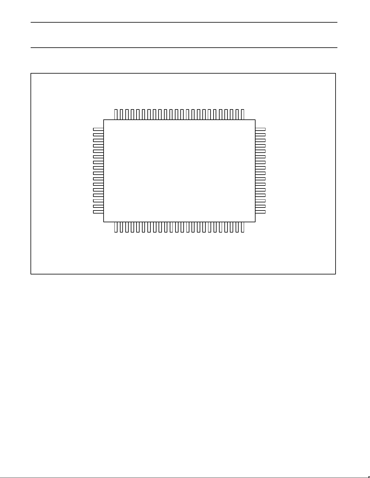
5.0 PIN CONFIGURATION
PDI1394L11
AV LINK LAYER CONTROLLER
RESERVED PHY D3
RESERVED
AV D7
RESERVED
VDD
CYCLEOUT
AV D4
PHY D7
AV D0
AV D1
AV D3
AV D2
VDD
GND
AV D5
AV D6
VDD_
GND
N/C
VDD
GND
PHY D4
PHY D5
GND
CYCLEIN
RESET_N
HIF INT _N
HIF RD_N
HIF WR_N
HIF CS_N
PHY D6
GND
AVSYNC
N/C
VDD
AVFSYNCOUT
AVFSYNCIN
AVVALID
AVCLK
SCLK
LREQ
AVENDPCK
AVERR0
N/C
GND
AVERR1
VDD
HIF D6
HIF D2
HIF D5
HIF D7
GND
VDD
HIF D4
HIF D3
HIF D0
RESERVED
HIF D1
GND
HIF A8
HIF A7
VDD
HIF A6
31
30
32
29
27
26
28
25
66
57
65
58
70
71
59
72
74
75
73
76
78
79
77
80
63
62
64
61
59
58
60
57
55
54
56
53
515052
49
2
3
1
4
6
7
5
8
10
11
9
12
141513
16
SV00270
VDD
GND
18
202119
222423
47
46
48
45
43
42
44
41
17
HIF A4
HIF A3
HIF A5
HIF A2
HIF A0
HIF A1
39
38
40
37
35
34
36
33
PHY CTL0
PHY CTL1
ISO_N
VDD
PHY D0
PHY D1
GND
PHY D2
Page 4
Philips Semiconductors Preliminary specification
PDI1394L111394 AV link layer controller
1996 Nov 06
4
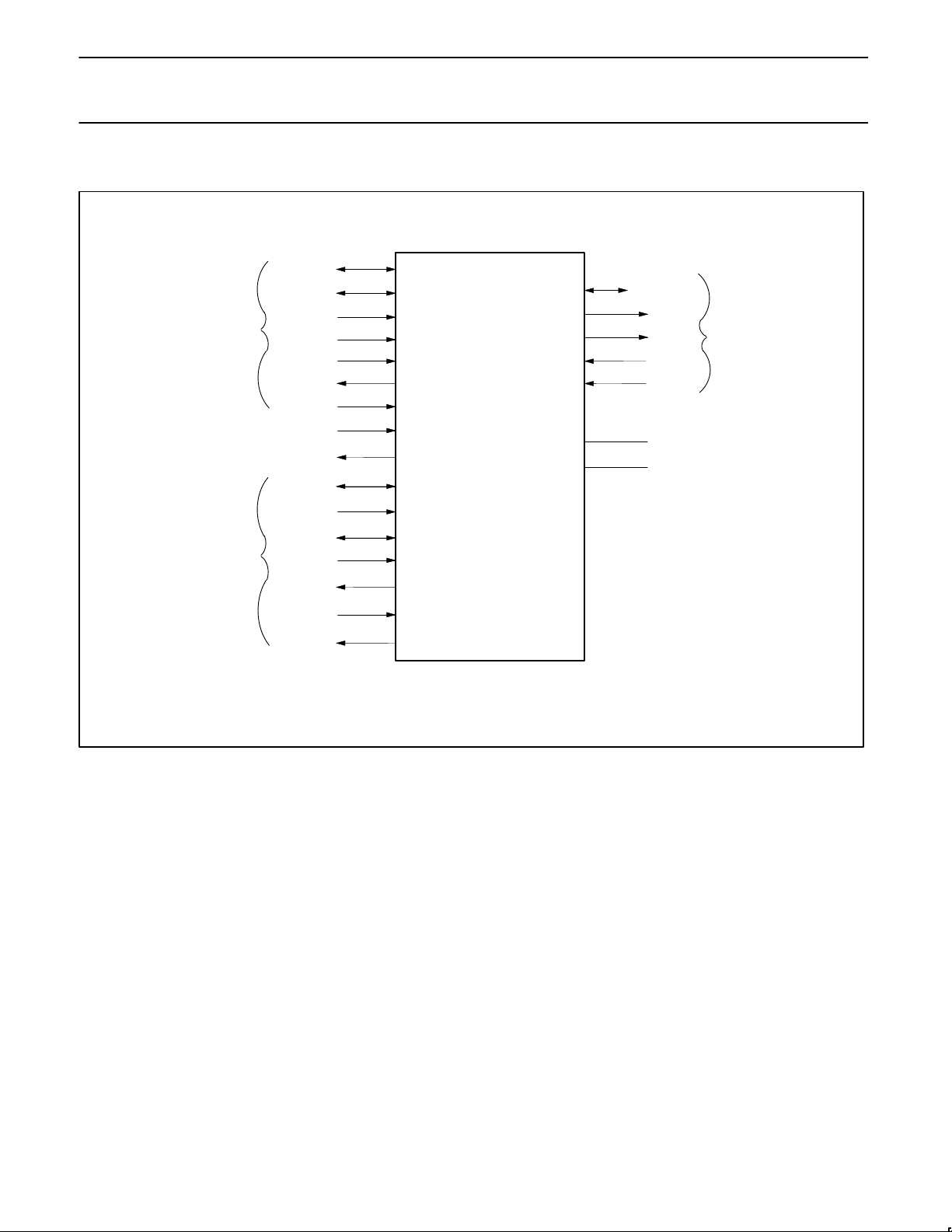
6.0 FUNCTIONAL DIAGRAM
AV LAYER
SV00267
HOST
PHY
HIF A[8:0]
HIF D[7:0]
HIF WR_N
HIF RD_N
HIF CS_N
HIF INT_N
RESET_N
CYCLEIN
CYCLEOUT
AV D[7:0]
AVCLK
AVSYNC
AFSYNCIN
AVFSYNCOUT
AVENDPCK
AVERR[1:0]
PHY D[0:7]
CTL0
LREQ
ISO_N
SCLK
VDD
GND
PDI1394L11
IEEE 1394
AV LINK LAYER CONTROLLER
Page 5
Philips Semiconductors Preliminary specification
PDI1394L111394 AV link layer controller
1996 Nov 06
5
7.0 INTERNAL BLOCK DIAGRAM
HIF A[8:0]
HIF D[7:0]
HIF WR_N
HIF RD_N
HIF CS_N
HIF INT_N
RESET_N
CYCLEIN
CYCLEOUT
AV DATA[7:0]
AVCLK
AVSYNC
AFSYNCIN
AVFSYNCOUT
AVENDPCK
AVERR1
PHY D[0:7]
CTL0
LREQ
ISO_N
SCLK
SV00269
AVERR0
AVVALID
CTL1
AV LAYER
TRANSMITTER
AND
RECEIVER
5KB
BUFFER
MEMORY
(ISOC & ASYNC
PACKETS)
LINK CORE
8-BIT
INTERFACE
ASYNC
TRANSMITTER
AND
RECEIVER
CONTROL
AND
STATUS
REGISTERS
8.0 APPLICATION DIAGRAM
SAA7201
MPEG DECODER
PDI1394L11
AV LINK
AV
INTERFACE
PDI1394P11
PHY
PHY–LINK
INTERFACE
8051
HOST CONTROLLER
DATA 8/
ADDRESS 9/
INTERRUPT & CONTROL
1394 CABLE
INTERFACE
SV00268
Page 6

Philips Semiconductors Preliminary specification
PDI1394L111394 AV link layer controller
1996 Nov 06
6
9.0 PIN DESCRIPTION
9.1 Host Interface
PIN No. PIN SYMBOL I/O NAME AND FUNCTION
14, 15, 16, 17,
18, 19, 20, 21, 22
HIF A[8:0] I
Host Interface Address 0 through 8. Provides the host with a byte wide interface to internal
registers. See description of Host Interface for addressing rules.
1, 2, 3, 4, 7, 8, 9,
10
HIF D[7:0] I/O Host Interface Data 7 (MSB) through 0. Byte wide data path to internal registers.
26 HIF WR_N I
Write enable. When asserted (LOW) in conjunction with HIF CS_N, a write to the PDI1394L1 1
internal registers is requested.
27 HIF RD_N I
Read enable. When asserted (LOW) in conjunction with HIF CS_N, a read of the PDI1394L11
internal registers is requested.
25 HIF CS_N I
Chip Select (active LOW). Host bus control signal to enable access to the FIFO and control
and status registers.
28 HIF INT_N O
Interrupt (active low). Indicates a interrupt internal to the PDI1394L11. Read the General
Interrupt Register for more information.
29 RESET_N I Reset (active low). The asynchronous master reset to the PDI1394L11.
30 CYCLEIN I
Provides the capability to supply an external cycle timer signal for the beginning of 1394 bus
cycles.
33 CYCLEOUT O Reproduces the 8kHz cycle clock of the cycle master.
6, 13, 24, 32, 39,
45, 49, 64, 72, 78
V
DD
3.0V " 0.3V power supply
5, 12, 23, 31, 38,
44, 50, 63, 73, 79
GND Ground reference
9.2 AV Interface
PIN No. PIN SYMBOL I/O NAME AND FUNCTION
77, 76, 75, 74,
71, 70, 69, 68
AVDATA[7:0] I/O Audio/Video Data 7 (MSB) through 0. Byte–wide interface to the AV layer.
58 AVCLK I External application clock. Rising edge active.
57 AVSYNC I/O Start of packet indicator.
59 AVFSYNCIN I Frame sync input, rising edge active.
60 AVFSYNCOUT O Frame sync output
56 AVENDPCK I
End of application packet indication from data source. Indicates input packet is not multiple of
DBS.
61 AVVALID I/O Indicates data on AVDATA is valid
53 AVERR0 O CRC error, indicates bus packet containing AVDATA had a CRC error.
52 AVERR1 O
Sequence Error. Indicates at least one source packet was lost before the current source
packet.
9.3 Phy Interface
PIN No. PIN SYMBOL I/O NAME AND FUNCTION
34, 35, 36, 37,
40, 41, 42, 43
PHY D[7:0] I/O
Data 0 (MSB) through 7 (NOTE: To preserve compatibility to the specified Link–Phy interface
of the IEEE 1394–1995 specification, bit 0 is the most significant bit). Data is expected on
D[0:1] for 100Mb/s, D[0:3] for 200Mb/s, and D[0:7] for 400Mb/s. See 1394 Specification for
more information.
46, 47 PHY CTL[1:0] I/O Control Lines between Link and Phy. See 1394 Specification for more information.
48 ISO_N I
Isolation barrier. This terminal is asserted (low) when an isolation barrier is present. See 1394
Specification for more information.
54 LREQ O Link Request. Bus request to access the PHY. See 1394 Specification for more information.
55 SCLK I System clock. 49.152MHz input from the PHY. Used to generate a 24.576MHz clock.
9.4 Other Pins
PIN No. PIN SYMBOL I/O NAME AND FUNCTION
65, 66, 67 RESERVED NA
These pins are reserved for factory testing. For normal operation they should be connected to
ground.
11, 51, 62, 80 N/C NA These pins are should be not be connected or terminated.
Page 7

Philips Semiconductors Preliminary specification
PDI1394L111394 AV link layer controller
1996 Nov 06
7
10.0 RECOMMENDED OPERATING CONDITIONS
LIMITS
SYMBOL
PARAMETER
CONDITIONS
UNIT
MIN.
MAX.
V
CC
DC supply voltage 3.0 3.6 V
V
I
Input voltage 0 5 V
V
IH
High-level input voltage 2.0 V
V
IL
Low-level input voltage 0.8 V
I
OH
High-level output current 8 mA
I
OL
Low-level output current –8 mA
dT/dV Input transition rise or fall time 0 20 ns/V
T
amb
Operating ambient temperature range 0 +70 °C
SCLK System clock 49.1519 49.1521 MHz
AVCLK AV interface clock
11.0 ABSOLUTE MAXIMUM RATINGS
1, 2
In accordance with the Absolute Maximum Rating System (IEC 134). Voltages are referenced to GND (ground = 0V)
LIMITS
SYMBOL
PARAMETER
CONDITIONS
MIN MAX
UNIT
V
DD
DC supply voltage –0.5 +4.6 V
I
IK
DC input diode current – –50 mA
V
I
DC input voltage –0.5 +5.5 V
I
OK
DC output diode current – " 50 mA
V
O
DC output voltage –0.5 VDD +0.5 V
I
O
DC output source or sink current – " 50 mA
I
GND
, ICCDC VCC or GND current – " 150 mA
T
stg
Storage temperature range –60 150 °C
T
amb
Operating ambient temperature 0 70 °C
P
tot
Power dissipation per package TBD W
NOTES:
1. Stresses beyond those listed may cause permanent damage to the device. These are stress ratings only and functional operation of the
device at these or any other conditions beyond those indicated under “recommended operating conditions” is not implied. Exposure to
absolute-maximum-rated conditions for extended periods may affect device reliability.
2. The performance capability of a high-performance integrated circuit in conjunction with its thermal environment can create junction
temperatures which are detrimental to reliability. The maximum junction temperature of this integrated circuit should not exceed 150°C.
11.1 Buffer Memory Sizes
BUFFER MEMORY
SIZE
(Quadlets)
Asynchronous Receive Transaction Response FIFO 64
Asynchronous Receive Transaction Request FIFO 64
Asynchronous Transmit Transaction Response FIFO 64
Asynchronous Transmit Transaction Request FIFO 64
AV Transmit/Receive Buffer 1024
Page 8

Philips Semiconductors Preliminary specification
PDI1394L111394 AV link layer controller
1996 Nov 06
8
12.0 FUNCTIONAL DESCRIPTION
12.1 Overview
The PDI1394L11 is an IEEE 1394–1995 compliant link layer controller. It provides a direct interface between a 1394 bus and various MPEG–2
and DVC codecs. Via this interface, the AV Link maps and un–maps these AV datastreams from the these codecs onto 1394 isochronous bus
packets. The AV Link also provides an 8051 / MC68XX compatible interface for an attached host controller. Through the host interface port, the
host controller can configure the AV layer for transmission or reception of AV datastreams. The host interface port also allows the host
controller to transmit and receive 1394 asynchronous data packets.
12.2 AV interface and AV layer
The AV interface and AV layer allow AV packets to be transmitted from one node to another. The AV transmitter and receiver with in the AV
layer perform all the functions required to pack and unpack AV packet data for transfer over a 1394 network. Once the AV layer is properly
configured for operation, no host controller service should be required. The host controller will have to intervene only in the case of an AV
transmit/receive buffer overrun, or other error event in the AV layer. The operation of the AV layer is half–duplex, i.e., an AV layer can either
receive or transmit AV packets at a particular time.
12.2.1 The AV Interface
The AV Link provides an 8 bit data path to the AV layer. The 8 bit data path is designed with associated clock and control signals to be
compatible with various MPEG–2 and DVC codecs.
When properly configured, the AV interface port will time stamp and buffer the incoming AV packets. The AV packet data is stored in the
embedded memory buffer, along with its time stamp information. During the next available isochronous bus cycle, the AV layer creates an
isochronous bus packet with the appropriate CIP header and AV data. The size and configuration of isochronous data packet payload
transmitted is determined by the AV layer’s configuration registers accessible through the host interface.
Once configured, the AV interface port waits for the assertion of AVVALID and AVSYNC as well as a valid AVCLK. AVSYNC is a pulse that is
aligned with the leading edge of AVCLK and the first byte of data on AVDATA[7:0]. Its duration is one AVCLK cycle. AVSYNC signals the AV
layer that the transfer of an AV packet has begun. At the time that AVSYNC is asserted, the AV layer stores the current time stamp in the buffer
memory. This time stamp is transmitted, as part of the standard packet header, to signal the receiver at what time to provide the AV packet for
output. As long as AVVALID is asserted, the data byte data present on AV DATA[7:0] at the active edge of AVCLK will be clocked into the AV
layer for processing.
At the end of the AV data packet, assertion of AVENDPCK, for one clock, will signal the AV layer that the packet is complete. This signal is
usually used when the AV packet does not fulfill the AV packet size used in the AV layer configuration.
12.2.2 IEC1883
The PDI1394L11 is specifically designed to support the proposed IEC1883 Specifications of Digital Interface for Consumer Electronic
Audio/Video Equipment. The IEC specification defines a scheme for mapping various types of AV datastreams onto 1394 isochronous data
packets. The specification also defines a software protocol for managing isochronous channels in a 1394 network called Function Control
Protocol (FCP) and Connection Management Procedures (CMP).
The mapping of AV datastreams onto 1394 isochronous packets is handled automatically by the AV Link. A special ‘AV layer’ is included in the
AV Link to manage the packing and unpacking of AV datastreams onto isochronous packets. Some features of the AV layer are automatic
time–stamping of incoming packets, buffer memory management and automatic construction of 1394 isochronous packets. Each 1394
isochronous packet generated by the AV layer contains a special header holding information specific to the packing parameters used to make
the packet. These special headers are called Common Isochronous Packet (CIP) headers.
12.2.3 CIP Headers
A feature of the IEC1883 specification is the definition of Common Isochronous Packet (CIP) headers. These CIP headers contain information
about the source and type of datastream mapped onto the isochronous packets.
The AV Layer supports the use of CIP headers. CIP headers are added to transmitted isochronous data packets at the AV data source. When
receiving isochronous data packets, the AV layer automatically analyzes their CIP headers. The analysis of the CIP headers determines the
method the AV layer uses to unpack the AV data from the isochronous data packets.
The information contained in the CIP headers is accessible via registers in the host interface.
(See proposed IEC1883 ”Specifications of Digital Interface for Consumer Electronic Audio/Video Equipment” December 1995, Section 6 for
more details on CIP headers).
Page 9

Philips Semiconductors Preliminary specification
PDI1394L111394 AV link layer controller
1996 Nov 06
9
12.3 Host interface Port
The PDI1394L11 Host interface provides an 8 bit (bytewide) data path, 9 address lines, and associated control lines to access the AV Link
Controller’s 32–bit internal registers. The interfacing scheme allows the bytewide data path to access the internal registers in 4 accesses.
12.3.1 Using the Host Interface
The PDI1394L11 Host interface provides an 8 bit (bytewide) data path, 9 address lines, and assorted control lines to access the AV Link
Controller’s 32–bit internal registers. The interfacing scheme allows the bytewide data path to access the internal registers in 4 accesses.
12.3.2 Addressing Scheme
The PDI1394L11 contains twenty–nine (29) 32–bit internal registers. These registers are accessible through the 8–bit host interface data path
using a quadlet–to–byte multiplexing scheme. The multiplexing scheme involves reading or writing the contents of an internal register to a
shadow register. The shadow register provides the host interface with access to the internal register’s contents, one byte at a Tinsmith. The
host interface contains a 32–bit shadow register that is used to temporarily store internal register data during reads or writes. Host interface
Address bit 8 (HIF ADDR8) is used to signal internal logic to either transfer the contents of an internal 32–bit register to the host interface
shadow register, in the case of a read, or transfer the contents of the host interface shadow register to an internal 32–bit register, in the case of
a write. Reading the shadow register with HIF A8=1 is called a read with update, writing to the shadow register with HIF A8=1 is called a write
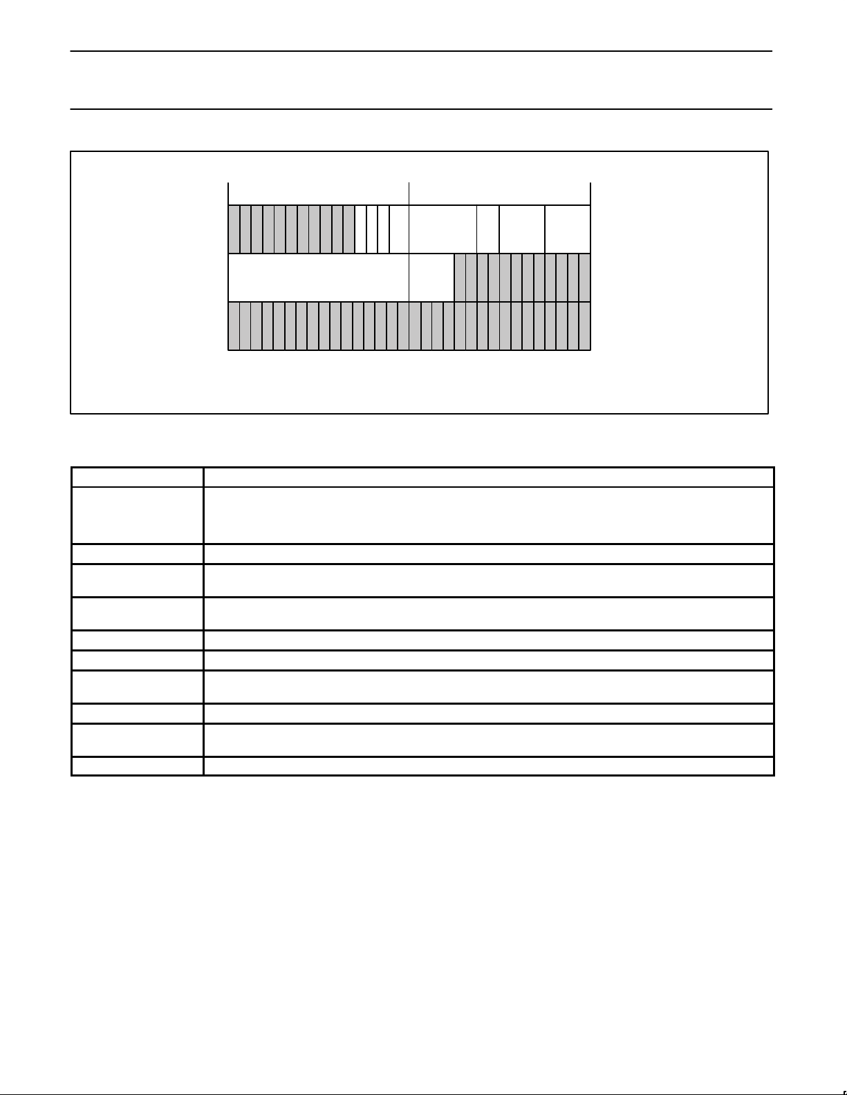
with update. Successive reads to the other 3 bytes of the 32–bit register should not have HIF A8 set. An example of accessing the General
Control Register is shown in Figure 1.
The host interface uses 9 address bits to form the bytewide addresses. Each internal 32–bit register has a base address that points to the
lowest order byte in the register. The next three addresses (base address+1, +2, and +3) are the next higher order bytes of the 32–bit internal
register. Note that base address+0 retrieves or writes the most significant byte, bits 31–24, of a 32–bit register; base address+1 retrieves or
writes the next most significant byte, bits 23–16 of a 32–bit register; and so on.
**********************
This code segment shows how to read the General Control Register, located at address 0x004 and move its contents to an array
located at TEMP.
**********************
MOVE 0x104, TEMP Gets contents of GENCTL bits 31–24, low byte, and moves it to TEMP
MOVE 0x005, TEMP+1 Gets the next byte of GENCTL bits 23–16 and moves it to TEMP+1
MOVE 0x006, TEMP+2 Gets the 3rd byte of GENCTL bits 15–8 and moves it to TEMP+2
MOVE 0x007, TEMP+3 Gets the last byte of GENCTL bits 7–0 and moves it to TEMP+3
**********************
This code segment shows how to write the General Control Register, located at address 0x004 with the contents of an array
located at TEMP.
**********************
MOVE TEMP, 0x004 Moves TEMP to the first byte of GENCTL, bits 31–24
MOVE TEMP+1,0x005 Moves TEMP+1 to the second byte of GENCTL, bits 23–16
MOVE TEMP+2, 0x006 Moves TEMP+2 to the 3rd byte of GENCTL, bits 15–8
MOVE TEMP+3, 0x107 Moves TEMP+3 to the last byte of GENCTL, bits 7–0, and performs the write with update
SV00266
Figure 1. General Control Register Read/Write Code Segments
Page 10
Philips Semiconductors Preliminary specification
PDI1394L111394 AV link layer controller
1996 Nov 06
10
12.4 The Asynchronous Packet Interface
The PDI1394L11 provides an interface to asynchronous data packets through the registers in the host interface. The format of the
asynchronous packets is specified in the following sections.
12.4.1 Reading an Asynchronous Packet
Upon reception of a packet, the packet data is stored in the appropriate receive FIFO, either the Request or Response FIFO. The location of
the packet is indicated by either the RXRQA or RXRPA status bit being set in the Asynchronous RX/TX Control 2 (ASY_CR2) register. The
packet is transferred out of the FIFO by successive reads of the Asynchronous Receive Request (RX_RQ) or Asynchronous Receive Response
(RX_RP) register. The end of the packet (the last quadlet) is indicated by either the RXRPL or RXRQL bit set in ASY_CR2. Continuing to try to
read the FIFO after the last quadlet has been read will result in a queue read error indicated by the either RXRQE bit or RXRPE bit being set in
Asynchronous RX/TX Control 2 (ASY_CR2) register.
12.4.2 Writing an Asynchronous Packet
An asynchronous packet intended for transmission is first stored in the appropriate Transmitter FIFO. Once writing to the FIFO is complete, the
link layer controller arbitrates for the bus to transmit the packet.
To generate an asynchronous packet, the first and next to last quadlets of the packet must be written to the Asynchronous Transmit Request
Nextone (TX_RQ_NEXT) register, for request type packets, or the Asynchronous Transmit Response Next (TX_RP_NEXT) register, for
response type packets. The last quadlet of the packet is written to the Asynchronous Transmit Request Last (TX_RQ_LAST) register, for
request type packets, or the Asynchronous Transmit Response Last (TX_RP_LAST) register, for response type packets. After writing the last
quadlet, the packet is automatically queued by the AVlink layer controller for transmission over the bus.
12.5 Link Packet Data Formats
The data formats for transmission and reception of data are shown below. The transmit format describes the expected organization for data
presented to the link at the asynchronous transmit, physical response, or isochronous transmit FIFO interfaces. The receive format of data link
presents at the receive FIFO interface.
12.5.1 Asynchronous Transmit
There are four basic formats for asynchronous data to be transmitted:
1. no–data packets (used for quadlet read requests and all write responses)
2. quadlet packets (used for quadlet write requests, quadlet read responses, and block read requests)
3. block packets (used for lock requests and responses, block write requests, and block read responses)
4. unformatted data.
12.5.1.1 No–data Transmit
The no–data transmit format is shown in Table 1. The first quadlet contains packet control information. The second and third quadlets contain
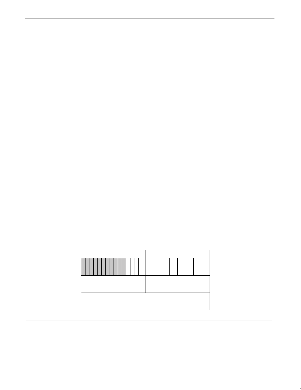
16–bit destination ID and either the 48–bit, quadlet aligned destination offset(for requests) or the response code (for responses).
destinationID
spd tLabel rt
tCode priority
imm
enable AT
31
30
29 28 27 2625
24 23 22 212019 18 1716
15 141312
1110 987 6 5 4 3 2 1 0
destinationOffsetHigh
SV00250
destinationOffsetLow
Figure 2. Quadlet Read Request Tansmit Format
Page 11
Philips Semiconductors Preliminary specification
PDI1394L111394 AV link layer controller
1996 Nov 06
11
destinationID
spd tLabel rt
tCode priority
imm
enable AT
SV00249
31
30
29 28 27 2625
24 23 22 212019 18 1716
15 141312
1110 987 6 5 4 3 2 1 0
rCode
Figure 3. Write Response Transmit Format
Table 1. No-Data Transmit Format
Field Name Description
enableAT Re–enable asynchronous transmit operation. After a bus reset, all asynchronous transmit packets are flushed until
a packet header with this bit is set is presented. Important: this bit should only be set for a single packet after a bus
reset is detected. Normally this bit should be cleared, allowing the link core to flush queued packets that may no
longer be correctly addressed after a bus reset.
imm Always set to $0’.
spd This field indicates the speed at which this packet is to be sent. 00=100 Mbs, 01=200 Mbs, and 10=400 Mbs.
11 = undefined
tLABEL This field is the transaction label, which is used to pair up a response packet with its corresponding request
packet.
rt The retry code for this packet. 00=retry 1, 01=retryX, 10=retryA, 11=retryB
tCode The transaction code for this packet.
Priority The priority level for this packet. Any non–zero value directs the transmitter to use priority arbitration for this
packet.
DestinationID This is the concatenation of the 10–bit bus address and the 6–bit node number for the destination of this packet.
DestinationOffsetHigh
DestinationOffsetLow
The concatenation of these two field addresses a quadlet in the destination node’s address space. This address
must be quadlet–aligned (modulo 4).
RCode Response code for write response packet.
Page 12
Philips Semiconductors Preliminary specification
PDI1394L111394 AV link layer controller
1996 Nov 06
12
12.5.1.2 Quadlet Transmit
Three quadlet transmit formats are shown below. In these figures: The first quadlet contains packet control information. The second and third
quadlets contain 16–bit destination ID and either the 48–bit quadlet–aligned destination offset (for requests) or the response code (for
responses).
The fourth quadlet contains the quadlet data for read response and write quadlet request formats, or the upper 16 bits contain the data length
for the block read request format.
destinationID
spd tLabel rt
tCode priority
imm
enable AT
31
30
29 28 27 2625
24 23 22 212019 18 1716
15 141312
1110 987 6 5 4 3 2 1 0
destinationOffsetHigh
destinationOffsetLow
quadlet data
SV00251
Figure 4. Quadlet Write Request Transmit Format
destinationID
spd tLabel rt
tCode priority
imm
enable AT
31
30
29 28 27 2625
24 23 22 212019 18 1716
15 141312
1110 987 6 5 4 3 2 1 0
rCode
quadlet data
SV00252
Figure 5. Quadlet Read Request Transmit Format
Page 13
Philips Semiconductors Preliminary specification
PDI1394L111394 AV link layer controller
1996 Nov 06
13
destinationID
spd tLabel rt
tCode priority
imm
enable AT
31
30
29 28 27 2625
24 23 22 212019 18 1716
15 141312
1110 987 6 5 4 3 2 1 0
destinationOffsetHigh
destinationOffsetLow
data length
SV00253
Figure 6. Block Read Request Transmit Format
Table 2. Quadlet Transmit Fields
Field Name Description
enableAT, imm, spd, tLabel, rt, tCode, priority, destinationID,
destinationOffsetHigh, destinationOffsetLow, rCode
See Table 1
Quadlet data For quadlets write requests and quadlet read responses, this field
holds the data to be transferred
Data length The number of bytes requested in a block read request
12.5.1.3 Block Transmit
The block transmit format is shown below, this is the generic format for reads and writes. The first quadlet contains packet control information.
The second and third quadlets contain the 16–bit destination node ID and either the 48–bit destination offset (for requests) or the response code
and reserved data (for responses). The fourth quadlet contains the length of the data field and the extended transaction code (all zeros except
for lock transaction). The block data, if any, follows the extended code.
destinationID
spd tLabel rt
tCode priority
imm
enable AT
31
30
29 28 27 2625
24 23 22 212019 18 1716
15 141312
1110 987 6 5 4 3 2 1 0
destinationOffsetHigh
destinationOffsetLow
dataLength extendedTcode
Block Length
padding (if needed)
SV00254
Figure 7. Block Transmit Format
Page 14
Philips Semiconductors Preliminary specification
PDI1394L111394 AV link layer controller
1996 Nov 06
14
spd tLabel rt
tCode priority
imm
enable AT
31
30
29 28 27 2625
24 23 22 212019 18 1716
15 141312
1110 987 6 5 4 3 2 1 0
dataLength extendedTcode
Block Length
padding (if needed)
SV00255
destinationID
rCode
Figure 8. Block Read or Lock Response Transmit Format
Table 3. Block Transmit Field
Field Name Description
enableAT, imm, spd, tLabel, rt, tCode, priority, destinationID,
destinationOffsetHigh, destinationOffsetLow, rCode
See Table 2.
dataLength The number of bytes of data to be transmitted in this packet
extendedTcode The tCode indicates a lock transaction, this specifies the actual lock
action to be performed with the data in this packet.
block data The data to be sent. If dataLength=0, no data should be written into
the FIFO for this field. Regardless of the destination or source
alignment of the data, the first byte of the block must appear in the
high order byte of the first quadlet.
padding If the dataLength mod 4 is not zero, then zero–value bytes are added
onto the end of the packet to guarantee that a whole number of
quadlets is sent.
Page 15

Philips Semiconductors Preliminary specification
PDI1394L111394 AV link layer controller
1996 Nov 06
15
12.5.1.4 Unformatted Transmit
The unformatted transmit format is shown in Figure 9. The first quadlet contains packet control information. The remaining quadlets contain data
that is transmitted without any formatting on the bus. No CRC is appended on the packet, nor is any data in the first quadlet sent. This is used to
send PHY configuration and Link–on packets. Note that the bit–inverted check quadlet must be included in the FIFO since the AV Link core will
not generate it.
spd tLabel
tCode priority
enable AT
31
30
29 28 27 2625
24 23 22 212019 18 1716
15 141312
1110 987 6 5 4 3 2 1 0
unformatted packet data
SV00256
Figure 9. Unformatted Transmit Format
12.5.2 Asynchronous Receive
There are four basic formats for asynchronous data to be received:
1. no–data packets (used for quadlet read requests and all write responses)
2. quadlet packets (used for quadlet write requests, quadlet read responses, and block read requests),
3. block packets (used for lock requests and responses, block write requests, and block read responses),
4. self–ID data. The names and descriptions of the fields in the received data are given in Table 4.
Page 16

Philips Semiconductors Preliminary specification
PDI1394L111394 AV link layer controller
1996 Nov 06
16
Table 4. Asynchronous Receive Fields
Field Name Description
destinationID This field is the concatenation of busNumbers (or all ones for “local bus” and nodeNumbers or all ones for
broadcast) for this node.
tLabel This field is the transaction label, which is used to pair up a response packet with its corresponding request
packet.
rt The retry code for this packet. 00=retry1, 01=retryX, 10=retryA, 11=retryB.
tCode The transaction code for this packet. In this case 0xE (HEX, E)
priority The priority level for this packet.
sourceID This is the node ID of the sender of this packet.
destinationOffsetHigh,
destinationOffsetLow
The concatenation of these two field addresses a quadlet in this node’s address space. This address must be
quadlet–aligned (modulo 4).
rCode Response code for response packets.
quadlet data For quadlet write requests and quadlet read responses, this field holds the data received.
dataLength The number of bytes of data to be received in a block packet.
extendedTcode If the tCode indicates a lock transaction, this specifies the actual lock action to be performed with the data in
this packet.
block data The data received. If dataLength=0, no data will be written into the FIFO for this field. Regardless of the
destination or source alignment of the data, the first byte of the block will appear in the high order byte of the
first quadlet.
padding If the dataLength mod 4 is not zero, then zero–value bytes are added onto the end of the packet to guarantee
that a whole number of quadlets is sent.
12.5.2.1 No–Data Receive
The no–data receive formats are shown below. The first quadlet contains the destination node ID and the rest of the packet header. The second
and third quadlet contain 16–bit source ID and either the 48–bit, quadlet–aligned destination offset (for requests) or the response code (for
responses). The last quadlet contains packet reception status.
destinationID
tLabel rt
tCode priority
31
30
29 28 27 2625
24 23 22 212019 18 1716
15 141312
1110 987 6 5 4 3 2 1 0
destinationOffsetHigh
destinationOffsetLow
sourceID
SV00257
spd
ackSent
Figure 10. Quadlet Read Request Receive Format
Page 17

Philips Semiconductors Preliminary specification
PDI1394L111394 AV link layer controller
1996 Nov 06
17
destinationID
tLabel rt
tCode priority
31
30
29 28 27 2625
24 23 22 212019 18 1716
15 141312
1110 987 6 5 4 3 2 1 0
rCode
sourceID
SV00258
spd
ackSent
Figure 11. Write Response Receive Format
12.5.2.2 Quadlet Receive
The quadlet receive formats are shown below. The first quadlet contains the destination node ID and the rest of the packet header. The second
and third quadlets contain 16–bit source ID and either the 48–bit, quadlet–aligned destination offset (for requests) or the response code (for
responses). The fourth quadlet is the quadlet data for read responses and write quadlet requests, and is the data length and reserved for block
read requests. The last quadlet contains packet reception status.
destinationID
tLabel rt
tCode priority
31
30
29 28 27 2625
24 23 22 212019 18 1716
15 141312
1110 987 6 5 4 3 2 1 0
destinationOffsetHigh
destinationOffsetLow
sourceID
quadlet data
SV00259
spd
ackSent
Figure 12. Quadlet Read Request Receive Format
Page 18

Philips Semiconductors Preliminary specification
PDI1394L111394 AV link layer controller
1996 Nov 06
18
destinationID
tLabel rt
tCode priority
31
30
29 28 27 2625
24 23 22 212019 18 1716
15 141312
1110 987 6 5 4 3 2 1 0
rCode
sourceID
quadlet data
SV00260
spd
ackSent
Figure 13. Quadlet Read Response Receive Format
destinationID
tLabel rt
tCode priority
31
30
29 28 27 2625
24 23 22 212019 18 1716
15 141312
1110 987 6 5 4 3 2 1 0
destinationOffsetHigh
destinationOffsetLow
sourceID
data length
SV00261
spd
ackSent
Figure 14. Block Read Request Receive Format
Page 19

Philips Semiconductors Preliminary specification
PDI1394L111394 AV link layer controller
1996 Nov 06
19
12.5.2.3 Block receive
The block receive format is shown below. The first quadlet contains the destination node ID and the rest of the packet header. The second and
third quadlets contain 16–bit sourceID and either the 48–bit destination offset (for requests) or the response code and reserved data (for
responses). The fourth quadlet contains the length of the data field and the extended transaction code (all zeros except for lock transactions).
The block data, if any, follows the extended code. The last quadlet contains packet reception status.
dataLength extendedTcode
Block Length
padding (if needed)
destinationID
tLabel rt
tCode priority
31
30
29 28 27 2625
24 23 22 212019 18 1716
15 141312
1110 987 6 5 4 3 2 1 0
destinationOffsetHigh
destinationOffsetLow
sourceID
SV00262
spd
ackSent
Figure 15. Block Write or Lock Request Receive Format
Page 20

Philips Semiconductors Preliminary specification
PDI1394L111394 AV link layer controller
1996 Nov 06
20
destinationID
tLabel rt
tCode priority
31
30
29 28 27 2625
24 23 22 212019 18 1716
15 141312
1110 987 6 5 4 3 2 1 0
rCode
sourceID
dataLength extendedTcode
Block Length
padding (if needed)
SV00263
spd
ackSent
Figure 16. Block Read or Lock Response Receive Format
12.5.2.4 Self–ID and PHY packets receive
The self–ID and PHY packet receive formats are shown below. The first quadlet contains a synthesized packet header with a tCode of 0x0E
(hex). For self–IDinformation, the remaining quadlets contain data that is received from the time a bus reset ends to the first subaction gap. This
is the concatenation of all the self–ID packets received. Note that the bit–inverted check quadlet is included in the FIFO and the application must
check it.
31
30
29 28 27 2625
24 23 22 212019 18 1716
15 141312
1110 987 6 5 4 3 2 1 0
self ID packet data
1110
2
0000
2
SV00264
00
ackSent
Figure 17. Self-ID Receive Format
The “ackSent” field will either be “ACK_DATA_ERROR” if a non–quadlet–aligned packet is received or there was a data overrun, or
“ACK_COMPLETE” if the entire string of self–ID packets was received.
Page 21

Philips Semiconductors Preliminary specification
PDI1394L111394 AV link layer controller
1996 Nov 06
21
31
30
29 28 27 2625
24 23 22 212019 18 1716
15 141312
1110 987 6 5 4 3 2 1 0
PHY packet first quadlet
1110
2
0000
2
SV00265
Figure 18. PHY Packet Receive Format
For PHY packets, there is a single following quadlet which is the first quadlet of the PHY packet. The check quadlet has already been verified
and is not included.
12.5.3 Interrupts
The PDI1394L11 provides a single interrupt line (HIF INT_N) for connection to a host controller. Status indications from four major areas of the
device are collected and ORed together to activate HIF INT_N. Status from four major areas of the device are collected in four status registers;
LKPYINTA, ITXINTA, IRXINTA, and ASY_CR2. At this level, each individual status can be enabled to generate a chip–level interrupt by
activating HIF INT_N. To aid in determining the source of a chip–level interrupt, the major area of the device generating an interrupt is indicated
in the lower 4 bits of the GENINT register. These bits are non–latching status bits and do not need to be acknowledged. To acknowledge and
clear a standing interrupt, the bit in LKPYINTA, ITXINTA, IRXINTA, or ASY_CR2 causing the interrupt status has to be acknowledged.
12.5.3.1 Determining and Clearing Interrupts
When responding to an interrupt event generated by the PDI1394L11, or operating in polled mode, the first register examined is the GENINT
register. The least significant nibble contains interrupt status bits from general sections of the device; the link layer controller, the AV transmitter,
the AV receiver, and the asynchronous transceiver. The bits in GENINT[3:0] are self clearing status bits. They represent the logical OR of all
the enabled interrupt status bits in their section of the AV Link Layer Controller.
Once an interrupt, or status is detected in GENINT, the appropriate interrupt status register needs to be read, see the Interrupt Hierarchy
diagram for more detail. After all the interrupt indications are dealt with in the appropriate interrupt status register, the interrupt status indication
will automatically clear in the GENINT.
All interrupt status bits in the various interrupt status registers are latching unless otherwise noted.
Page 22

Philips Semiconductors Preliminary specification
PDI1394L111394 AV link layer controller
1996 Nov 06
22
12.5.3.2 Interrupt Hierarchy
18 17 16
15 141312
1110 987 6 5 4 3 2 1 0
SV00271
22 21 20
19 18
17 16
141312
1110 987 6 5 4 3 2 1 0
7 6 5 4 3 2 1 0
3 2 1 0
ITxINTCTL (0x02C
IRxINTCTL (0x04C)
ASY_CR2 (0x084)
LKPYINTA (0x008)
GENINT (0x004)
HIF INT_N
PHYINT
CMDRST
FAIRGAP
PHYRRX
ITSTUCK
PHYRST
TxRDY
ATSTUCK
STNREJ
HDRERR
ARBGAP
RxDATA
CYST
TCERR
CYTMOUT
CYDNE
CYPND
CYLST
CYSEC
RxRPE
SID
RxRPF
RxRQE
RxRPA
RxRQA
RxRQF
RPCFA
IDDSCI
SYTTI
EOTI
PLDSCI
ITxMFI
ITxMEI
DBCEI
SEQEI
IRxMFI
IRxMEI
CRCEI
TAGEI
RxBPI
FSYI
SQOVI
TxRPF
TxRQF
TxRPE
TxRQE
RQCFA
TxRPI
TxRQI
Page 23

Philips Semiconductors Preliminary specification
PDI1394L111394 AV link layer controller
1996 Nov 06
23
13.0 REGISTER MAP
13.1 Link Control Registers
13.1.1 ID Register (ID) – Base Address: 0x000
The ID register is automatically updated by the attached PHY with the proper Node ID after completion of the bus reset.
31
30
29 28 27 2625
24 23 22 212019 18 1716
15 141312
1110 987 6 5 4 3 2 1 0
SV00272
NODE ID
BUS ID VERSION CODE
Reset Value 0xFFFF0001
Bit 31..22: R/W Bus ID:The 10–bit bus number that is used with the Node ID in the source address for outgoing packets and used to
accept or reject incoming packets.
Bit 21..16: R/W Node ID: Used in conjunction with Bus ID in the source address for outgoing packets and used to accept or reject
incoming packets. This register auto–updates with the node ID assigned after the 1394 bus Tree–ID sequence.
Bit 15..0: R Version Code: Version of the PDI1394L11
13.1.2 General Link Control (GENCTL) – Base Address: 0x004
The General Link control register is used to program the Link Layer isochronous transceiver, as well as the overall link transceiver. It also
provides general link status.
31
30
29 28 27 2625
24 23 22 212019 18 1716
15 141312
1110 987 6 5 4 3 2 1 0
SV00273
IDVALID
RCVSELFID
ROOT
BSYFLAG
CYTMREN
STICT ISOC
CYMASTER
CYSOURCE
RST Tx
RST Rx
TxENABLE
RxENABLE
BSYCTRL
ATACK
Reset Value 0x40300000
Bit 31: R/W ID Valid: When equal to one, the PDI1394L11 accepts the packets addressed to this node.
Bit 30: R/W Receive Self ID: When asserted, the self–identification packets, generated by each PHY device on the bus, during
bus initialization are received and placed into the asynchronous request queue as a single packet.
Bit 29..27: R/W Busy Control: These bits control what busy status the chip returns to incoming packets. The field is defined below:
000 = follow normal busy/retry protocol, only send busy when necessary
001 = send busy A when it is necessary to send a busy acknowledge
010 = send a busy B when it is necessary to send a busy acknowledge
011 = reserved
100 = send a busy acknowledge to all incoming packets following the normal busy/retry protocol
101 = send a busy acknowledge to all incoming packets by sending a busyA acknowledge
111 = reserved
Bit 26: R/W Transmitter Enable: When this bit is set, the link layer transmitter will arbitrate and send packets.
Bit 25: R/W Receiver Enable: When this bit is set, the link layer receiver will receive and respond to bus packets.
Page 24

Philips Semiconductors Preliminary specification
PDI1394L111394 AV link layer controller
1996 Nov 06
24
Bit 21: R/W Reset Transmitter: When set to one, this synchronously resets the transmitter within the link layer.
Bit 20: R/W Reset Receiver: When set to one, this synchronously resets the receiver within the link layer.
Bit 12: R/W Strict Isochronous: Used to accept or reject packets sent outside of specified isochronous cycles (between a Cycle
Start and subaction gap). A “1” rejects packets sent outside the specified cycles, a “0” accepts isochronous packets
sent outside the specified cycle. For standard operation, this bit should be set.
Bit 11: R/W Cycle Master: When asserted the PDI1394L11 is attached to the root PHY (ROOT bit = 1). When the cycle_count
field of the cycle timer register increments, the transmitter sends a cycle–start packet.
Bit 10: R/W Cycle Source: When asserted, the cycle_count field increments and the cycle_offset field resets for each positive
transition of CYCLEIN. When deasserted, the cycle count field increments when the cycle_offset field rolls over.
Bit 9: R/W Cycle Timer Enable: When asserted, the cycle offset field increments.
Bit 5: R Root: Indicates this device is the root on the bus.
Bit 4: R Busy Flag: The type of busy acknowledge which will be sent next time an acknowledge is required. 0 = Busy A, 1 =
Busy B (only meaningful during a dual–phase busy/retry operation).
Bit 3..0: R AT acknowledge received: The last acknowledge received by the transmitter in response to a packet sent from the
transmit–FIFO interface while the ATF is selected.
13.1.3 Link /Phy Interrupt Acknowledge (LKPYINTA) – Base Address: 0x008
The Link/Phy Interrupt Acknowledge register indicates various status and error conditions in the Link and Phy which can be programmed to
generate an interrupt. The interrupt enable register (LKPYINTE) is a mirror of this register. Acknowledgment of an interrupt is accomplished by
writing a ‘1’ to a bit in this register that is set. This action reset the bit indication to a ‘0’.
31
30
29 28 27 2625
24 23 22 212019 18 1716
15 141312
1110 987 6 5 4 3 2 1 0
SV00274
CMDRST
FAIRGAP
HDRERR
TCERR
ARBGAP
PHYINT
STNREJ
RxDATA
ITSTUCK
ATSTUCK
PHYRRX
TxRDY
CYTMOUT
PHYRST
CYDNE
CYPND
CYST
CYSEC
CYLST
Reset Value 0x00000000
Bit 18: R/W Command Reset Received: The receiver has confirmed data to the GRF interface.
Bit 17: R/W Fair Gap: The serial bus has been idle for a fair–gap time.
Bit 16: R/W Arbitration Reset Gap: The serial bus has been idle for an arbitration reset gap.
Bit 15: R/W Phy Chip Int: The Phy chip has signaled an interrupt through the Phy interface.
Bit 14: R/W Phy Register Information Received: A register has been transferred to the Phy chip input register.
Bit 13: R/W Phy Reset Started: A Phy–layer reconfiguration has started. This interrupt clears the ID valid bit.
Bit 12: R/W Transmitter Ready: The transmitter is idle and ready.
Bit 11: R/W Receiver has Data: The receiver has confirmed data to the GRF interface.
Bit 10: R/W Isochronous Transmitter is Stuck: The transmitter has detected invalid data at the transmit–FIFO interface when the
ITF is selected.
Bit 9: R/W Asynchronous Transmitter is Stuck: The transmitter has detected invalid data at the transmit–FIFO interface when
the ATF is selected.
Bit 8: R/W Busy Acknowledge Sent by Receiver: The receiver is forced to send a busy acknowledge to a packet addressed to
this node because the GRF overflowed.
Bit 7: R/W Header Error: The receiver detected a header CRC error on an incoming packet that may have been addressed to
this node.
Bit 6: R/W Transaction Code Error: The transmitter detected an invalid transaction code in the data at the transmit FIFO
interface.
Bit 5: R/W Cycle Timed Out.
Bit 4: R/W Cycle Second incremented: The cycle second field in the cycle–timer register incremented. this occurs
approximately every second when the cycle timer is enabled.
Bit 3: R/W Cycle Started: The transmitter has sent or the receiver has received a cycle start packet.
Page 25

Philips Semiconductors Preliminary specification
PDI1394L111394 AV link layer controller
1996 Nov 06
25
Bit 2: R/W Cycle Done: A fair gap has been detected on the bus after the transmission or reception of a cycle start packet. This
indicated that the isochronous cycle is over.
Bit 1: R/W Cycle Pending: Cycle pending is asserted when cycle timer offset is set to zero (rolled over or reset) and stays
asserted until the isochronous cycle has ended.
Bit 0: R/W Cycle Lost: The cycle timer has rolled over twice without the reception of a cycle start packet. This only occurs when
cycle master is not asserted.
13.1.4 Link / Phy Interrupt Enable (LKPYINTE) – Base Address: 0x00C
This register is a mirror of the Link/Phy Interrupt Acknowledge (LKPYINTA) register. Enabling an interrupt is accomplished by writing a ‘1’ to the
bit corresponding to the interrupt desired.
31
30
29 28 27 2625
24 23 22 212019 18 1716
15 141312
1110 987 6 5 4 3 2 1 0
CMDRST
FAIRGAP
HDRERR
TCERR
ARBGAP
PHYINT
STNREJ
RxDATA
ITSTUCK
ATSTUCK
PHYRRX
TxRDY
CYTMOUT
PHYRST
CYDNE
CYPND
CYST
CYSEC
CYLST
SV00275
This register enables the interrupts described in the Link /Phy Interrupt Acknowledge register description. A one in any of the bits enables that
function to create an interrupt. A zero disables the interrupt, however the status is readable in the Link /Phy Interrupt Acknowledge register.
Reset Value 0x00000000
13.1.5 Cycle Timer Register (CYCTM) – Base Address: 0x010
Cycle Timer Register operation is controlled by the Cycle Timer Enable (CYTMREN) bit in the General Control Register.
31
30
29 28 27 2625
24 23 22 212019 18 1716
15 141312
1110 987 6 5 4 3 2 1 0
CYCLE SECONDS CYCLE NUMBER
CYCLE OFFSET
SV00276
Reset Value 0x00000000
Bit 31..25: R/W Seconds count: 1–Hz cycle timer counter.
Bit 24..12: R/W Cycle Number: 8kHz cycle timer counter.
Bit 11..0: R/W Cycle Offset: 24.576MHz cycle timer counter.
13.1.6 Phy Register Access (PHYACS) – Base Address: 0x014
This register provides access to the internal registers on the Phy. There are special considerations when reading or writing to this register.
When reading a PHY register, the address of the register is written to the Phy Rg Ad field with the Rd Phy bit set. The register is then read
again until Rd Phy clears. Once this happens the register data is available in the Phy Rx Data, the address of the register just read is also
Page 26

Philips Semiconductors Preliminary specification
PDI1394L111394 AV link layer controller
1996 Nov 06
26
available in the Phy Rx Ad fields. When writing a Phy register, the address of the register to be written is set in the Phy Rg Ad field and the data
to be written to the register is set in Phy Rg Data, along with the WrPhy bit being set. Once the write is complete, the WrPhy bit will be cleared.
31
30
29 28 27 2625
24 23 22 212019 18 1716
15 141312
1110 987 6 5 4 3 2 1 0
RDPHY
WRPHY
SV00277
PHYRGAD
PHYRGDATA PHYRXAD PHYRXDATA
Reset Value 0x00000000
Bit 31: R/W Read Phy Chip Register: When asserted, the PDI1394L1 1 sends a read register request with address equal to Phy
Rg Ad to the Phy interface. This bit is cleared when the request is sent.
Bit 30: R/W Write Phy Chip Register: When asserted, the PDI1394L11 sends a write register request with address equal to Phy
Rg Ad to the Phy interface. This bit is cleared when the request is sent.
Bit 27..24: R/W Phy Chip Register Address: This is the address of the Phy–chip register that is to be accessed.
Bit 23..16: R/W Phy Chip Register Data: This is the data to be written to the Phy–chip register indicated in Phy Rg Ad.
Bit 11..8: R Phy Chip Register Received Address: Address of register from which Phy Rx Data came.
Bit 7..0: R Phy Chip Register Received Data: Data from register addressed by Phy Rx Ad.
13.1.7 General Interrupt Status and TX Control (GENINT) – Base Address: 0x018
This register is the top level interrupt status register. If the external interrupt line is set, this register will indicate which major portion of the AV
Link generated the interrupt. There is no interrupt acknowledge required at this level. These bits auto clear when the interrupts in the
appropriate section of the device clears all its interrupt statuses, or they are disabled. Control of the AV transceiver is also provided by this
register.
31
30
29 28 27 2625
24 23 22 212019 18 1716
15 141312
1110 987 6 5 4 3 2 1 0
SV00278
TXMODE
ASYTX/RX
AVTXINT
AVRXINT
LKPHYINT
Bits 0 through 4 are used to identify to source of a general interrupt. When identified, the appropriate register needs to be read to find the exact
source of the interrupt.
Reset Value 0x00010000
Bit 16: R/W Transmit Mode: Control bit, a “1” enables the AV transmitter. A “0” enables the AV receiver. The register defaults to
“1” on reset.
Bit 3: R Asynchronous Transmitter/ Receiver Interrupt: Interrupt source is in the Asynchronous Transmitter/ Receiver
Interrupt Acknowledge/Source register.
Bit 2: R AV Transmitter Interrupt: Interrupt source is in the AV Transmitter Interrupt Acknowledge/Source register .
Bit 1: R AV Receiver Interrupt: Interrupt source is in the AV Receiver Interrupt Acknowledge/Source register.
Bit 0: R Link–Phy Interrupt: Interrupt source is in the Link Phy Interrupt Acknowledge register.
Page 27

Philips Semiconductors Preliminary specification
PDI1394L111394 AV link layer controller
1996 Nov 06
27
13.2 AV Transmitter and Receiver Registers
13.2.1 AV Transmit Packing Control and Status (ITXCTL) – Base Address: 0x020
31
30
29 28 27 2625
24 23 22 212019 18 1716
15 141312
1110 987 6 5 4 3 2 1 0
EN_ITX
EN_FS
RST_ITX
SV00279
PMTRDEL MAXBL
Reset Value 0x00000001
Bit 27..16: R/W TRDEL: Transport delay. Value added to time stamp before transmission takes place. Lower 4 bits add to upper
4 bits of cycle_offset. in the Cycle Timer Register.
Bit 15..8: R/W MAXBL: The (maximum) number of data blocks to be put in a payload.
Bit 4: R/W EN_ITX: Enable receipt of new application packets.
Bit 3..2: R/W PM: packing mode:
00 = variable sized bus packets, most generic mode.
01 = fixed size bus packets.
10 = MPEG–2 packing mode.
11 = No data, just CIP headers are transmitted.
Bit 1: R/W EN_FS:enable generation/insertion of SYT stamps in CIP header.
Bit 0: R/W Reset Isochronous Transmitter: causes transmitter to be reset when ‘1’.
13.2.2 AV Transmit Packing Control and Status (ITXPACK) – Base Address: 0x024
The AV Transmit Packing Control register holds the specification for the packing scheme used on the AV data stream. This information is
included in Common Isochronous Packet (CIP) header quadlet 1.
31
30
29 28 27 2625
24 23 22 212019 18 1716
15 141312
1110 987 6 5 4 3 2 1 0
SPH
QPC
FNDBS
SV00280
Reset Value 0x00000000
Bit 10: R/W SPH: Indicates that a CYCTM based time stamp has to be inserted before each application packet (the CYCTM bits
to be included in the stamp are programmable through a mask).
Bit 11..13: R/W QPC: Number of dummy quadlets to append to each source packet before it is divided into data blocks of the
specified size. The value QPC must be less than DBS.
Bit 14..15: R/W FN: The encoding for the number of data blocks into which each source packet shall be divided (00 = 1, 01 = 2,
10 = 4, 11 = 8).
Bit 16..23: R/W DBS: Size of the data blocks from which AV payload is constructed. The value 0 represents a length of 256 quadlets.
Page 28

Philips Semiconductors Preliminary specification
PDI1394L111394 AV link layer controller
1996 Nov 06
28
13.2.3 CIP header Quadlet 2 Control and Status (ITXHQ2) – Base Address: 0x028
The contents of this register are copied to the second quadlet of the CIP header and transmitted with each isochronous packet.
31
30
29 28 27 2625
24 23 22 212019 18 1716
15 141312
1110 987 6 5 4 3 2 1 0
FMT FDF / SYT
SV00281
Reset Value 0x00000000
Bit 29..24: R/W FMT: Value to be inserted in the FMT field in the AV header.
Bit 23..0: R/W FDF/SYT: Value to be inserted in the FDF field. When the EN_FS bit in the Transmit Control and Status Register is
set (=1), the lower 16 bits of this register are replaced by an SYT stamp if a rising edge on AVFSYNCIN has been
detected. Otherwise the lower 16 bits are set to all ‘1’s. Also indicates whether or not SYT field set to all ‘1’s. The
upper 8 bits of the register are sent as they appear in the FDF register. When the EN_FS bit in the Transmit Control
and Status Register is unset (=0), the full 24 bits can be set to any application specified value.
13.2.4 AV Transmitter Interrupt Control and Status (ITXINTCTL) – Base Address: 0x02C
The AV Transmitter Interrupt Control and Status register is the interrupt register for the AV transmitter.
31
30
29 28 27 2625
24 23 22 212019 18 1716
15 141312
1110 987 6 5 4 3 2 1 0
PLDSCIE
TXMFIE
TXMEIE
DBCEIE
IDDSCIE
EOTIE
SYTTIE
PLDSCI
ITXMFI
ITXMEI
DBCEI
IDDSCI
EOTI
SYTTI
SV00282
Reset Value 0x00000000
Bits 22 .. 16 are interrupt acknowledge bits. Writing a ‘1’ clears the corresponding interrupt.
Bit 22: R/W SYTTI: SYT transmitted in CIP header quadlet 2.
Bit 21: R/W EOTI: Payload transmission/discard complete.
Bit 20: R/W DBCEI: DBC synchronization lost.
Bit 19: R/W IDDSCI: Input error (input data discarded).
Bit 18: R/W PLDSCI: Lost cycle (payload discarded).
Bit 17: R/W ITXMFI: Isochronous memory bank has become full.
Bit 16: R/W ITXMEI: Isochronous memory bank has become empty.
Bits 6 .. 0 are interrupt enable bits; and are defined as:
Bit 6: R/W SYTTIE: Interrupt on transmission of a SYT in CIP header quadlet 2
Bit 5: R/W EOTIE: Interrupt on payload transmission/discard complete.
Bit 4: R/W DBCEIE: Interrupt on DBC synchronization loss.
Bit 3: R/W IDDSCIE: Interrupt on input error (input data discarded).
Bit 2: R/W PLDSCIE: Interrupt on lost cycle (payload discarded).
Bit 1: R/W ITXMFIE: Interrupt on isochronous memory bank full.
Page 29

Philips Semiconductors Preliminary specification
PDI1394L111394 AV link layer controller
1996 Nov 06
29
Bit 0: R/W ITXMEIE: Interrupt on isochronous memory bank empty.
Other bits will always read ‘0’.
Bits 31..16 are interrupt source indication (‘1’ means interrupt source active). ITXINTSRC: Bits 15..0 read back bits 15..0 from
ITXINTCTL. See ITXINTCTL for meaning of bits.
13.2.5 AV Transmitter Isochronous Control (ITXISOCTL) – Base Address: 0x30
31
30
29 28 27 2625
24 23 22 212019 18 1716
15 141312
1110 987 6 5 4 3 2 1 0
SV00283
TAG CHANNEL
SPD SYNC
Reset Value 0x00000000
Bit 15 .. 14: R/W Tag: Tag code to insert in isochronous bus packet header.
Bit 13 .. 8: R/W Channel: Isochronous channel number.
Bit 5 .. 4: R/W Speed: Cable transmission speed (S100, S200, S400).
00=100Mbs
01=200Mbs
10=400Mbs
11=reserved
Bit 3 .. 0 R/W Sync: Code to insert in SY field of isochronous bus packet header.
13.2.6 AV Transmitter Memory Status (TMEMS) – Base Address: 0x034
The AV Transmitter Memory Status register reports on the condition of the internal memory buffer used to store incoming AV data streams
before transmission over the 1394 bus.
31
30
29 28 27 2625
24 23 22 212019 18 1716
15 141312
1110 987 6 5 4 3 2 1 0
ITXMAF
ITXM5
ITXME
ITXMF
SV00284
Reset Value 0x00000003
Bit 3: R/W ITXMF: memory is completely full, no storage available.
Bit 2: R/W ITXMAF: almost full, exactly one quadlet of storage available.
Bit 1: R/W ITXM5: at least 5 more quadlets of storage available.
Bit 0: R/W ITXME: memory bank is empty (zero quadlets stored).
Page 30

Philips Semiconductors Preliminary specification
PDI1394L111394 AV link layer controller
1996 Nov 06
30
13.2.7 AV Isochronous Receiver Control and Status (IRXISOCTL) – Base Address: 0x040
31
30
29 28 27 2625
24 23 22 212019 18 1716
15 141312
1110 987 6 5 4 3 2 1 0
ENFS
IRXRST
ENIRX
IRXSPAV
RMUAP
CRCEIE
TAGEIE
RXBPIE
FSYIE
SEQEIE
IRXMEIE
IRXMFIE
SV00285
SQOVIE
BPAD
Reset Value 0x00000041
Interrupt Enable Bits for AV Receiver.
Bit 15: R/W IRXMFIE: Enable interrupt on memory bank full.
Bit 14: R/W IRXMEIE: Enable interrupt on memory bank empty.
Bit 13: R/W FSYIE: Enable interrupt on pulse at fsync output.
Bit 12: R/W SEQEIE: Enable interrupt on Sequence error of data blocks.
Bit 11: R/W CRCEIE: Enable interrupt on CRC error in bus packet.
Bit 10: R/W TAGEIE: Enable interrupt on faulty CIP header tag (E,F bits).
Bit 9: R/W RXBPIE: Enable interrupt on bus packet processing completion
Bit 8: R/W SQOVIE: Enable interrupt on status queue overflow (serious internal error).
AV Receiver Control Bits.
Bit 6: R/W RMUAP: Remove unreliable packets from memory, do not attempt delivery
Bit 5: R/W IRXSPAV: Source packet available for delivery in buffer memory.
Bit 4: R/W EN_IRX: Enable receiver operation. Value is only checked whenever a new bus packet arrives, so enable/disable
while running is ‘graceful’.
Bit 2..3: R/W BPAD: Value indicating the amount of byte padding to be removed from the last data quadlet of each source packet,
from 0 to 3 bytes.
Bit 1: R/W EN_FS: Enable processing of SYT stamps.
Bit 0: R/W IRXRST: causes the receiver to be reset when ‘1’.
13.2.8 AV Received Header Quadlet 1 (IRXHQ1S) – Base Address: 0x044
31
30
29 28 27 2625
24 23 22 212019 18 1716
15 141312
1110 987 6 5 4 3 2 1 0
SPH
QPC
FNDBS
SV00286
E0
F0
Reset Value 0x00000000
Bit 31..30: R E0: End of Header, F0: Format: Always set to 00 for first AV header quadlet
Bit 29..24 R SID: Source ID, contains the node address of the sender of the isochronous data.
Bit 23..16: R DBS: Size of the data blocks from which AV payload is constructed. The value 0 represents a length of 256
quadlets.
Bit 15..14: R FN: The encoding for the number of data blocks into which each source packet shall be divided (00 = 1, 01 = 2,
10 = 4, 11 = 8).
Page 31

Philips Semiconductors Preliminary specification
PDI1394L111394 AV link layer controller
1996 Nov 06
31
Bit 13..11: R QPC: Number of dummy quadlets to append to each source packet before it is divided into data blocks of the
specified size. The value QPC must be less than DBS.
Bit 10: R SPH: Indicates that a CYCTM based time stamp has to be inserted before each application packet (the CYCTM bits
to be included in the stamp are programmable through a mask).
13.2.9 AV Received Header Quadlet 2 (IRXHQ2S) – Base Address: 0x048
E2
F2
31
30
29 28 27 2625
24 23 22 212019 18 1716
15 141312
1110 987 6 5 4 3 2 1 0
FMT FDF / SYT
SV00287
Reset Value 0x0000FFFF
Bit 31..30: R E1: End of Header, F1: Format: Always set to 10 for first AV header quadlet.
Bit 29..24: R FMT: Value to be inserted in the FMT field in the AV header.
Bit 23..0: R FDF/SYT: Value to be inserted in the FDF field. Also indicates whether or not SYT field (lower 16 bits of FDF) should
be used to transmit a 16 bit CYCTM based time stamp when fsync input has sensed a rising edge.
13.2.10 AV Receiver Interrupt Acknowledge (IRXINTACK) – Base Address: 0x04C
31
30
29 28 27 2625
24 23 22 212019 18 1716
15 141312
1110 987 6 5 4 3 2 1 0
TAGEI
RXBPI
SQOVI
ICRCEI
IRXMEI
FSYI
SEQEI
IRXMFI
SV00288
Reset Value 0x00000000
Bit 7: R/W IRXMFI: Isochronous data memory bank has become full.
Bit 6: R/W IRXMEI: Isochronous data memory bank has become empty.
Bit 5: R/W FSYI: Pulse at fsync output.
Bit 4: R/W SEQEI: Sequence error of data blocks.
Bit 3: R/W CRCEI: CRC error in bus packet.
Bit 2: R/W TAGEI: Faulty CIP header tag (E,F bits).
Bit 1: R/W RXBPI: Bus packet processing complete.
Bit 0: R/W SQOVI: Status queue overflow.
Page 32

Philips Semiconductors Preliminary specification
PDI1394L111394 AV link layer controller
1996 Nov 06
32
13.2.11 AV Isochronous Receiver Control and Status (IRXISOCTL) – Base Address: 0x050
31
30
29 28 27 2625
24 23 22 212019 18 1716
15 141312
1110 987 6 5 4 3 2 1 0
IRX
TAG
IRX CHANNEL
IRX
ERR
IRX
SYNC
SV00289
IRX
SPD
Reset Value 0x000000x0
Bit 17 .. 16: R IRXSPD: Speed of last received isochronous packet (S100 .. S400).
Bit 15 .. 14: R/W IRXTAG: Isochronous tag value (must match) for AV format.
Bit 13 .. 8: R/W IRXCHAN: Channel number to receive isochronous data.
Bit 7 .. 4: R IRXERR: Error code for last received isochronous AV packet.
Bit 3 .. 0: R IRXSYNC: Last received SY code in isochronous. bus packet header.
13.2.12 AV Receiver Memory Status (RXMEMS) – Base Address: 0x054
31
30
29 28 27 2625
24 23 22 212019 18 1716
15 141312
1110 987 6 5 4 3 2 1 0
IRXMAF
IRXM5
IRXME
IRXMF
SV00290
Reset Value 0x00000003
Bit 3: R IRXMF: Full: no space available.
Bit 2: R IRXMAF: Almost full: exactly one quadlet of storage available.
Bit 1: R IRXM5: At least 5 more quadlets of storage available.
Bit 0: RI RXME: Memory bank is empty (no data committed).
Page 33

Philips Semiconductors Preliminary specification
PDI1394L111394 AV link layer controller
1996 Nov 06
33
13.3 Asynchronous Control and Status Interface
13.3.1 Asynchronous RX/TX Control 1 (ASY_CR1) – Base Address: 0x080
31
30
29 28 27 2625
24 23 22 212019 18 1716
15 141312
1110 987 6 5 4 3 2 1 0
DBCEI
EOTI
SYTTI
SV00291
MAXRC
TOS
TOF
Reset Value 0x00300320
Bit 22: R/W INTENA: Enables interrupts from the asynchronous transmitter and receiver
Bit 21: R/W ASYRST: ASY transceiver module reset
Bit 20: R/W ARXALL: Receive all asynchronous packets addressed to this node
Bit 19..16: R/W MAX_RC: Maximum number of asynchronous transmitter single phase retries
Bit 15..13: R/W TOS: Time out seconds, integer of 1 second
Bit 12..0: R/W TOF: Time out fractions, integer of 1/8000 second
13.3.2 Asynchronous RX/TX Control 2 (ASY_CR2) – Base Address: 0x084
31
30
29 28 27 2625
24 23 22 212019 18 1716
15 141312
1110 987 6 5 4 3 2 1 0
TXTRPI
TXTRQI
TRPCFA
TRQCFA
RXTRQL
RXTRPL
RXTRQA
RXTRPE
RXTRQE
RXTRPA
SID
RXTRQF
TXTRPF
RXTRPF
CYDNE
TXTRPI
TXTRPE
TXTRQF
TXTRQI
SV00292
RXTRPA
RXTRQA
RXTRQE
RXTRPF
RXTRPE
SID
TRPCFA
TXTRQF
TXTRPE
TXTRPF
TRQCFA
TXTRQE
RXTRQF
TXTRQE
CYPND
Reset Value 0x00000003
Bit 30..17..30: interrupt enable
Bit 31: R/W SID: Receiver self–ID packet available at response queue
Bit 30: R/W RXRPF: Receiver response queue full
Bit 29: R/W RXRQF: Receiver request queue full
Bit 28: R/W RXRPE: Receiver response queue read error
Bit 27: R/W RXRQE: Receiver request queue read error
Bit 26 R/W RXRPA: Receiver response queue quadlet available
Bit 25: R/W RXRQA: Receiver request queue quadlet available
Bit 24: R/W RPCFA: Response confirmation available
Bit 23: R/W RQCFA: Request confirmation available
Bit 22: R/W TXRPF: Transmitter response queue full.
Bit 21: R/W TXRQF: Transmitter request queue full
Bit 20: R/W TXRPE: Transmitter response queue write error
Bit 19: R/W TXRQE: Transmitter request queue write error
Bit 18: R/W TXRPI: Transmitter response queue idle
Page 34

Philips Semiconductors Preliminary specification
PDI1394L111394 AV link layer controller
1996 Nov 06
34
Bit 17: R/W TXRQIB: Transmitter request queue idlebusy
Bit 16: R RXRQL: Receiver request queue contains last quadlet
Bit 15: R RXRPL: Receiver response queue contains last quadlet
Bit 14: R/W SID: Receiver self–ID packet available at response queue
Bit 13: R/W RXRPF: Receiver response queue full
Bit 12..0: INTVEC: Interrupt vector
Bit 12: R/W RXRQF: Receiver request queue full
Bit 11: R/W RXRPE: Receiver response queue read error
Bit 10: R/W RXRQE: Receiver request queue read error
Bit 9: R/W RXRPA: Receiver response queue quadlet available
Bit 8: R/W RXRQA: Receiver request queue quadlet available
Bit 7: R/W RPCFA: Response confirmation available
Bit 6: R/W RQCFA: Request confirmation available
Bit 5: R/W TXRPF: Transmitter response queue full.
Bit 4: R/W TXRQF: Transmitter request queue full
Bit 3: R/W TXRPE: Transmitter response queue write error
Bit 2: R/W TXRQE: Transmitter request queue write error
Bit 1: R/W TXRPIB: Transmitter response queue idlebusy
Bit 0: R/W TXRQIB: Transmitter request queue idlebusy
13.3.3 Asynchronous Transmit Request Next (TX_RQ_NEXT) – Base Address: 0x088
31
30
29 28 27 2625
24 23 22 212019 18 1716
15 141312
1110 987 6 5 4 3 2 1 0
TX_RQ_NEXT
SV00293
Bit 31..0: W TX_RQ_NEXT: Write next request quadlet to ASY transmitter
Writing this register will clear the TXRQI flag until the quadlet has been written to its queue.
Page 35

Philips Semiconductors Preliminary specification
PDI1394L111394 AV link layer controller
1996 Nov 06
35
13.3.4 Asynchronous Transmit Request Last (TX_RQ_LAST) – Base Address: 0x08C
31
30
29 28 27 2625
24 23 22 212019 18 1716
15 141312
1110 987 6 5 4 3 2 1 0
TX_RQ_LAST
SV00294
Bit 31..0: W TX_RQ_LAST: Write last request quadlet to ASY transmitter
Writing this register will clear the TXRQI flag until the quadlet has been written to its queue.
13.3.5 Asynchronous Transmit Response Next (TX_RP_NEXT) – Base Address: 0x090
31
30
29 28 27 2625
24 23 22 212019 18 1716
15 141312
1110 987 6 5 4 3 2 1 0
TX_RP_NEXT
SV00295
Bit 31..0: W TX_RP_NEXT: Write next request quadlet to ASY transmitter
Writing this register will set the TXRPIB flag until the quadlet has been written to its queue.
13.3.6 Asynchronous Transmit Response (TX_RP_LAST) – Base Address: 0x094
31
30
29 28 27 2625
24 23 22 212019 18 1716
15 141312
1110 987 6 5 4 3 2 1 0
TX_RP_LAST
SV00296
Bit 31..0: W TX_RP_LAST: Write next request quadlet to ASY transmitter
Writing this register will clear the TXRPI flag until the quadlet has been written to its queue.
Page 36

Philips Semiconductors Preliminary specification
PDI1394L111394 AV link layer controller
1996 Nov 06
36
13.3.7 Asynchronous Receive Request (RX_RQ) – Base Address: 0x098
31
30
29 28 27 2625
24 23 22 212019 18 1716
15 141312
1110 987 6 5 4 3 2 1 0
RX_RQ
SV00297
Reset Value 0x00000000
Bit 31..0: R RCV_RQ: Holds the current quadlet in the request queue.
Reading this register will clear the RXRQA flag until the next received quadlet has been written to its queue.
13.3.8 Asynchronous Receive Response (RX_RP) – Base Address: 0x09C
31
30
29 28 27 2625
24 23 22 212019 18 1716
15 141312
1110 987 6 5 4 3 2 1 0
RX _TRP
SV00298
Reset Value 0x00000000
Bit 31..0: R RX_RP: Holds the current quadlet in the response queue.
Reading this register will clear the RXRPA flag until the next received quadlet has been written to its queue.
13.3.9 Asynchronous Receive Request Status (RX_RQCF) – Base Address: 0x0A0
31
30
29 28 27 2625
24 23 22 212019 18 1716
15 141312
1110 987 6 5 4 3 2 1 0
RQPR
RQBC
RQST
RQTE
RQDE
RQRL
RQAM
RQC
SV00299
Reset Value 0x00000000
Bit 31..8: R Unused bits read ’0’
Bit 7: R RQST: request split time out
Bit 6: R RQPR: request pending response received
Bit 5: R RQBC: request broadcast sent
Bit 4: R RQAM: request acknowledge missing
Bit 3: R RQL: request retry limit
Bit 2: R RQDE: request data error
Page 37

Philips Semiconductors Preliminary specification
PDI1394L111394 AV link layer controller
1996 Nov 06
37
Bit 1: R RQTE: request type error
Bit 0: R RQC: request complete
13.3.10 Asynchronous Receive Response Status (RX_RPCF) – Base Address: 0x0A4
31
30
29 28 27 2625
24 23 22 212019 18 1716
15 141312
1110 987 6 5 4 3 2 1 0
RQBC
RPTE
RPDE
RPRL
RPAM
RPC
SV00300
Reset Value 0x00000000
Bit 31..65: R Unused bits read ‘0’
Bit 5: R RPBC: response broadcast sent
Bit 4: R RPAM: response acknowledge missing
Bit 3: R RPRL: response retry limit
Bit 2: R RPDE: response data error
Bit 1: R RPTE: response type error
Bit 0: R RPC: response complete
14.0 DC ELECTRICAL CHARACTERISTICS
LIMITS
SYMBOL
PARAMETER
TEST CONDITIONS Temp = 0°C to +70°C UNIT
MIN TYP MAX
V
IK
Input clamp voltage V
VOHHIGH level input voltage
V
VOLLOW level input voltage
V
I
L
Input leakage current µA
I
OZL
3-State output current µA
I
OZH
3-State output current µA
I
DD
Quiescent supply current mA
∆I
DD
Additional supply current per input pin mA
Page 38

Philips Semiconductors Preliminary specification
PDI1394L111394 AV link layer controller
1996 Nov 06
38
15.0 AC CHARACTERISTICS
GND = 0V, tR = tF = 3.0ns, CL = 50pF, RL = 500Ω, VCC = 3.3V
LIMITS
SYMBOL
PARAMETER
TEST CONDITIONS
WAVEFORMS
T
amb
= 0°C to +70°C
UNIT
MIN TYP MAX
t
w
AV clock pulse
20
TBD
ns
t
CLK
AV clock period 40 TBD ns
t
SU
AVDATA input setup time wrt
AVCLK leading edge
3 ns
t
ih
AVDATA input hold time wrt
AVCLK leading edge
3 ns
t
oh
Data output hold time 3 t
od
ns
t
as
Host interface address /CS_N
setup time
3 ns
t
ah
Host interface address /CS_N
hold time
108 ns
t
ds
Data write setup time ns
t
dsr
Data read setup time 108 ns
t
dz
Data release ns
wrwp Write/Read pulse width 108 ns
t
wdh
Write data hold time 108 ns
t
rdo
Read data out 108 ns
16.0 TIMING DIAGRAMS
16.1 AV Interface Operation
SV00240
AVCLK
AVDATA[0:7]
MESSAGE INVALID DATA MESSAGE MESSAGEINVALID DATA
AVSYNC
AVVALID
AVERR[0]
AVERR[1]
ASSERTED IN THE EVENT OF A BUS PACKET CRC ERROR
ASSERTED IN THE EVENT OF A DATA BLOCK SEQUENCE ERROR
Page 39

Philips Semiconductors Preliminary specification
PDI1394L111394 AV link layer controller
1996 Nov 06
39
16.2 AV Interface Critical Timings
t
r
t
f
t
w
t
CLK
t
r
t
f
t
r
t
f
t
SU
t
iih
t
SU
t
iih
AVCLK
AVDATA[0:7]
AVVALID
SV00241
90%
10% 10%
90%
Page 40

Philips Semiconductors Preliminary specification
PDI1394L111394 AV link layer controller
1996 Nov 06
40
16.3 PHY-Link Interface Critical Timings
t
r
t
f
t
w
t
CLK
t
od
t
oh
CLK
D
out
90%
10% 10%
90%
SV00242
16.4 Host Interface Critical Timings
t
as
t
ds
t
ah
t
wdh
ADDR[8:1]
DATA[15:0]
RWN:
CS:
SV00244
Figure 19. Motorola Write Timing Non-multiplexed
Page 41

Philips Semiconductors Preliminary specification
PDI1394L111394 AV link layer controller
1996 Nov 06
41
t
as
t
ah
wrwp
ADDR[8:1]
DATA[15:0]
RWN:
CS:
SV00245
t
rdo
Figure 20. Motorola Read Timing Non-multiplexed
t
as
t
ds
t
ah
t
dh
HIF DATA[15:0]
HIF WR_N
HIF CS_N
SV00246
wrwp
t
ch
ADDRESS
HIF AD[0:8]
Figure 21. Intel Write Timing Non-multiplexed
Page 42

Philips Semiconductors Preliminary specification
PDI1394L111394 AV link layer controller
1996 Nov 06
42
t
as
t
ah
t
dsr
HIF DATA[15:0]
HIF RD_N
HIF CS_N
wrwp
t
ch
ADDRESS
HIF AD[0:8]
SV00247
t
as
Figure 22. Intel Read Timing Non-multiplexed
Page 43

Philips Semiconductors Preliminary specification
PDI1394L111394 AV link layer controller
1996 Nov 06
43
QFP80: plastic quad flat package; 80 leads (lead length 1.95 mm); body 14 x 20 x 2.8 mm SOT318-2
Page 44

Philips Semiconductors Preliminary specification
PDI1394L111394 AV link layer controller
Philips Semiconductors and Philips Electronics North America Corporation reserve the right to make changes, without notice, in the products,
including circuits, standard cells, and/or software, described or contained herein in order to improve design and/or performance. Philips
Semiconductors assumes no responsibility or liability for the use of any of these products, conveys no license or title under any patent, copyright,
or mask work right to these products, and makes no representations or warranties that these products are free from patent, copyright, or mask
work right infringement, unless otherwise specified. Applications that are described herein for any of these products are for illustrative purposes
only. Philips Semiconductors makes no representation or warranty that such applications will be suitable for the specified use without further testing
or modification.
LIFE SUPPORT APPLICATIONS
Philips Semiconductors and Philips Electronics North America Corporation Products are not designed for use in life support appliances, devices,
or systems where malfunction of a Philips Semiconductors and Philips Electronics North America Corporation Product can reasonably be expected
to result in a personal injury. Philips Semiconductors and Philips Electronics North America Corporation customers using or selling Philips
Semiconductors and Philips Electronics North America Corporation Products for use in such applications do so at their own risk and agree to fully
indemnify Philips Semiconductors and Philips Electronics North America Corporation for any damages resulting from such improper use or sale.
This data sheet contains preliminary data, and supplementary data will be published at a later date. Philips
Semiconductors reserves the right to make changes at any time without notice in order to improve design
and supply the best possible product.
Philips Semiconductors
811 East Arques Avenue
P.O. Box 3409
Sunnyvale, California 94088–3409
Telephone 800-234-7381
DEFINITIONS
Data Sheet Identification Product Status Definition
Objective Specification
Preliminary Specification
Product Specification
Formative or in Design
Preproduction Product
Full Production
This data sheet contains the design target or goal specifications for product development. Specifications
may change in any manner without notice.
This data sheet contains Final Specifications. Philips Semiconductors reserves the right to make changes
at any time without notice, in order to improve design and supply the best possible product.
Philips Semiconductors and Philips Electronics North America Corporation
register eligible circuits under the Semiconductor Chip Protection Act.
Copyright Philips Electronics North America Corporation 1996
All rights reserved. Printed in U.S.A.
Date of release: 10–96
Document order number: 9397 750 01429
 Loading...