

Page 1
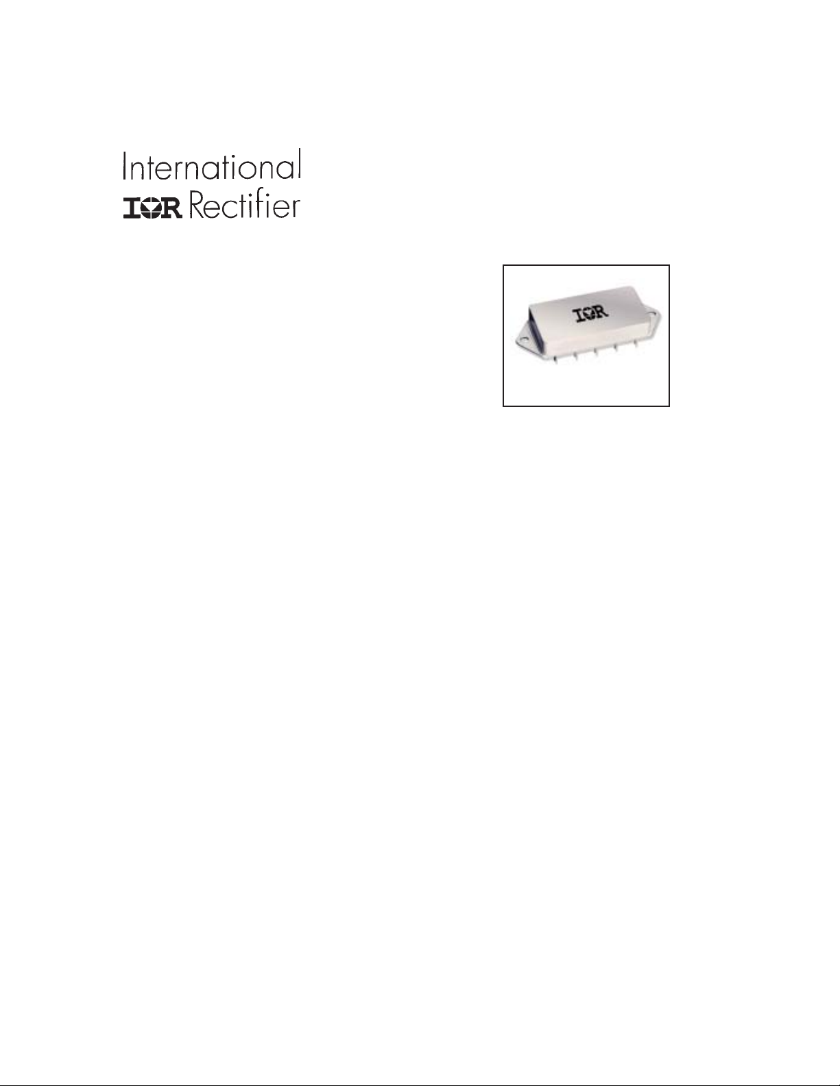
PD - 94583
AHV28XX SERIES
28V Input, Single, Dual and Triple Output
ADVANCED ANALOG
HYBRID-HIGH RELIABILITY
DC/DC CONVERTERS
Description
The AHV Series of DC/DC converters are designed to
replace the AHE/ATO family of converters in applications requiring compliance to MIL-STD-704A through
E, in particular the input surge requirement of 80 volts
specified to withstand transient input voltage of 80 volts.
No input voltage or output power derating is necessary
over the full military temperature range.
These converters are packaged in an extremely rugged, low profile package that meets all requirements of
MIL-STD-883 and MIL-PRF-38534. Parallel seam weld
sealing and the use of ceramic pin feedthru seals assure long term hermeticity after exposure to extended
temperature cycling.
The basic circuit is a push-pull forward topology using
power MOSFET switches. The nominal switching frequency is 500KHz. A unique current injection circuit
assures current balancing in the power switches. All
AHV series converters use a single stage LC input filter
to attenuate input ripple current. A low power 11.5volt
series regulator provides power to an epitaxial CMOS
custom pulse width modulator integrated circuit. This
single integrated circuit provides all PWM primary circuit functions. P o wer is transf erred from primary to secondary through a ferrite core power transformer. An
error voltage signal is generated by comparing a highly
stable reference voltage with the converter output voltage and drives the PWM through a unique wideband
magnetic feedback circuit. This proprietary feedback
circuit provides an extremely wide bandwidth, high gain
control loop, with high phase margin. The feedback
control loop gain is insensitive to temperature, radiation, aging, and variations in manufacturing. The transfer function of the feedback circuit is a function of the
feedback transformer turns ratio which cannot change
when subjected to environmental extremes.
Manufactured in a facility fully qualified to MIL-PRF38534, these converters are available in four screening grades to satisfy a wide range of requirements.
Features
n 80 Transient Input (100 msec max.)
n 50 VDC Input (Continous)
n 16 to 40 VDC Input Range
n Single, Dual and Triple Outputs
n 15 Watts Output Power
(No Temperature Derating)
n Low Input / Output Noise
n Full Military Temperature Range
n Wideband PWM Control Loop
n Magnetic Feedback
n Low Profile Hermetic Package (0.405”)
n Short Circuit and Overload Protection
n Constant Switching Frequency (500KHz)
n Tr ue Hermetic Package (Parallel Seam
Welded, Ceramic Pin Feedthru)
The CH grade is fully compliant to the requirements of MIL-PRF-38534 for class H. The HB
grade is processed and screened to the class H
requirement, but may not necessarily meet all of
the other MIL-PRF-38534 requirements, e.g., element evaluation and Periodic Inspection (P.I.)
not required. Both grades are tested to meet the
complete group “A” test specification over the full
military temperature range without output power
deration. Two grades with more limited screening are also available for use in less demanding
applications. Var iations in electrical, mechanical
and screening can be accommodated. Contact
Advanced Analog for special requirements.
www.irf.com 1
AHV
11/20/02
Page 2
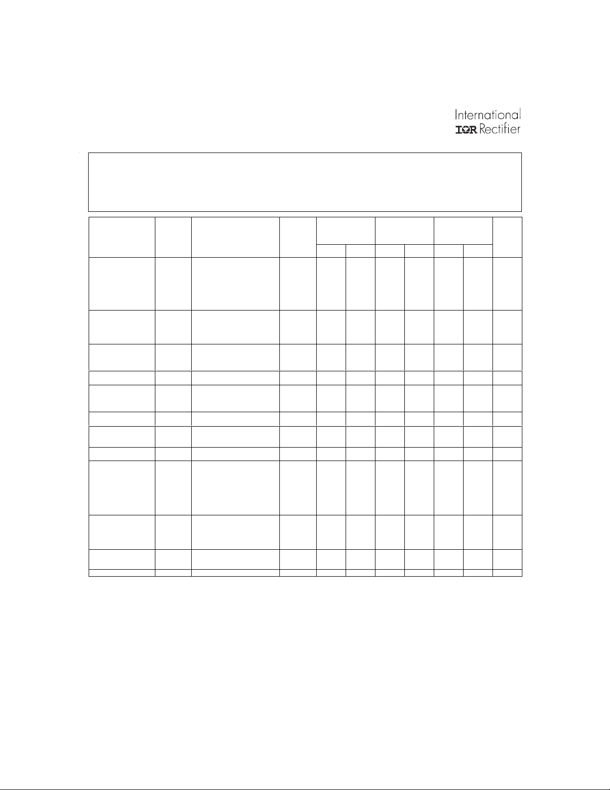
AHV28XX Series
Specifications (Single Output Models)
T
= -55°C to +125°C, V
CASE
ABSOLUTE MAXIMUM RATINGS
Input Voltage -0.5V to 50VDC (continuous) 80V (100ms)
Power Output Internally limited, 17.5W typical
Soldering 300°C for 10 seconds (1 pin at a time)
Temperature Range Operating -55°C to +135°C
Storage -65°C to +135°C
TEST
STATIC
CHARACTERISTICS
OUTPUT V
Voltage I
Current I
Ripple Voltage1 V
BW = DC to 1 MHz
Power P
REGULATION
Line
Load
INPUT
Current
Ripple Current
EFFICIENCY EFF I
ISOLATION ISO Inp ut to output or any pin to
Capacitive Load
Load Fault
Power Dissipation
2,3
C
Switching Frequency
DYNAMIC
CHARACTERISTICS
Step Load Changes
Output Transient5
5,6
Recovery
Step Line Changes
Output Transient
Recovery
TURN-ON
Overshoot
Delay
Load Fault Recovery TRLF VIN = 16 to 40 VDC 4,5,6 10 10 10 ms
Notes to Specifications (Single Output Models)
1. Bandwidth guaranteed by design. T ested f or 20 KHz to 2 MHz.
2. Capacitive load may be any value from 0 to the maximum limit without affecting dc performance. A capacitive load in excess of the maximum limit will not disturb
loop stability but will interfere with the operation of the load fault detection circuitry , appearing as a short circuit during turn-on.
3. Parameter shall be tested as part of design characterization and after design or process changes. Thereafter shall be guaranteed to the limits specified.
4. An overload is that condition with a load in excess of the rated load but less than necessary to trigger the short circuit protection and is the condition of maximum
power dissipation.
5. Load step transition time between 2 to 10 microseconds.
6. Recovery time is measured from the initiation of the transient to where V
7. Input step transition time between 2 and 10 microseconds.
8. T urn on dela y time measurement is for either a step application of pow er at input or the removal of a ground signal from the inhinbit pin (pin 2) while power is
applied to the input. Above 125°C case temperature, derate output power linearly to 0 at 135°C case.
SYMBOL
OUT
OUT
RIP
OUT
VRLINE
VRLOAD
I
IN
I
RIP
No effect on DC performance
L
P
D
F
I
S
VOT
LOAD
TT
LOAD
VOT
LINE
TT
LINE
VTon
T on D
= +28V ± 5% unless otherwise specified
IN
Condition
-55°C ≤ TC ≤ +125°C,
= 28 VDC ±5%, CL=0,
V
IN
unless otherwise specified
VIN = 16, 28, and 40 VDC 1 4.95 5.05 11.88 12.12 14.85 15.15 V
= 0 2,3 4.90 5.10 11.76 12.24 14.70 15.30 V
OUT
VIN = 16, 28, and 40 VDC 1,2,3 0.0 3.00 0.0 1.25 0.0 1.00 A
VIN = 16, 28, and 40 VDC 1,2,3 60 60 60 mVp-p
VIN = 16, 28, and 40 VDC 1,2,3 15 15 15 W
= 16, 28, and 40 VDC
V
IN
I
= 0, half load and full load
OUT
VIN = 16, 28, and 40 VDC
I
= 0, half load and full load
OUT
I
= 0, Inhibit (pin 2) = 0
OUT
= 0, Inhibit (pin 2) = Open
I
OUT
I
= Full load
OUT
= Full Load
OUT
T
= +25°C
C
case (except pin 8) at 500
VDC
TC = +25°C
TC = +25°C
Overload, TC = +25°C4
Short Circuit, TC = +25°C
= Full Load
OUT
50% Load
No Load
50% Load
No Load
50% Load
Input step 16 to 40 VDC
Input step 40 to 16 VDC
Input step 16 to 40 VDC
Input step 40 to 16 VDC
I
os
OUT
I
OUT
100% Load
135
50%
135
100%
135
50% Load
335
No lLoad
335
= OA and Full Load
= O and Full Load 8
Group A
Subgroups
1,2,3,
3,7
3,7
3,6,7
3,6,7
OUT
1
2,3
1,2,3
1,2,3
AHV2805S
Min Max Min Max Min Max Units
1 72 72 72 %
1 100 100 100
4 500 200 200
1
4
4
4
4
4
4
4
4
4
4
4,5,6
4,5,6
450 550 450 550 450 550 KHz
-300
-500
has returned to within ±1 percent of V
5
25
50
18
50
50
8.5
8.5
+300
+500
70
200
5
300
-1000
800
800
550
10
AHV2812S
30
60
120
18
50
50
8,5
8.5
-300
+300
-750
+750
70
1500
5
500
-1500
800
800
750
10
at 50 percent load.
OUT
AHV2815S
35
75
150
18
50
50
8.5
8.5
-300
+300
-750
+750
70
1500
5
500
-1500
800
800
750
10
mV
mV
mV
mA
mA
mAp-p
MΩ
µ
W
W
mVpk
mVpk
µ
µ
ms
mVpk
mVpk
µ
µ
mVpk
ms
F
s
s
s
s
2 www.irf.com
Page 3
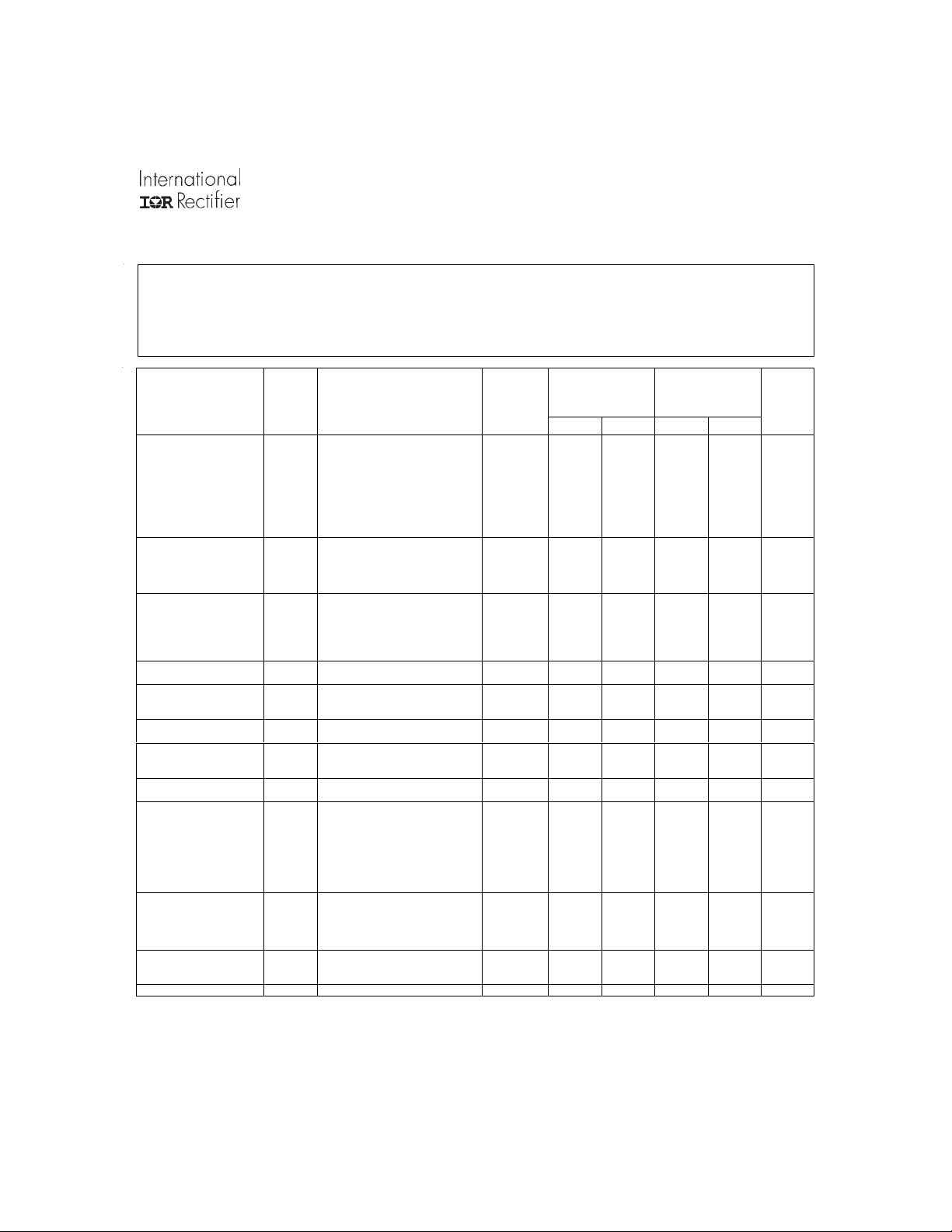
AHV28XX Series
Specifications (Dual Output Models)
T
= -55°C to +125°C, V
CASE
= +28V ± 5% unless otherwise specified
IN
ABSOLUTE MAXIMUM RATINGS
Input Voltage -0.5V to 50VDC (continuous) 80V (100ms)
Power Output Internally limited, 17.5W typical
Soldering 300°C for 10 seconds (1 pin at a time)
Temperature Range Operating -55°C to +135°C
Storage -65°C to +135°C
TEST
STATIC
CHARACTERISTICS
OUTPUT
Voltage 1 V
1,2
Current
Ripple Voltage
BW = DC to 2 MHz
Power
REGULATION
Line
Load
INPUT
Current
Ripple Current
I
1,3
V
1,2,4
P
1,5
1
3
EFFICIENCY EFF I
ISOLATION ISO Input to output or any pin to
Capacitive Load
Load Fault
Power Dissipation
6,7
C
Switching Frequency
DYNAMIC
CHARACTERISTICS
Step Load Changes
Output Transient 9
9,10
Recovery
Step Line Changes
Output Transient
Recovery
TURN-ON
Overshoot
Delay
Load Fault Recovery 7 TRLF 4,5,6 10 10 ms
7,11
7,10, 11
1
1,12
SYMBOL
I
OUT
VIN = 16, 28, and 40 VDC 1,2,3 0.0
OUT
VIN = 16, 28, and 40 VDC 1,2,3 60 60 mVp-p
RIP
VIN = 16, 28, and 40 VDC 1,2,3 15 15 W
OUT
VR
LINE
I
OUT
VR
LOAD
I
IN
I
RIP
No effect on DC performance
L
P
D
I
F
S
VOT
LOAD
TT
LOAD
VOT
LINE
TT
LINE
VTon
OS
T on D
-55°C ≤ T
V
IN
unless otherwise specified
= 0 1
OUT
= 16, 28, and 40 VDC
V
IN
= 0, half load and full load
I
OUT
VIN = 16, 28, and 40 VDC
= 0, half load and full load
I
OUT
I
= 0, Inhibit (pin 2)
OUT
Tied to input return (pin 10)
= 0, Inhibit (pin 2) = Open
I
OUT
= Full load
I
OUT
BW = DC to 2MHz
= Full Load
OUT
= +25°C
T
C
case (except pin 8) at 50 0 VD C,
TC = +25°C
TC = +25°C
Overload, TC = +25°C
Short Circuit, TC = +25°C
= Full Load
OUT
50% Load
No Load
50% Load
No Load
50% Load
Input step 16 to 40 VDC
Input step 40 to 16 VDC
Input step 16 to 40 VDC
Input step 40 to 16 VDC
= O and Full Load
I
OUT
= O and Full Load
I
OUT
Condition
≤ +125°C,
C
= 28 VDC ±5%, CL=0,
8
100% Load
135
50%
135
100%
135
50% Load
335
No lLoad
335
Group A
Subgroups
2,3
2,3
1,2,3
1,2,3
1,2,3,
4,5,6
4,5,6
AHV2812D
AHV2815D
Min Max Min Max Units
mA
mV
mV
mV
mA
mA
mAp-p
V
V
11.88
±
11.76
±
1
12.12
±
12.24
±
±
625
30
60
120
18
65
50
±
±
14.85
14.70
0.0
15.15
±
15.30
±
500
±
35
75
150
18
65
50
1 72 72 %
1 100 100
4 200 200
1
4
4
4
4
4
4
4
4
4
4
8,5
8.5
450
-300
-500
550
+300
+500
70
1500
5
1200
-1500
4
4
600
10
8.5
8.5
450
-300
-500
550
+300
+500
70
1500
5
1500
-1500
4
4
600
10
MΩ
F
µ
W
W
KHz
mVpk
mVpk
S
µ
S
µ
ms
mVpk
mVpk
s
µ
s
µ
mVpk
ms
For Notes to Specifications, refer to page 5
www.irf.com 3
Page 4

AHV28XX Series
Specifications (T riple Output Models)
T
= -55°C to +125°C, V
CASE
= +28V ± 5% unless otherwise specified
IN
ABSOLUTE MAXIMUM RATINGS
Input Voltage -0.5V to 50VDC (continuous) 80V (100ms)
Power Output Internally limited, 17.5W typical
Soldering 300°C for 10 seconds (1 pin at a time)
Temperature Range Operating -55°C to +135°C
Storage -65°C to +135°C
TEST
STATIC
CHARACTERISTICS
OUTPUT
Voltage 1 V
1,2,3
Current
Ripple Voltage
BW = DC to 2 MHz (main)
Power
REGULATION
Line
Load
INPUT
Current
Ripple Current
I
1,4
1,2,3
P
1,3
1,3
4
EFFICIENCY EFF I
ISOLATION ISO Input to output or any pin to
Capacitive Load
Load Fault
Power Dissipation
6,7
C
3
Switching Frequency 1
SYMBOL
-55°C ≤ T
V
IN
unless otherwise spec ified
Condition
≤ +125°C,
C
= 28 VDC ±5%, CL=0,
Group A
Subgroups
I
= 0 (main)
OUT
= 0 (dual)1
I
OUT
VIN = 16, 28, and 40 VDC (main) 1,2,3 0.0 2000 0.0 2000 mA
V
= 16, 28, and 40 VDC (dual)
IN
VIN = 16, 28, and 40 VDC
= 16, 28, and 40 VDC
V
IN
BW = DC to 2 MHz (main)
VIN = 16, 28, and 40 VDC (main)
(+dual)
(-dual)
(total)
= 16, 28, and 40 VDC
V
IN
= 0, 50%, and 100% load (main)
I
OUT
= 0, 50%, and 100% load (dual)
I
OUT
= 16, 28, and 40 VDC
V
IN
= 0, 50%, and 100% load (main)
I
OUT
= 0, 50%, and 100% load (dual)
I
OUT
= 0, Inhibit (pin 8)
I
OUT
Tied to input return (pin 10)
= 0
I
OUT
Inhibit (pin 2) = open
= 2000 mA (main)
I
OUT
= ±208mA (±12V)
I
OUT
= ±167mA (±15V)
I
OUT
BW = DC to 2MHz
= 2000mA (main)
OUT
= ±208mA (±12V)
I
OUT
I
= ±167mA (±15V)
OUT
case (except pin 7) at 500 VDC,
TC = +25°C
No effect on DC performance
TC = +25°C (main)
(dual)
Overload, TC = +25°C
Short Circuit, TC = +25°C
I
= 2000mA (main)
OUT
I
= ±208mA (±12V)
OUT
= ±167mA (±15V)
I
OUT
1
5
2,3
2,3
1,2,3
1,2,3
1,2,3
1,2,3
1,2,3
1,2,3
1,2,3
1,2,3
1,2,3
1,2,3
1,2,3
VR
VR
V
LOAD
I
PD
OUT
OUT
RIP
OUT
LINE
I
IN
RIP
L
F
S
AHV2812T
AHV2815T
Min Max Min Max Units
1
1
4.95
4.90
11.88
±
11.76
±
0.0
10
2.5
2.5
15
5.05
5.10
12.12
±
12.24
±
208
±
80
40
10
25
60
±
50
60
±
15
50
50
4.95
4.90
14.85
±
14.70
±
0.0
2.5
2.5
15
5.05
5.10
15.15
±
15.30
±
167
±
80
40 mVp-p
W
25
75
±
50
75
±
15
50
50
mA
mVp-p
W
W
W
mV
mV
mV
mV
mA
mA
mAp-p
V
V
V
V
1 72 72 %
1 100 100
4
1
1
4
500
200
8.5
8.5
450
550
500
200
8.5
8.5
450
550
MΩ
F
µ
F
µ
W
W
KHz
For Notes to Specifications, refer to page 5
4 www.irf.com
Page 5

AHV28XX Series
Specifications (T riple Output Models) - continued
TEST
DYNAMIC
CHARACTERISTICS
Step Load Changes
Output Transient
Recovery
Step Line Changes
Output Transient
Recovery
TURN-ON
Overshoot 1
Delay
9
9,10
7,10, 11
1,12
Load Fault Recovery 7 TRLF 4 15 15 ms
Notes to Specifications (Tr iple Output Models)
SYMBOL
VOT
LOAD
TT
LOAD
VOT
LINE
TT
LINE
VTon
OS
T on D
-55°C ≤ T
VIN = 28 VDC ±5%, CL=0,
unless otherwise specified
50% Load
No Load
50% Load
No Load
50% Load
Input step 16 to 40 VDC
Input step 40 to 16 VDC
Input step 16 to 40 VDC
Input step 40 to 16 VDC
= O and ±625mA
I
OUT
= O and ±625mA
I
OUT
Condition
100% Load
135
50%
135
100%
135
50% Load
335
No lLoad
335
≤ +125°C,
C
Group A
Subgroups
AHV2812T
Min Max Min Max Units
4
4
4
4
4
4
4
4
4
4
4
-300
-400
1. Tested at each output.
2. Parameter guaranteed by line and load regulation tests.
3. At least 25 percent of the total power should be taken from the (+5 volt) main output.
4. Bandwidth guaranteed by design. Tested for 20KHz to 2MHz.
5. An overload is that condition with a load in excess of the rated load but less than that necessary to trigger the short circuit
protection and is the condition of maximum power dissipation.
6. Capacitive load may be any value from 0 to the maximum limit without affecting dc performance. A capacitive load in excess of the
maximum limit will not disturb loop stability but may interfere with the operation of the load fault detection circuitry, appearing as a
short circuit during turn-on.
7. Parameter shall be tested as part of design characterization and after design or process changes. Thereafter parameters shall be
guaranteed to the limits specified.
8. Above 125°C case temperature, derate output power linearly to 0 at 135 °C case.
9. Load step transition time between 2 and 10 microseconds.
10. Recovery time is measured from the initiation of the transient to where V
load.
has returned to within ±1 percent of V
OUT
11. Input step transition time between 2 and 10 microseconds.
12. Turn on delay time measurement is for either a step application of power at input or the removal of a ground signal from the inhibit
pin (pin 8) while power is applied to the input.
+300
+400
100
2000
5
1200
-1500
4
4
750
15
AHV2815T
-300
-400
+300
+400
100
2000
5
1200
-1500
4
4
750
15
OUT
mVpk
mVpk
S
µ
S
µ
ms
mVpk
mVpk
s
µ
s
µ
mVpk
ms
at 50 percent
Notes to Specifications (Dual Output Models)
1. Tested at each output.
2. Parameter guaranteed by line and load regulation tests.
3. Bandwidth guaranteed by design. Tested for 20KHz to 2MHz.
4. Total power at both outputs.
5. When operating with unbalanced loads, at least 25% of the load must be on the positive output to maintain regulation.
6. Capacitive load may be any value from 0 to the maximum limit without affecting dc performance. A capacitive load in excess of the
maximum limit will not disturb loop stability but may interfere with the operation of the load fault detection circuitry, appearing as a
short circuit during turn-on.
7. Parameter shall be tested as part of design characterization and after design or process changes. Thereafter parameters shall be
guaranteed to the limits specified.
8. An overload is that condition with a load in excess of the rated load but less than that necessary to trigger the short circuit
protection and is the condition of maximum power dissipation.
9. Load step transition time between 2 and 10 microseconds.
10. Recovery time is measured from the initiation of the transient to where V
load.
has returned to within ±1 percent of V
OUT
at 50 percent
OUT
11. Input step transition time between 2 and 10 microseconds.
12. Turn on delay time measurement is for either a step application of power at input or the removal of a ground signal from the inhibit
pin (pin 2) while power is applied to the input.
13. Above 125°C case temperature, derate output power linearly to 0 at 135°C.
www.irf.com 5
Page 6

AHV28XX Series
p
AHV28XX (Single Output) Block Diagram
5
+Vout
1
+Input
8
Case
2
Enable
Input
Return
10
1
+Input
2
Enable
8
Case
Input
Return
10
EMI
Filt e r
EMI
Filt er
Drive 1
Pulse Width
Modulator
FB
Drive 2
AHV28XX (Dual Output) Block Diagram
Drive 1
Pulse Width
Modulator
FB
Drive 2
Error
Amp &
Ref
Error Am p
& Reference
Regulator
Return4
V
3
ADJ
3
+Vout
Return
4
-Vout
5
AHV28XX (T riple Output) Block Diagram
5
+Vout
Regulator
4
-Vout
+5V out
2
3
Return
1
+Input
8
Enable
7
Case
Input
Return
EMI
Filter
Pulse
Width
Modulator
Drive 1
Drive 2
FB
Erro r A m
& R e fe re n ce
10
6 www.irf.com
Page 7

Application Information
Inhibit Function
Connecting the inhibit pin (Pin 2 of single and dual models,
pin 8 of triple models) to the input return (pin 10) will cause
the converter to shutdown and operate in a low power
standby mode. Power consumption in this mode is calculated by multiplying Vin times the input current inhibited,
typically 225mW at Vin equal to 28 volts. The input current
inhibited is relatively constant with changes in Vin. The open
circuit inhibit pin voltage is typically 11.5 volts and can be
conveniently driven by an open collector driver. An inter nal
pull-up resistor enables the user to leave this pin floating if
the inhibit function is not used in their particular application.
All models use identical inhibit internal circuits. Forcing inhibit pin to any voltage between 0 and 6 volts will assure the
converter is inhibited. The input current to this pin is 500µA
maximum at Vpin2 = to 0 volts. The converter can be turned
on by opening Pin 2 or forcing a voltage from 10 to 50 volts.
Inhibit pin current from 10 to 50 volts is less than ±50µA.
AHV28XX Series
EMI Filter
An optional EMI filter ( AFC461) will reduce the input ripple
current to levels below the limits imposed by MIL-STD461 CEO3.
The output voltage of the AHV28XXS can be adjusted
upward by connecting a resistor between the Output
Adjust (Pin 3) and the Output Common (Pin 4) as shown
in T ab le 1.
Table 1: Output Adjustment Resistor Values
Pin 3 to 4
None 0 0 0
390 K +1.0% +1.6% +1.7%
145 K +2.0% +3.2% +3.4%
63 K +3.1% +4.9% +5.1%
22 K +4.1% +6.5% +6.8%
0 +5.0% +7.9% +8.3%
* Output Adjust (Single Output Models Only)
Output Voltage Increase (%) * Resistance (Ohms)
5V 12V 15V
www.irf.com 7
Page 8

AHV28XX Series
yp
yp
0
p
p
AHV28XX Case Outlines
Single and Dual Output Models
0.050
ical
T
0.040 D X
0.26 L Pins
0.800
123 54
2.880
Max
1.110
2.560
2.110
Max
0.405
Max
T riple Output Models
1.000
123 54
610987
0.410
Max
Pin Designation
SIGNAL DESIGNATION
PIN # SINGLE OUTPUT DUAL OUTPUT
1 Positive Input P os i t iv e I nput Positive Input
2 Enable Input Enable Input +5VDC Output
3 Output Adjust* Positive Output Output Common
4 Output Common Output Common Neg. Dual Output (12/15 VDC )
5 Positive Output Negative Output Pos. Dual Output (12/15 VDC)
6 N/C N/C N/C
7 N/C N/C Case Ground
8 Case Ground Case Ground Enable Input
9 N/C N/C N/C
10 Input Common Input Common Input Common
TRIPLE OUTPUT
4 X 0.400
=1.600
610987
Ø 0.162
2 Holes
ical
T
2.360
1.95
1.345
Part Numbering
AHV 28 15 T F / CH
Model
Input Voltage
28 = 28V Nominal
Output Voltage
Single - 05, 12, 15V
Dual - 12 = ±12V, 15 = ±15V
Tri
le - 12 = 5V, ±12V
15 = 5V, ±15V
2.70
Max
Screening
–
, ES, HB, CH
Package Style
F = Flange
Outputs
S = Single
D = Dual
T = Tri
le
* Output Adjust (Single Output Models Only)
8 www.irf.com
Page 9

Availab le Screening Levels and Process Variations for AHV28XX Series
AHV28XX Series
Requirement
Temperature Range -20°C to +85°C -55°C to +125°C -55°C to +125°C -55°C to +125°C
Element Evaluation MIL-PRF-38534
Internal Visual 2017
Temperature Cycle 1010 Cond B Cond C Cond C
Constant Ac celeration 2001 500g Cond A Cond A
Burn-in 1015 48hrs @ 85°C 48hrs @ 125°C 160hrs @ 125° C 160hrs @ 125°C
Final Electri cal
(Group A)
Seal, Fine & Gross 1014 Cond A Cond A, C Cond A, C Cond A, C
External Visual 2009
* Per Commercial Standards
MIL-STD-883
Method
MIL-PRF-38534
& Specification
No
Suffix
¬
25°C 25°C -55 , +25, +125°C -55, +25, +125°C
¬
ES
Suffix
Yes Yes Yes
Yes Yes Yes
HB
Suffix
CH
Suffix
Availab le Standard Military Drawing (SMD) Cross Reference
Standardized
Military Drawing
Pin
AHV2805SF/CH
AHV2812SF/CH
AHV2815SF/CH
AHV2812DF/CH
AHV2815DF/CH
AHV2812TF/CH
AHV2815TF/CH
Vendor
CAGE
Code
52467
52467
52467
52467
52467
52467
52467
Vendor
Similar
Pin
5962-9177301
5962-9211201
5962-9211301
5962-9211401
5962-9177401
5962-9211501
5962-9211601
WORLD HEADQUARTERS: 233 Kansas St., El Segundo, California 90245, Tel: (310) 322 3331
ADVANCED ANALOG: 2270 Martin Av., Santa Clara, California 95050, Tel: (408) 727-0500
Visit us at www.irf.com for sales contact information.
Data and specifications subject to change without notice. 11/02
www.irf.com 9
 Loading...