

Page 1
PD55025
PD55025S
RF POWER TRANSISTORS
N-CHANNEL ENHANCEMENT-MODE LATERAL
MOSFETs
• EXCELLENT THERMAL STABILITY
• COMMON SOURCE CONFIGURATION
• P
= 25 W with 14.5 dB gain @ 500 MHz /
OUT
12.5 V
• NEW RF PLASTIC PACKAGE
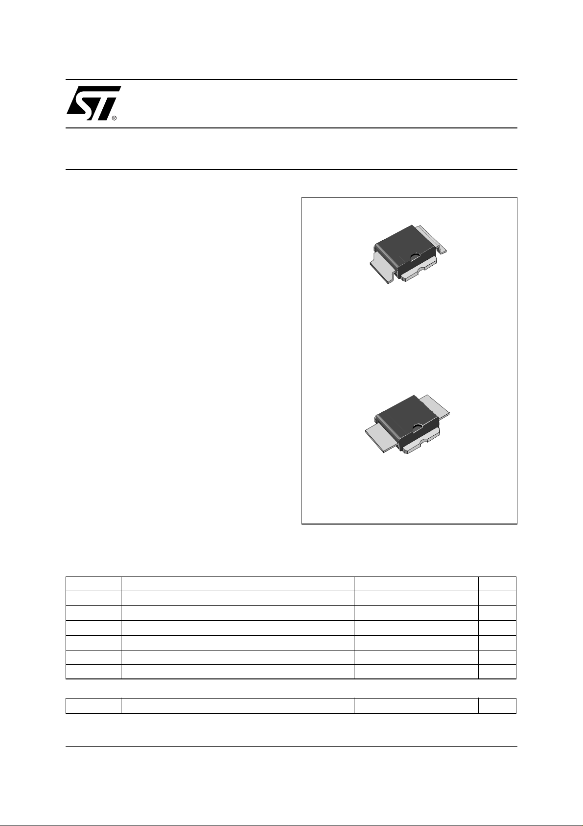
DESCRIPTION
The PD55025 is a common source N-Channel,
enhancement-mode lateral Field-Effect RF power
transistor. It is designed for high gain, broad band
commercial and industrial applications. It operates
at 12 V in common source mode at frequencies of
up to 1 GHz. PD 55025 boasts the excellent gain,
linearity and reliability of ST’s latest LDMOS
technology mounted in the first true SMD pla stic
RF power package, PowerSO-10RF . PD55025’s
superior linearity performance makes it an ideal
solution for car mobile radio.
The LdmoST
PowerSO-10RF
(formed lead)
ORDER CODE
PD55025
Plastic FAMILY
BRANDING
PD55025
The PowerSO-10 plastic package, designed to
offer high reliability, is the first ST JEDEC
approved, high power SM D package. I t has b een
specially optimized for RF needs and offers
excellent RF performances and ease of assembly.
ORDER CODE
PD55025S
PowerSO-10R F
(straight lead)
BRANDING
PD55025S
Mounting recommendations are available in
www.st.com/rf/ (look for application note AN1294)
ABSOLUTE MAXIMUM RATINGS (T
Symbol Parameter Value Unit
V
(BR)DSS
V
GS
I
D
P
DISS
Tj Max. Operating Junction Temperature 165 °C
T
STG
Drain-Source Voltage 40 V
Gate-Source Voltage ± 20 V
Drain Current 7 A
Power Dissipation (@ Tc = 70°C) 79 W
Storage Temperature -65 to +150 °C
CASE
= 25°C)
THERMA L D ATA
R
th(j-c)
Junction -Case Thermal Resistance 1.2 °C/W
1/13March, 21 2003
Page 2
PD55025 - PD55025S
ELECTRICAL SPECIFICATION (T
CASE
= 25°C)
STATIC
Symbol Test Conditions Min. Typ. Max. Unit
I
DSS
I
GSS
V
GS(Q)
V
DS(ON)
G
C
C
C
FS
ISS
OSS
RSS
VGS = 0 V VDS = 28 V
VGS = 20 V VDS = 0 V
VDS = 28 V
= 100 mA
ID
VGS = 10 V ID = 3 A
VDS = 10 V ID = 3 A
VGS = 0 V VDS = 12.5 V f = 1 MHz
VGS = 0 V VDS = 12.5 V f = 1 MHz
VGS = 0 V VDS = 12.5 V f = 1 MHz
1 µA
1 µA
2.0 5.0 V
0.7 0.8 V
2.5 mho
86 pF
76 pF
5.8 pF
DYNAMIC
Symbol Test Conditions Min. Typ. Max. Unit
P
out
G
P
η
D
Load
mismatch
VDD = 12.5 V IDQ = 200 mA f = 500 MHz
VDD = 12.5 V IDQ = 200 mA P
VDD = 12.5 V IDQ = 200 mA P
= 12.5 V IDQ = 200 mA P
V
DD
= 25 W f = 500 MHz
OUT
= 25 W f = 500 MHz
OUT
= 25 W f = 500 MHz
OUT
ALL PHASE ANGLES
25 W
14.5 dB
50 %
20:1 VSWR
GATE
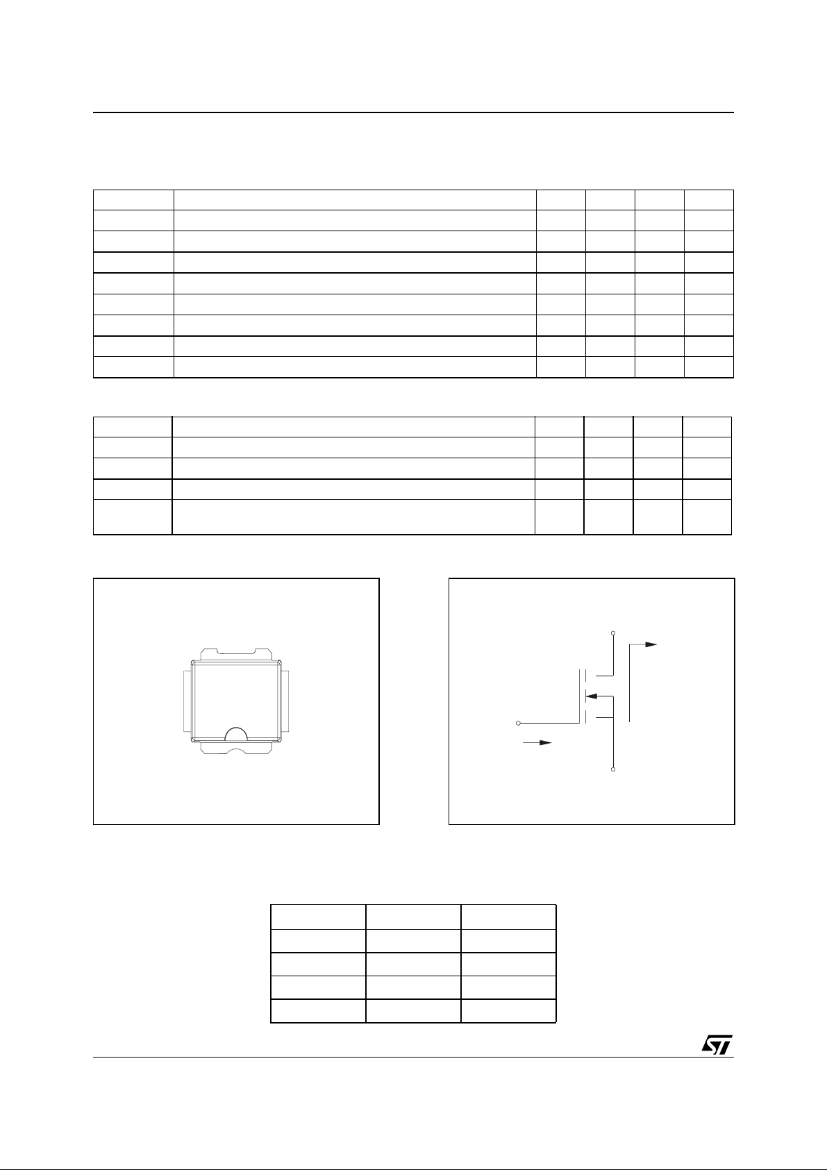
SC15200
PIN CONNECTION
PD55025S
SOURCE
DRAIN
SC13140
IMPEDANCE DATA
Z
FREQ. MHz
175 3.20 - j 4.41 1.56 + j 2.14
480 1.01 - j 1.67 1.06 + j 0.22
500 0.93 - j 1.53 1.12 + j 0.20
(Ω)Z
IN
Typical Input
Impeda nce
G
Zin
(Ω)
DL
D
Z
Typical Drain
Load Imped ance
S
DL
2/13
520 0.88 - j 1.98 1.07 + j 0.83
Page 3
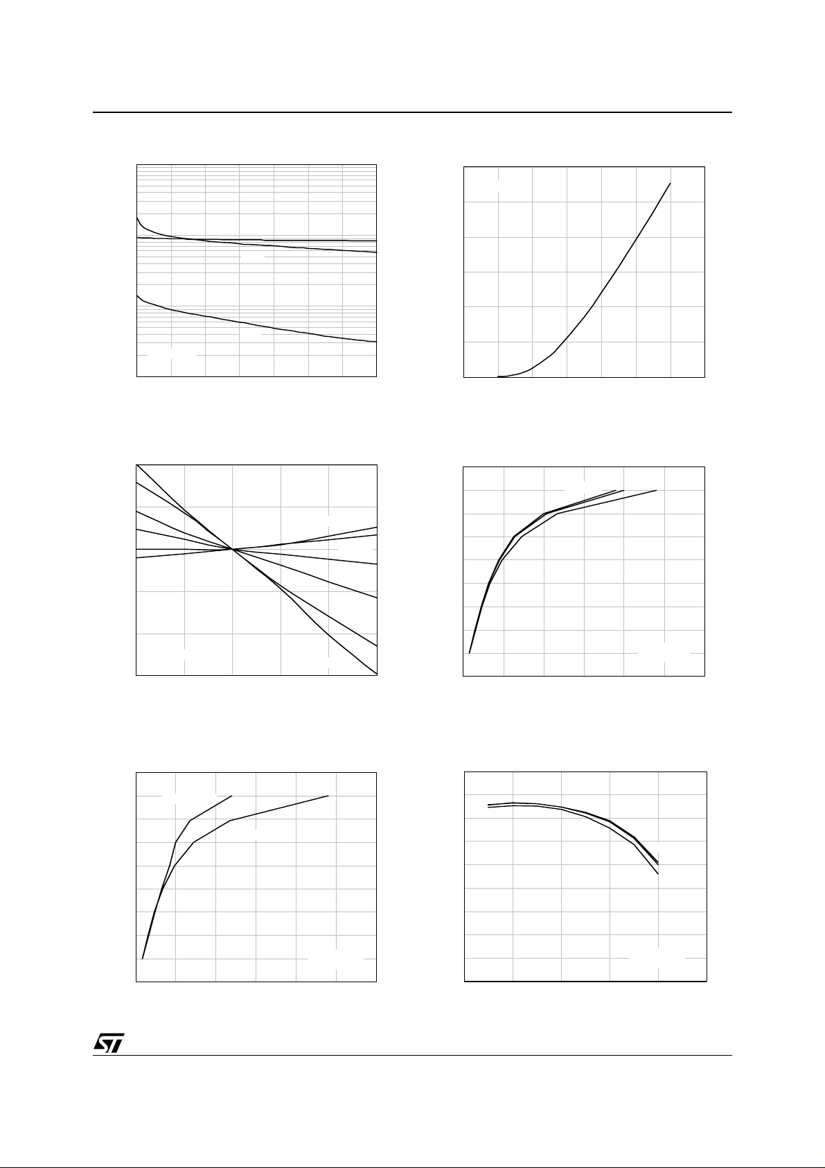
TYPICAL PERFORMANCE
q
Capacitance vs. Supply Voltage
1000
Ciss
100
Coss
C (pF)
(PD55025S)
PD55025 - PD55025S
Drain Current vs Gate-Source Voltage
6
Vds = 10 V
5
4
3
Id (A)
10
Crss
f = 1 MHz
1
0 4 8 1216202428
Vds (V)
Gate-Source Voltage vs Case Temperature
1.04
1.02
Id = 5 A
1.00
Id (A)
0.98
0.96
Vds = 10 V
0.94
-25 0 25 50 75 100
Vgs (V)
Id = 4 A
Id = 3 A
Id = 2 A
Id = 1 A
Id = .5 A
2
1
0
2.0 2.5 3.0 3.5 4.0 4.5 5.0 5.5
Vgs (V)
Output Power vs Input Power
45
40
35
30
25
20
Pout (W)
15
10
5
0
0.00 1.00 2.00 3.00 4.00 5.00 6.00
480 MH z
Pin (W)
500 MHz
520 MHz
Vdd = 12.5 V
Id
= 200 mA
Output Power vs Input Power
45
40
35
30
25
20
Pout (W)
15
10
Vdd = 13.8 V
Vdd = 12 .5 V
5
0
0123456
Pin (W)
f = 520 MHz
Idq = 200 mA
Powe r Ga i n vs Outpu t Pow er
18
16
14
12
10
Gp (dB)
8
6
4
2
0
0 1020304050
Pout (W)
520 MHz
Vdd = 12.5 V
Idq = 200 mA
480 MHz
500 MHz
3/13
Page 4
PD55025 - PD55025S
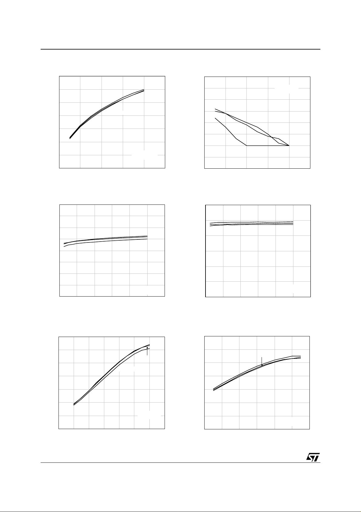
TYPICAL PERFORMANCE
Drain Efficiency vs Output Power
(PD55025S)
Input Return Loss vs Output Power
70
60
50
40
Nd (%)
30
20
10
0
0 1020304050
500 MHz
480, 520 MHz
Pout (W)
Vdd = 12.5 V
Idq = 200 mA
Output Power vs Bias Curent
40
35
30
25
20
Pout (W)
15
10
5
0
0 200 400 600 800 100 0 1200
Idq (m A)
480 MHz
520 MHz
Vdd = 12.5 V
Pin = 0.85 W
500 MHz
0
-5
-10
-15
-20
RL (dB)
-25
-30
-35
-40
0 1020304050
480 MHz
500 MHz
520 MHz
Pout (W)
Vdd = 12.5 V
Idq = 200 mA
Drain Efficiency vs Bias Current
60
50
40
30
Nd (%)
20
10
0
0 200 400 600 800 1000 1200
Idq ( m A)
500 MHz
520 MHz
Vdd = 12.5 V
Pin = 0 . 85 W
480 MH z
Output Power vs Supply Voltage
35
30
25
20
Pout (W)
15
10
5
0
5 7 9 1113151719
Vdd ( V)
4/13
520 MHz
480 MHz
500 MHz
I dq = 200 mA
Pin = 0.85 W
Drain Efficiency vs Supply Voltage
70
60
50
40
Nd (%)
30
20
10
0
6 8 10 12 14 16 18
500 MHz
500 MHz
520 MHz
Vdd (V)
Idq = 200 mA
Pin = 0.85 W
Page 5

TYPICAL PERFORMANCE
g
)
(PD55025S)
Output Power vs Gate-Source Voltage
PD55025 - PD55025S
Output Power vs Input Power (f = 175 MHz)
30
25
20
15
Pout (W)
500 MHz
10
5
0
01234
480 MHz
520 MHz
V
s (V
Vdd = 12.5 V
Pin = 0.85 W
Power Gain vs Output Power (f = 175 MHz)
30
25
20
45
40
35
30
25
Pout (W)
20
15
10
5
0
0 0.5 1 1.5 2 2.5
Pin (W)
Vdd = 12.5 V
I dq = 200 mA
Drain Efficiency vs Output Power (f = 175 MHz)
80
70
60
50
15
Gp (W)
10
5
0
0 1020304050
Pout (W)
Vdd = 12.5 V
Idq = 200 mA
Input Return Loss vs Output Power (f = 175 MHz)
0
-5
-10
-15
RL (dB)
-20
-25
Vdd = 12.5 V
Idq = 200 mA
40
Nd (%)
30
20
10
0
0 1020304050
Pout (W)
Vdd = 12.5 V
Idq = 200 m A
-30
0 1020304050
Pout (W)
5/13
Page 6

PD55025 - PD55025S
500 MHz TEST CIRCUIT SCHEMATIC (ENGINEERING)
VGG
B1
B2
+
+
C10
RF
INPUT
C9
C1
R3
C8
Z2
Z1 Z3
C2
C3
R2
R1
C4
C5
C7
Z4
C6
DUT
C19
L1
Z6
Z5
C12
Z7
C11
C18 C17 C16
Z9
C14
C15
Z8
C13
N2
OUTPUT
RF
500 MHz TEST CIRCUIT COMPONENT PART LIST
COMPONENT DESCRIPTIO N
B1,B2 FERRITE BEAD
C1,C13 300 pF, 100 mil CHIP CAPACITOR
C2,C3,C4,C12,C13,C14 1 to 20 pF TRIMMER CAPACITOR
C6 39 pF ATC 100B SURFACE MOUNT CERAMIC CHIP CAPACITOR
C7, C19 120 pF 100 mil CHIP CAPACITOR
C10, C16 10 µF, 50 V ELECTROLYTIC CAPACITOR
C9, C17 0.1 mF, 100 mil CHIP CAP
C8, C18 1.000 pF 100 mil CHIP CAP
C5, C11 33 pF, 100 mil CHIP CAP
L1 56 nH, 7 TURN, COILCRAFT
N1, N2 TYPE N FLANGE MOUNT
R1 15 Ω, 1 W CHIP RESISTOR
R2 1 KΩ, 1 W CHIP RESISTOR
R3 33 KΩ, 1 W CHIP RESISTOR
Z1 0.471” X 0.080” MICROSTRIP
Z2 1.082” X 0.080” MICROSTRIP
Z3 0.372” X 0.080” MICROSTRIP
Z4,Z5 0.260” X 0.223” MICROSTRIP
Z6 0.050” X 0.080” MICROSTRIP
Z7 0.551” X 0.080” MICROSTRIP
Z8 0.825” X 0.080” MICROSTRIP
Z9 0.489” X 0.080” MICROSTRIP
BOARD
ROGER, ULTRA LAM 2000 THK 0.030”,
εr = 2.55 2oz. ED cu 2 SIDES.
VDD
6/13
Page 7

500 MHz TEST CIRCUIT
PD55025 - PD55025S
500 MHz TEST CIRCUIT PHOTOMASTER
BIAS
VDD
GND
6.4 inches
4 inches
7/13
Page 8

PD55025 - PD55025S
175 MHz TEST CIRCUIT SCHEMATIC (ENGINEERING)
FB2FB1
C16
C16
FB2FB1
L1
L1
R5
R5
+
+
V
V
GG
GG
C8
C8
)
))
RF
RF
INPUT
INPUT
C9
C9
C1
C1
C10
C10
R1
R1
R2
R2
C14
C14
C15
C15
R3
R3
C2
C2
C3
C3
R4
R4
C7
C7
175 MHz TEST CIRCUIT COMPONENT PART LIST
COMPONENT DESCRIPTION
C1, C6 300 pF CHIP CAPACITOR
C2, C3 91 pF CHIP CAPACITOR
C4, C14 75 pF CHIP CAPACITOR
C5 1-20 pF TRIMMER CAPACITOR
C7 .01 µF MOLDED CAPACITOR
C8, C13 10 µF ELECTROLYTIC CAPACITOR
C9, C12 .1 µF CHIP CAPACITOR
C10, C11 1000 pF CHIP CAPACITOR
C15, C16 1200 pF CHIP CAPACITOR
FB1, FB2 FERRITE BEAD
R1 33 KΩ CHIP RESISTOR
R2 17 Ω CHIP RESISTOR
R3 15 Ω CHIP RESISTOR
R4 47 Ω CHIP RESISTOR
R5 220 Ω CHIP RESISTOR
L1 5 TURN, 16 AWG MAGNET WIRE, ID = .40” ,INDUCTOR
BOARD
ROGER, ULTRA LAM 2000, THK 0.030”,
εr = 2.55 2oz. ED cu 2 SIDES.
C11 C12
C11 C12
C4 C5
C4 C5
+
+
V
V
DD
DD
C13
C13
)
)
C6
C6
RF
RF
OUTPUT
OUTPUT
8/13
Page 9

PD55025 - PD55025S
COMMON SOURCE S-PARAMETER (PD55025S)
= 12.5 V ID = 500 mA)
(V
DS
FREQ
IS11I
∠Φ
S
11
IS
I
21
∠Φ
S
21
(MHz)
50 0.837 -162 13.33 89 0.018 -1 0.780 -168
100 0.846 -169 6.51 76 0.017 -12 0.803 -172
150 0.862 -171 4.15 66 0.016 -19 0.831 -172
200 0.878 -173 2.93 58 0.015 -26 0.859 -172
250 0.895 -174 2.20 51 0.013 -31 0.874 -172
300 0.910 -174 1.71 45 0.012 -36 0.886 -173
350 0.921 -175 1.36 40 0.010 -40 0.892 -173
400 0.932 -176 1.11 35 0.009 -42 0.897 -175
450 0.941 -177 0.92 31 0.008 -43 0.915 -176
500 0.946 -178 0.78 27 0.007 -44 0.932 -177
550 0.953 -178 0.66 24 0.006 -43 0.946 -178
600 0.957 -179 0.57 21 0.005 -42 0.964 -179
650 0.960 -180 0.50 18 0.004 -39 0.975 -178
700 0.964 180 0.44 16 0.004 -34 0.976 -179
750 0.966 179 0.39 14 0.003 -29 0.981 -179
800 0.968 178 0.95 12 0.002 -15 0.979 -179
850 0.970 178 0.31 10 0.002 -2 0.964 -179
900 0.971 177 0.28 8 0.002 16 0.960 180
950 0.972 177 0.26 6 0.002 34 0.953 179
1000 0.972 176 0.23 5 0.003 45 0.940 178
IS
I
12
∠Φ
S
12
IS
I
22
∠Φ
S
22
COMMON SOURCE S-PARAMETER (PD55025S)
(V
= 12.5 V ID = 1.5 A)
DS
FREQ
IS11I
∠Φ
S
11
IS
I
21
∠Φ
S
21
(MHz)
50 0.876 -164 13.87 90 0.013 1 0.823 -172
100 0.880 -172 6.87 79 0.012 -7 0.838 -175
150 0.887 -174 4.46 71 0.012 -13 0.855 -176
200 0.895 -175 3.22 64 0.011 -18 0.873 -175
250 0.905 -176 2.47 58 0.010 -22 0.879 -175
300 0.915 -176 1.96 52 0.009 -25 0.885 -175
350 0.922 -177 1.60 47 0.009 -28 0.886 -175
400 0.931 -178 1.32 42 0.008 -30 0.889 -177
450 0.938 -178 1.11 38 0.007 -31 0.906 -178
500 0.942 -179 0.95 34 0.006 -31 0.923 -179
550 0.948 -179 0.82 31 0.005 -30 0.937 -179
600 0.952 -180 0.71 28 0.005 -27 0.956 -179
650 0.954 180 0.63 25 0.004 -22 0.967 -179
700 0.959 179 0.55 22 0.003 -16 0.969 -179
750 0.961 178 0.49 20 0.003 -6 0.973 -179
800 0.963 178 0.45 17 0.003 3 0.970 -179
850 0.966 177 0.40 15 0.003 17 0.956 -180
900 0.967 177 0.36 13 0.003 27 0.952 179
950 0.968 176 0.33 11 0.003 38 0.945 179
1000 0.968 176 0.30 9 0.003 45 0.933 177
IS
I
12
∠Φ
S
12
IS
I
22
∠Φ
S
22
9/13
Page 10

PD55025 - PD55025S
COMMON SOURCE S-PARAMETER (PD55025S)
= 12.5 V ID = 3 A)
(V
DS
FREQ
IS11I
∠Φ
S
11
IS
I
21
∠Φ
S
21
(MHz)
50 0.890 -165 13.19 91 0.012 2 0.837 -174
100 0.892 -172 6.55 81 0.011 -6 0.846 -176
150 0.898 -174 4.28 73 0.011 -12 0.865 -176
200 0.904 -175 3.11 66 0.010 -15 0.879 -176
250 0.913 -176 2.39 60 0.010 -20 0.883 -176
300 0.921 -177 1.91 54 0.009 -23 0.089 -176
350 0.926 -177 1.57 49 0.008 -25 0.887 -176
400 0.935 -178 1.31 44 0.007 -27 0.889 -177
450 0.941 -179 1.10 40 0.007 -28 0.905 -179
500 0.944 -179 0.94 36 0.006 -27 0.921 -179
550 0.949 -180 0.82 33 0.005 -25 0.936 -180
600 0.953 180 0.71 29 0.004 -21 0.954 180
650 0.955 179 0.63 26 0.004 -17 0.964 -180
700 0.959 179 0.56 24 0.003 -10 0.965 -180
750 0.961 178 0.50 21 0.003 -2 0.968 -180
800 0.963 177 0.45 19 0.003 10 0.966 -179
850 0.966 177 0.41 17 0.003 22 0.952 -180
900 0.967 176 0.37 15 0.003 32 0.948 180
950 0.968 176 0.34 15 0.003 41 0.942 179
1000 0.969 175 0.31 11 0.004 49 0.930 177
IS
I
12
∠Φ
S
12
IS
I
22
∠Φ
S
22
COMMON SOURCE S-PARAMETER
(V
= 13.8 V ID = 3 A)
DS
FREQ
IS11I
∠Φ
S
11
(PD55025S)
IS
I
21
IS
∠Φ
S
21
I
12
∠Φ
S
12
IS
I
22
(MHz)
50 0.849 -164 13.99 91 0.012 2 0.833 -173
100 0.881 -171 6.94 80 0.011 -6 0.841 -175
150 0.895 -173 4.51 72 0.011 -12 0.857 -175
200 0.903 -175 3.27 65 0.010 -16 0.871 -175
250 0.912 -176 2.50 58 0.010 -21 0.877 -175
300 0.921 -176 1.99 52 0.009 -24 0.882 -175
350 0.927 -177 1.62 47 0.008 -27 0.883 -176
400 0.936 -178 1.35 42 0.007 -29 0.886 -177
450 0.943 -178 1.13 38 0.006 -29 0.904 -178
500 0.946 -179 0.97 34 0.006 -29 0.920 -179
550 0.952 -180 0.83 31 0.005 -26 0.935 -179
600 0.955 180 0.72 27 0.004 -23 0.955 -180
650 0.957 179 0.64 24 0.004 -17 0.965 -179
700 0.961 179 0.56 22 0.003 -8 0.967 -179
750 0.963 178 0.50 19 0.003 2 0.970 -179
800 0.965 178 0.45 17 0.003 14 0.968 -179
850 0.968 177 0.41 15 0.003 27 0.953 -179
900 0.969 176 0.37 13 0.003 36 0.949 180
950 0.970 176 0.34 11 0.003 45 0.943 179
1000 0.971 175 0.31 9 0.003 54 0.930 178
∠Φ
S
22
10/13
Page 11

PD55025 - PD55025S
PowerSO-10RF Straight Lead MECHANICAL DATA
DIM.
A1 1.62 1.67 1.72 0.064 0.065 0.068
A2 3.4 3.5 3.6 0.134 0.137 0.142
A3 1.2 1.3 1.4 0.046 0.05 0.054
A4 0.15 0.2 0.25 0.005 0.007 0.009
a 0.2 0.007
b 5.4 5.53 5.65 0.212 0.217 0.221
c 0.23 0.27 0.32 0.008 0.01 0.012
D 9.4 9.5 9.6 0.370 0.374 0.377
D1 7.4 7.5 7.6 0.290 0.295 0.298
E 15.15 15.4 15.65 0.595 0.606 0.615
E1 9.3 9.4 9.5 0.365 0.37 0.375
E2 7.3 7.4 7.5 0.286 0.292 0.294
E3 5.9 6.1 6.3 0.231 0.24 0.247
F 0.5 0.019
G 1.2 0.047
R1 0.25 0.01
R2 0.8 0.031
T1 6 deg 6 deg
T2 10 deg 10 deg
MIN. TYP. MAX MIN. TYP. MAX
mm Inch
Note (1): Resin protrusions not included (max value: 0.15 mm per side)
CRITICAL DIMENSIONS:
- Overall width (L)
11/13
Page 12

PD55025 - PD55025S
PowerSO-10RF Formed Lead (Gull Wing) MECHANICAL DATA
DIM.
A1 0 0.05 0.1 0. 0.0019 0.0038
A2 3.4 3.5 3.6 0.134 0.137 0.142
A3 1.2 1.3 1.4 0.046 0.05 0.054
A4 0.15 0.2 0.25 0.005 0.007 0.009
a 0.2 0.007
b 5.4 5.53 5.65 0.212 0.217 0.221
c 0.23 0.27 0.32 0.008 0.01 0.012
D 9.4 9.5 9.6 0.370 0.374 0.377
D1 7.4 7.5 7.6 0.290 0.295 0.298
E 13.85 14.1 14.35 0.544 0.555 0.565
E1 9.3 9.4 9.5 0.365 0.37 0.375
E2 7.3 7.4 7.5 0.286 0.292 0.294
E3 5.9 6.1 6.3 0.231 0.24 0.247
F 0.5 0.019
G 1.2 0.047
L 0.8 1 1.1 0.030 0.039 0.042
R1 0.25 0.01
R2 0.8 0.031
T 2 deg 5 deg 8 deg 2 deg 5 deg 8 deg
T1 6 deg 6 deg
T2 10 deg 10 deg
Note (1): Resin protrusions not included (max value: 0.15 mm per side)
MIN. TYP . MAX MIN. TYP . MAX
mm Inch
12/13
CRITICAL DIMENSIONS:
- Stand-off (A1)
- Overall width (L)
Page 13

PD55025 - PD55025S
p
Information furnished is believed to be ac curate and reliable. Howev er, STMicroel ectronics assumes no resp onsibility for t he consequ ences
of use of such information nor for any infringement of patents or other rights of third parties which may result from its use. No license is granted
by implic ation or otherwise under any pat ent or pat ent rights of STMicroelectron i cs. Specifications mentioned in this publicatio n are subject
to change without notice. This publication supersedes and replaces all information previously supplied. STMicroelectronics products are not
authorized for use as cri tical comp onents in life support devi ces or systems wi thout express written approval of STM i croelect ronics.
The ST log o i s registered trademark of STMicro el ectronics
2003 STMicroelectronics - All Right s Reserved
All other names are the property of their respective ow ners.
Australi a - Brazil - Canada - China - Fi nland - France - Germa ny - Hong Kong - India - Israel - Italy - Japan -
Malaysia - Malta - Morocco - Singapore - Spain - Sweden - Switzerland - United Kingdom - U.S.A.
STMicroelectron ics GROUP OF COMPANIES
htt
://www.st.com
13/13
 Loading...