

Page 1

PRELIMINARY DATA SHEET
MOS INTEGRATED CIRCUIT
PD45128163-SU
µµµµ
128M-bit Synchronous DRAM
4-bank, LVTTL
WTR (Wide Temperature Range)
Description
The µPD45128163 are high-speed 134,217,728-bit synchronous dynamic random-access memories, organized as
2,097,152 × 16 × 4 (word × bit × bank).
The synchronous DRAMs achieved high-speed data transfer using the pipeline architecture.
All inputs and outputs are synchronized with the positive edge of the clock.
The synchronous DRAMs are compatible with Low Voltage TTL (LVTTL).
These products are packaged in 54-pin TSOP (II).
Features
Fully Synchronous Dynamic RAM, with all signals referenced to a positive clock edge
•
• Pulsed interface
Possible to assert random column address in every cycle
•
• Quad internal banks controlled by BA0(A13) and BA1(A12)
Byte control by LDQM and UDQM
•
• Programmable Wrap sequence (Sequential / Interleave)
Programmable burst length (1, 2, 4, 8 and full page)
•
• Programmable /CAS latency (2 and 3)
A
Ambient temperature (T
•
• Automatic precharge and controlled precharge
CBR (Auto) refresh and self refresh
•
• ×16 organization
Single 3.3 V ± 0.3 V power supply
•
• LVTTL compatible inputs and outputs
4,096 refresh cycles / 64 ms
•
• Burst termination by Burst stop command and Precharge command
): −20 to + 70°C
The information in this document is subject to change without notice. Before using this document, please
confirm that this is the latest version.
Not all devices/types available in every country. Please check with local Elpida Memory, Inc. for
availability and additional information.
Document No. E0242N10 (Ver. 1.0)
Date Published December 2001 (K) Japa n
Elpida Memory, Inc. is a joint venture DRAM company of NEC Corporation and Hitachi, Ltd.
Page 2

Ordering Information
µµµµ
PD45128163-SU
Part number
µ
PD45128163G5-A75SU-9JF 2M
µ
PD45128163G5-A80SU-9JF 125 (10.16mm (400))
Organization
(word × bit × bank)
16 × 4 133 54-pin Plastic TSOP (II)
×
Clock frequency
MHz (MAX.)
Package Note
Ambient temperature
T
A
= −20 to + 70°C
2
Preliminary Data Sheet E0242N10
Page 3

Part Number
[ x16 ]
NEC Memory
Synchronous DRAM
Memory density
128 : 128M bits
µµµµ
PD45128163G5 - A75SU
µ
PD45128163-SU
Wide temperature
range
U : -20 to + 70°C
Organization
16 : x16
Number of banks
3 : 4 banks, LVTTL
Low Power
S : 0.6mA
Minimum cycle time
75 : 7.5 ns (133 MHz)
80 : 8 ns (125 MHz)
Low voltage
A : 3.3 V
Package
G5 : TSOP (II)
±
0.3 V
Preliminary Data Sheet E0242N10
3
Page 4
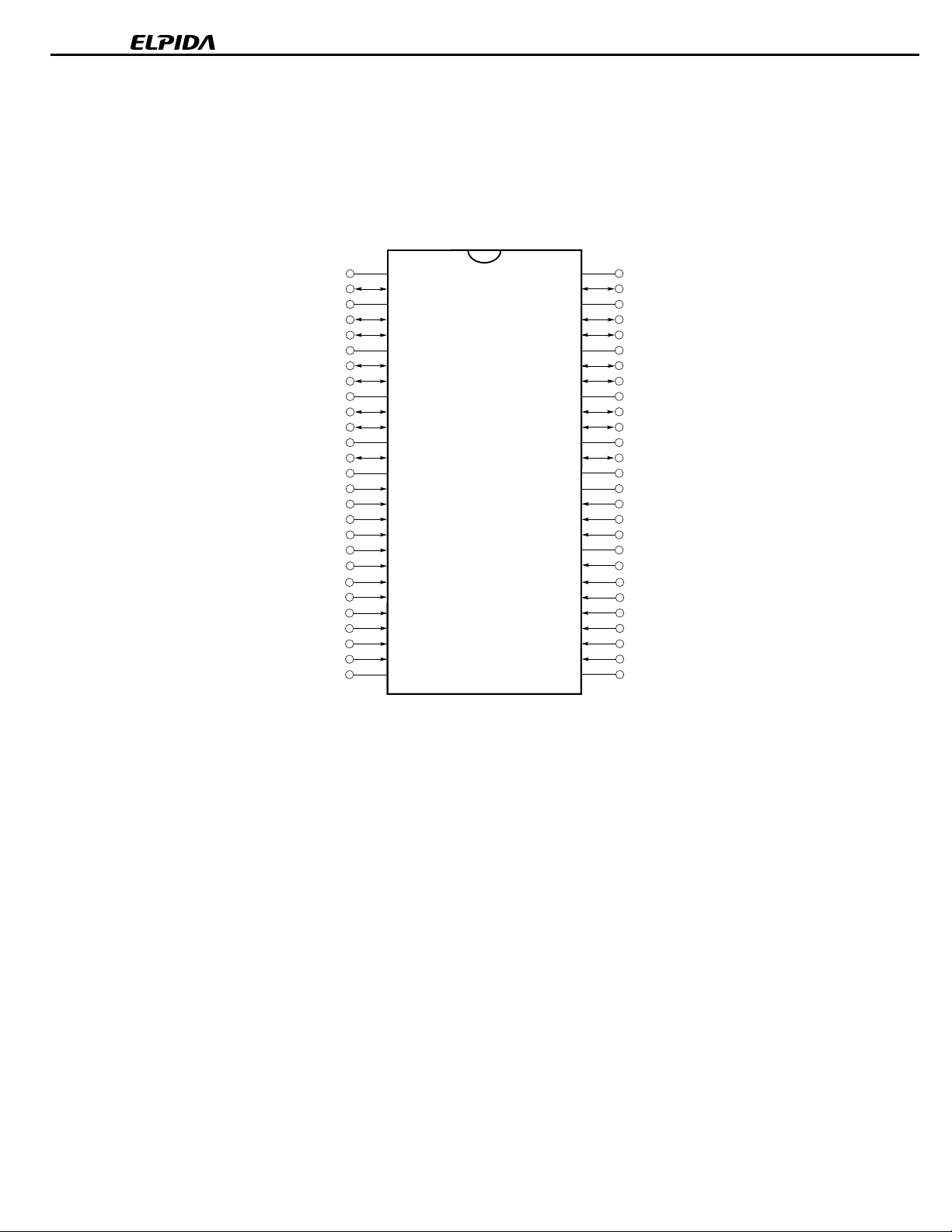
Pin Configurations
/xxx indicates active low signal.
BA0(A13)
BA1(A12)
PD45128163]
[
µµµµ
54-pin Plastic TSOP (II) (10.16mm (400))
2M words
16 bits
××××
V
DQ0
V
CC
DQ1
DQ2
SS
V
DQ3
DQ4
CC
V
DQ5
DQ6
V
SS
DQ7
V
LDQM
/WE
/CAS
/RAS
/CS
A10
A0
A1
A2
A3
V
CC
Q
Q
Q
Q
CC
CC
1
2
3
4
5
6
7
8
9
10
11
12
13
14
15
16
17
18
19
20
21
22
23
24
25
26
27
4 banks
××××
54
53
52
51
50
49
48
47
46
45
44
43
42
41
40
39
38
37
36
35
34
33
32
31
30
29
28
Vss
DQ15
VssQ
DQ14
DQ13
VccQ
DQ12
DQ11
VssQ
DQ10
DQ9
VccQ
DQ8
Vss
NC
UDQM
CLK
CKE
NC
A11
A9
A8
A7
A6
A5
A4
Vss
µµµµ
PD45128163-SU
Note
A0 to A11
: Address inputs
BA0(A13), BA1(A12) : Bank select
DQ0 to DQ15 : Data inputs / outputs
CLK : Clock input
CKE : Clock enable
/CS : Chip select
/RAS : Row address strobe
/CAS : Column address strobe
/WE : Write enable
LDQM : Lower DQ mask enable
UDQM : Upper DQ mask enable
CC
: Supply voltage
V
SS
: Ground
V
CC
Q : Supply voltage for DQ
V
SS
Q : Ground for DQ
V
Note
A0 to A11 : Row address inputs
A0 to A8 : Column address inputs
NC : No connection
4
Preliminary Data Sheet E0242N10
Page 5
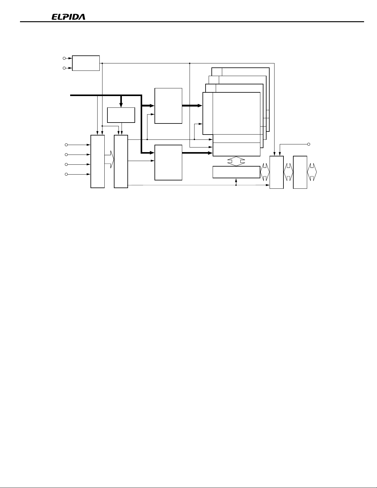
Block Diagram
CLK
CKE
Address
Clock
Generator
Mode
Register
Row
Address
Buffer
&
Refresh
Counter
Bank B
Bank A
Row Decoder
Bank D
Bank C
µµµµ
PD45128163-SU
/CS
/RAS
/CAS
/WE
Control Logic
Command Decoder
Column
Address
Buffer
&
Burst
Counter
Sense Amplifier
Column Decoder &
Latch Circuit
Data Control Circuit
Latch Circuit
DQM
DQ
Input & Output
Buffer
Preliminary Data Sheet E0242N10
5
Page 6

µµµµ
PD45128163-SU
CONTENTS
1. Input / Output Pin Function .............................................................................................................. 8
2. Commands ......................................................................................................................................... 9
3. Simplified State Diagram ................................................................................................................ 12
4. Truth Table ....................................................................................................................................... 13
4.1 Command Truth Table............................................................................................................................. 13
4.2 DQM Truth Table ...................................................................................................................................... 13
4.3 CKE Truth Table ....................................................................................................................................... 13
4.4 Operative Command Table ..................................................................................................................... 14
4.5 Command Truth Table for CKE .............................................................................................................. 17
5. Initialization ..................................................................................................................................... 18
6. Programming the Mode Register .................................................................................................. 19
7. Mode Register ................................................................................................................................. 20
7.1 Burst Length and Sequence ................................................................................................................... 21
8. Address Bits of Bank-Select and Precharge ................................................................................ 22
9. Precharge ......................................................................................................................................... 23
10. Auto Precharge ................................................................................................................................ 24
10.1 Read with Auto Precharge ................................................................................................................... 24
10.2 Write with Auto Precharge ................................................................................................................... 25
11. Read / Write Command Interval ..................................................................................................... 26
11.1 Read to Read Command Interval ........................................................................................................ 26
11.2 Write to Write Command Interval ........................................................................................................ 26
11.3 Write to Read Command Interval ........................................................................................................ 27
11.4 Read to Write Command Interval ........................................................................................................ 28
12. Burst Termination ........................................................................................................................... 29
12.1 Burst Stop Command ........................................................................................................................... 29
12.2 Precharge Termination ........................................................................................................................ 30
12.2.1 Precharge Termination in READ Cycle .................................................................................... 29
12.2.2 Precharge Termination in WRITE Cycle .................................................................................. 31
6
Preliminary Data Sheet E0242N10
Page 7

µµµµ
PD45128163-SU
13. Electrical Specifications ................................................................................................................. 32
13.1 AC Parameters for Read Timing .......................................................................................................... 37
13.2 AC Parameters for Write Timing ......................................................................................................... 39
13.3 Relationship between Frequency and Latency .................................................................................. 40
13.4 Mode Register Set ................................................................................................................................ 41
13.5 Power on Sequence and CBR (Auto) Refresh ................................................................................... 42
13.6 /CS Function ......................................................................................................................................... 43
13.7 Clock Suspension during Burst Read (using CKE Function) .......................................................... 44
13.8 Clock Suspension during Burst Write (using CKE Function) .......................................................... 46
13.9 Power Down Mode and Clock Mask ................................................................................................... 48
13.10 CBR (Auto) Refresh .............................................................................................................................. 49
13.11 Self Refresh (Entry and Exit) ............................................................................................................... 50
13.12 Random Column Read (Page with Same Bank) ................................................................................ 51
13.13 Random Column Write (Page with Same Bank) ................................................................................ 53
13.14 Random Row Read (Ping-Pong Banks) .............................................................................................. 55
13.15 Random Row Write (Ping-Pong Banks) ............................................................................................. 57
13.16 Read and Write ..................................................................................................................................... 59
13.17 Interleaved Column Read Cycle .......................................................................................................... 61
13.18 Interleaved Column Write Cycle .......................................................................................................... 63
13.19 Auto Precharge after Read Burst ........................................................................................................ 65
13.20 Auto Precharge after Write Burst ........................................................................................................ 67
13.21 Full Page Read Cycle ........................................................................................................................... 69
13.22 Full Page Write Cycle ........................................................................................................................... 71
13.23 Byte Write Operation ............................................................................................................................ 73
13.24 Burst Read and Single Write (Option) ................................................................................................ 75
13.25 Full Page Random Column Read ........................................................................................................ 77
13.26 Full Page Random Column Write ........................................................................................................ 79
13.27 PRE (Precharge) Termination of Burst ............................................................................................... 81
14. Package Drawing ............................................................................................................................ 83
15. Recommended Soldering Conditions ........................................................................................... 84
16. Revision History .............................................................................................................................. 85
Preliminary Data Sheet E0242N10
7
Page 8

µµµµ
PD45128163-SU
1. Input / Output Pin Function
Pin name Input / Output Function
CLK Input CLK is the master clock input. Other inputs signals are referenced to the CLK rising
edge.
CKE Input CKE determine validity of the next CLK (clock). If CKE is high, the next CLK rising edge
is valid; otherwise it is invalid. If the CLK rising edge is invalid, the internal clock is not
issued and the
When the
power down mode. During power down mode, CKE must remain low.
/CS Input /CS low starts the command input cycle. When /CS is high, commands are ignored but
operations continue.
/RAS, /CAS, /WE Input /RAS, /CAS and /WE have the same symbols on conventional DRAM but different
functions. For details, refer to the command table.
A0 - A11 Input
BA0, BA1 Input BA0(A13) and BA1(A12) are the bank select signal. In command cycle, BA0(A13) and
UDQM, LDQM Input
DQ0 - DQ15 Input / Output DQ pins have the same function as I/O pins on a conventional DRAM.
VCC, VSS, VCCQ, VSSQ (Power supply) VCC and VSS are power supply pins for internal circuits. VCCQ and VSSQ are power
Row Address is determined by A0 - A11 at the CLK (clock) rising edge in the active
command cycle.
Column Address is determined by A0
command cycle.
A10 defines the precharge mode. When A10 is high in the precharge command cycle,
all banks are precharged; when A10 is low, only the bank selected by BA0(A13) and
BA1(A12)
When A10 is high in read or write command cycle, the precharge starts automatically
after the burst access.
BA1(A12) low select bank A, BA0(A13) high and BA1(A12) low select bank B, BA0(A13)
low and BA1(A12) high select bank C and then BA0(A13) and BA1(A12) high select
bank D.
UDQM and LDQM control upper byte and lower byte I/O buffers, respectively.
In read mode, UDQM and LDQM controls the output buffers like a conventional /OE pin.
UDQM and LDQM high and UDQM and LDQM low turn the output buffers off and on,
respectively.
The UDQM and LDQM latency for the read is two clocks.
In write mode, UDQM and LDQM controls the word mask. Input data is written to the
memory cell if UDQM and LDQM is low but not if UDQM and LDQM is high.
The UDQM and LDQM latency for the write is zero.
supply pins for the output buffers.
µ
PD45128163 suspends operation.
µ
PD45128163 is not in burst mode and CKE is negated, the device enters
-
A8 at the CLK rising edge in the read or write
is precharged.
8
Preliminary Data Sheet E0242N10
Page 9
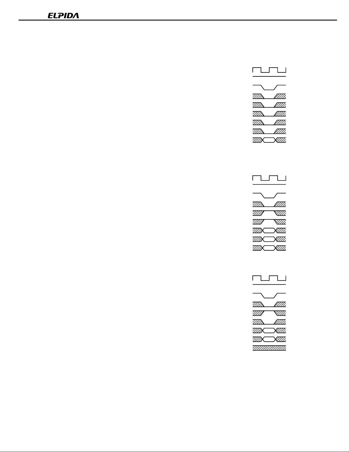
2. Commands
Mode register set command
(/CS, /RAS, /CAS, /WE = Low)
The µPD45128163 has a mode register that defines how the device
operates. In this command, A0 through A11, BA0(A13) and BA1(A12)
are the data input pins. After power on, the mode register set
command must be executed to initialize the device.
The mode register can be set only when all banks are in idle state.
RSC
During 2 CLK (t
cannot accept any other commands.
Activate command
(/CS, /RAS = Low, /CAS, /WE = High)
µ
The
PD45128163 has four banks, each with 4,096 rows.
This command activates the bank selected by BA0(A13) and
BA1(A12) and a row address selected by A0 through A11.
This command corresponds to a conventional DRAM’s /RAS falling.
Precharge command
(/CS, /RAS, /WE = Low, /CAS = High)
This command begins precharge operation of the bank selected by
BA0(A13) and BA1(A12). When A10 is High, all banks are
precharged, regardless of BA0(A13) and BA1(A12). When A10 is
Low, only the bank selected by BA0(A13) and BA1(A12) is
precharged.
After this command, the
command to the precharging bank during t
command period).
This command corresponds to a conventional DRAM’s /RAS rising.
) following this command, the µPD45128163
PD45128163 can’t accept the activate
µ
RP
(precharge to activate
µµµµ
PD45128163-SU
Fig.1 Mode register set command
CLK
CKE
H
/CS
/RAS
/CAS
/WE
BA0(A13), BA1(A12)
A10
Add
Fig.2 Row address strobe and
bank activate command
CLK
CKE
H
/CS
/RAS
/CAS
/WE
BA0(A13), BA1(A12)
A10
Add
Row
Row
Fig.3 Precharge command
CLK
CKE
H
/CS
/RAS
/CAS
/WE
BA0(A13), BA1(A12)
(Precharge select)
A10
Add
Preliminary Data Sheet E0242N10
9
Page 10
Write command
(/CS, /CAS, /WE = Low, /RAS = High)
If the mode register is in the burst write mode, this command sets the
burst start address given by the column address to begin the burst
write operation. The first write data in burst mode can input with this
command with subsequent data on following clocks.
Read command
(/CS, /CAS = Low, /RAS, /WE = High)
Read data is available after /CAS latency requirements have been
met. This command sets the burst start address given by the column
address.
CBR (auto) refresh command
(/CS, /RAS, /CAS = Low, /WE, CKE = High)
This command is a request to begin the CBR (auto) refresh
operation. The refresh address is generated internally.
Before executing CBR (auto) refresh, all banks must be precharged.
After this cycle, all banks will be in the idle (precharged) state and
ready for a row activate command.
RC
During t
command), the
period (from refresh command to refresh or activate
PD45128163 cannot accept any other command.
µ
µµµµ
PD45128163-SU
Fig.4 Column address and write command
CLK
CKE
H
/CS
/RAS
/CAS
/WE
BA0(A13), BA1(A12)
A10
Add
Col.
Fig.5 Column address and read command
CLK
CKE
H
/CS
/RAS
/CAS
/WE
BA0(A13), BA1(A12)
A10
Add
Col.
Fig.6 CBR (auto) refresh command
CLK
CKE
H
/CS
/RAS
/CAS
/WE
BA0(A13), BA1(A12)
A10
Add
10
Preliminary Data Sheet E0242N10
Page 11
Self refresh entry command
(/CS, /RAS, /CAS, CKE = Low, /WE = High)
After the command execution, self refresh operation continues while
µ
CKE remains low. When CKE goes high, the
PD45128163 exits the
self refresh mode.
During self refresh mode, refresh interval and refresh operation are
performed internally, so there is no need for external control.
Before executing self refresh, all banks must be precharged.
Burst stop command
(/CS, /WE = Low, /RAS, /CAS = High)
This command can stop the current burst operation.
No operation
(/CS = Low, /RAS, /CAS, /WE = High)
This command is not an execution command. No operations begin
or terminate by this command.
µµµµ
PD45128163-SU
Fig.7 Self refresh entry command
CLK
CKE
/CS
/RAS
/CAS
/WE
BA0(A13), BA1(A12)
A10
Add
Fig.8 Burst stop command in Full Page
Mode
CLK
CKE
H
/CS
/RAS
/CAS
/WE
BA0(A13), BA1(A12)
A10
Add
Fig.9 No operation
CLK
CKE
H
/CS
/RAS
/CAS
/WE
BA0(A13), BA1(A12)
A10
Add
Preliminary Data Sheet E0242N10
11
Page 12
3. Simplified State Diagram
SELF
Self
Refresh
µµµµ
PD45128163-SU
WRITE
SUSPEND
CKE
Mode
Register
Set
Write
CKE
WRITE
BST
MRS
Write
IDLE
ROW
ACTIVE
Write with
Read
Auto precharge
ACT
Auto precharge
PRE
Write
Read
Read with
SELF exit
REF
CKE
CKE
CKE
CKE
BST
READ
CBR (Auto)
Refresh
Power
Down
Active
Power
Down
Read
CKE
CKE
READ
SUSPEND
WRITEA
SUSPEND
12
POWER
ON
CKE
CKE
WRITEA
Precharge
PRE (Precharge termination)
PRE (Precharge termination)
Precharge
Preliminary Data Sheet E0242N10
READA
CKE
CKE
READA
SUSPEND
Automatic sequence
Manual input
Page 13
µµµµ
PD45128163-SU
4. Truth Table
4.1 Command Truth Table
Function Symbol CKE /CS /RAS /CAS /WE BA1, A10 A11,
n – 1 n BA0 A9 - A0
Device deselect DESL H × H × × × × × ×
No operation NOP H × L H H H × × ×
Burst stop BST H × L H H L × × ×
Read READ H × L H L H V L V
Read with auto precharge READA H × L H L H V H V
Write WRIT H × L H L L V L V
Write with auto precharge WRITA H × L H L L V H V
Bank activate ACT H × L L H H V V V
Precharge select bank PRE H
Precharge all banks PALL H
Mode register set MRS H
L L H L V L ×
×
L L H L × H ×
×
L L L L L L V
×
Remark
H = High level, L = Low level, × = High or Low level (Don't care), V = Valid data input
4.2 DQM Truth Table
Function Symbol CKE DQM
n – 1 n U L
Data write / output enable ENB H × L
Data mask / output disable MASK H × H
Upper byte write enable / output enable ENBU H × L ×
Lower byte write enable / output enable ENBL H × × L
Upper byte write inhibit / output disable MASKU H × H ×
Lower byte write inhibit / output disable MASKL H × × H
Remark
H = High level, L = Low level, × = High or Low level (Don't care)
4.3 CKE Truth Table
Current state Function Symbol CKE /CS /RAS /CAS /WE Address
n – 1 n
Activating Clock suspend mode entry H L
Any Clock suspend mode L L × × × × ×
Clock suspend Clock suspend mode exit L H × × × × ×
Idle CBR (auto) refresh command REF H H L L L H ×
Idle Self refresh entry SELF H L L L L H ×
Self refresh Self refresh exit L H L H H H ×
L H H × × × ×
Idle Power down entry H L × × × × ×
Power down Power down exit L H H × × × ×
L H L H H H ×
×
×
×
×
×
Remark
H = High level, L = Low level, × = High or Low level (Don't care)
Preliminary Data Sheet E0242N10
13
Page 14
µµµµ
PD45128163-SU
4.4 Operative Command Table
Current state /CS /RAS /CAS /WE Address Command Action Notes
Idle H × × × × DESL Nop or power down 2
L H H × × NOP or BST Nop or power down 2
L H L H BA, CA, A10 READ/READA ILLEGAL 3
L H L L BA, CA, A10 WRIT/WRITA ILLEGAL 3
L L H H BA, RA ACT Row activating
L L H L BA, A10 PRE/PALL Nop
L L L H × REF/SELF CBR (auto) refresh or self refresh 4
L L L L Op-Code MRS Mode register accessing
Row active H ×
L H H × × NOP or BST Nop
L H L H BA, CA, A10 READ/READA Begin read : Determine AP 5
L H L L BA, CA, A10 WRIT/WRITA Begin write : Determine AP 5
L L H H BA, RA ACT ILLEGAL 3
L L H L BA, A10 PRE/PALL Precharge 6
L L L H × REF/SELF ILLEGAL
L L L L Op-Code MRS ILLEGAL
Read H
L H H H × NOP Continue burst to end → Row active
L H H L
L H L H BA, CA, A10 READ/READA Terminate burst, new read : Determine AP 7
L H L L BA, CA, A10 WRIT/WRITA Terminate burst, start write : Determine AP 7, 8
L L H H BA, RA ACT ILLEGAL 3
L L H L BA, A10 PRE/PALL Terminate burst, precharging
L L L H × REF/SELF ILLEGAL
L L L L Op-Code MRS ILLEGAL
Write H × × × × DESL Continue burst to end → Write recovering
L H H H
L H H L × BST Burst stop → Row active
L H L H BA, CA, A10 READ/READA Terminate burst, start read : Determine AP 7, 8
L H L L BA, CA, A10 WRIT/WRITA Terminate burst, new write : Determine AP 7
L L H H BA, RA ACT ILLEGAL 3
L L H L BA, A10 PRE/PALL Terminate burst, precharging 9
L L L H × REF/SELF ILLEGAL
L L L L Op-Code MRS ILLEGAL
× × × ×
Note1
× × ×
(1/3)
DESL Nop
DESL Continue burst to end → Row active
BST Burst stop
×
NOP Continue burst to end → Write recovering
×
Row active
→
14
Preliminary Data Sheet E0242N10
Page 15
µµµµ
PD45128163-SU
(2/3)
Current state /CS /RAS /CAS /WE Address Command Action Notes
Read with auto H × × × × DESL Continue burst to end → Precharging
precharge L H H H × NOP Continue burst to end → Precharging
L H H L
L H L H BA, CA, A10 READ/READA ILLEGAL 3
L H L L BA, CA, A10 WRIT/WRITA ILLEGAL 3
L L H H BA, RA ACT ILLEGAL 3
L L H L BA, A10 PRE/PALL ILLEGAL 3
L L L H × REF/SELF ILLEGAL
L L L L Op-Code MRS ILLEGAL
Write with auto
precharge
L H H L × BST ILLEGAL
L H L H BA, CA, A10 READ/READA ILLEGAL 3
L H L L BA, CA, A10 WRIT/WRITA ILLEGAL 3
L L H H BA, RA ACT ILLEGAL 3
L L H L BA, A10 PRE/PALL ILLEGAL 3
L L L H × REF/SELF ILLEGAL
L L L L Op-Code MRS ILLEGAL
Precharging H
L H H H × NOP Nop → Enter idle after t
L H H L
L H L H BA, CA, A10 READ/READA ILLEGAL 3
L H L L BA, CA, A10 WRIT/WRITA ILLEGAL 3
L L H H BA, RA ACT ILLEGAL 3
L L H L BA, A10 PRE/PALL Nop → Enter idle after tRP
L L L H × REF/SELF ILLEGAL
L L L L Op-Code MRS ILLEGAL
Row activating H × × × × DESL Nop → Enter bank active after t
L H H H
L H H L × BST ILLEGAL
L H L H BA, CA, A10 READ/READA ILLEGAL 3
L H L L BA, CA, A10 WRIT/WRITA ILLEGAL 3
L L H H BA, RA ACT ILLEGAL 3, 10
L L H L BA, A10 PRE/PALL ILLEGAL 3
L L L H × REF/SELF ILLEGAL
L L L L Op-Code MRS ILLEGAL
H
×
×
L H H H
× × × ×
BST ILLEGAL
×
×
×
×
DESL Nop
BST ILLEGAL
×
NOP Nop
×
DESL
NOP
Continue burst to end → Write
recovering with auto precharge
Continue burst to end → Write
recovering with auto precharge
Enter idle after tRP
→
RP
RCD
Enter bank active after t
→
RCD
Preliminary Data Sheet E0242N10
15
Page 16
µµµµ
PD45128163-SU
(3/3)
Current state /CS /RAS /CAS /WE Address Command Action Notes
Write recovering H × × × × DESL Nop → Enter row active after t
L H H H × NOP Nop → Enter row active after t
L H H L
L H L H BA, CA, A10 READ/READA Start read, Determine AP 8
L H L L BA, CA, A10 WRIT/WRITA New write, Determine AP
L L H H BA, RA ACT ILLEGAL 3
L L H L BA, A10 PRE/PALL ILLEGAL 3
L L L H × REF/SELF ILLEGAL
L L L L Op-Code MRS ILLEGAL
Write recovering H × × × × DESL Nop → Enter precharge after t
with auto precharge L H H H × NOP Nop
L H H L × BST Nop → Enter precharge after t
L H L H BA, CA, A10 READ/READA ILLEGAL 3, 8
L H L L BA, CA, A10 WRIT/WRITA ILLEGAL 3
L L H H BA, RA ACT ILLEGAL 3
L L H L BA, A10 PRE/PALL ILLEGAL
L L L H × REF/SELF ILLEGAL
L L L L Op-Code MRS ILLEGAL
Refreshing H
L H H × × NOP/BST Nop → Enter idle after t
L H L
L L H × ×
L L L × ×
Mode register H × × × × DESL Nop → Enter idle after t
accessing L H H H
L H H L × BST ILLEGAL
L H L
× × × ×
L L
×
BST Nop
×
DESL Nop
READ/WRIT ILLEGAL
× ×
ACT/PRE/PALL
REF/SELF/MRS
NOP Nop
×
READ/WRIT ILLEGAL
× ×
×
×
ACT/PRE/PALL/
REF/SELF/MRS
Enter row active after t
→
Enter precharge after t
→
Enter idle after tRC
→
ILLEGAL
ILLEGAL
Enter idle after t
→
ILLEGAL
DPL
DPL
DPL
DPL
DPL
DPL
RC
RSC
RSC
Notes 1.
Remark
16
All entries assume that CKE was active (High level) during the preceding clock cycle.
2.
If all banks are idle, and CKE is inactive (Low level),
µ
PD45128163 will enter Power down mode.
All input buffers except CKE will be disabled.
3.
Illegal to bank in specified states; Function may be legal in the bank indicated by Bank Address (BA),
depending on the state of that bank.
4.
If all banks are idle, and CKE is inactive (Low level),
µ
PD45128163 will enter Self refresh mode. All input
buffers except CKE will be disabled.
5.
Illegal if t
6.
Illegal if t
7.
Must satisfy burst interrupt condition.
8.
Must satisfy bus contention, bus turn around, and/or write recovery requirements.
9.
Must mask preceding data which don't satisfy t
10.
Illegal if t
RCD
is not satisfied.
RAS
is not satisfied.
RRD
is not satisfied.
DPL
.
H = High level, L = Low level, × = High or Low level (Don’t care), V = Valid data
Preliminary Data Sheet E0242N10
Page 17
µµµµ
PD45128163-SU
4.5 Command Truth Table for CKE
Current State CKE /CS /RAS /CAS /WE Address Action Notes
n – 1 n
Self refresh H × × × × × × INVALID, CLK (n – 1) would exit self refresh
L H H × × × × Self refresh recovery
L H L H H × × Self refresh recovery
L H L H L × × ILLEGAL
L H L L × × × ILLEGAL
L L
Self refresh recovery H H H × × × × Idle after t
H H L H H × × Idle after tRC
H H L H L × × ILLEGAL
H H L L × × × ILLEGAL
H L H
H L L H H × × ILLEGAL
H L L H L × × ILLEGAL
H L L L × × × ILLEGAL
Power down H × × × × × INVALID, CLK (n – 1) would exit power down
L H H
L H L H H H × EXIT power down → Idle
L L × × × × × Maintain power down mode
All banks idle H H H × × × Refer to operations in Operative Command Table
H H L H × × Refer to operations in Operative Command Table
H H L L H × Refer to operations in Operative Command Table
H H L L L H × CBR (auto) Refresh
H H L L L L Op-Code Refer to operations in Operative Command Table
H L H
H L L H × × Refer to operations in Operative Command Table
H L L L H × Refer to operations in Operative Command Table
H L L L L H × Self refresh 1
H L L L L L Op-Code Refer to operations in Operative Command Table
L
Row active H × × × × × × Refer to operations in Operative Command Table
L × × × × × × Power down 1
Any state other than H H × × × × Refer to operations in Operative Command Table
listed above H L × × × × × Begin clock suspend next cycle 2
L H
L L
× × × × ×
× × × ×
× × × ×
× × ×
× × × × × ×
× × × × ×
× × × × ×
Maintain self refresh
RC
ILLEGAL
EXIT power down → Idle
Refer to operations in Operative Command Table
Power down 1
Exit clock suspend next cycle
Maintain clock suspend
Notes 1.
Self refresh can be entered only from the all banks idle state. Power down can be entered only from all
banks idle or row active state.
2.
Must be legal command as defined in Operative Command Table.
Remark
H = High level, L = Low level, × = High or Low level (Don't care)
Preliminary Data Sheet E0242N10
17
Page 18

µµµµ
PD45128163-SU
5. Initialization
The synchronous DRAM is initialized in the power-on sequence according to the following.
µ
(1) To stabilize internal circuits, when power is applied, a 100
(2) After the pause, all banks must be precharged using the Precharge command (The Precharge all banks
command is convenient).
(3) Once the precharge is completed and the minimum t
RSC
After the mode register set cycle, t
(4) Two or more CBR (Auto) refresh must be performed.
Remarks 1.
The sequence of Mode register programming and Refresh above may be transposed.
2.
CKE and DQM must be held high until the Precharge command is issued to ensure data-bus Hi-Z.
(2 CLK minimum) pause must be satisfied as well.
s or longer pause must precede any signal toggling.
RP
is satisfied, the mode register can be programmed.
18
Preliminary Data Sheet E0242N10
Page 19

µµµµ
PD45128163-SU
6. Programming the Mode Register
The mode register is programmed by the Mode register set command using address bits A11 through A0, BA0(A13)
and BA1(A12) as data inputs. The register retains data until it is reprogrammed or the device loses power.
The mode register has four fields;
Options : A11 through A7, BA0(A13), BA1(A12)
/CAS latency : A6 through A4
Wrap type : A3
Burst length : A2 through A0
Following mode register programming, no command can be issued before at least 2 CLK have elapsed.
/CAS Latency
/CAS latency is the most critical of the parameters being set. It tells the device how many clocks must elapse
before the data will be available.
The value is determined by the frequency of the clock and the speed grade of the device.
between Frequency and Latency
the device.
Burst Length
Burst Length is the number of words that will be output or input in a read or write cycle. After a read burst is
completed, the output bus will become Hi-Z.
The burst length is programmable as 1, 2, 4, 8 or full page.
Wrap Type (Burst Sequence)
The wrap type specifies the order in which the burst data will be addressed. This order is programmable as either
“Sequential” or “Interleave”. The method chosen will depend on the type of CPU in the system.
Some microprocessor cache systems are optimized for sequential addressing and others for interleaved addressing.
7.1 Burst Length and Sequence
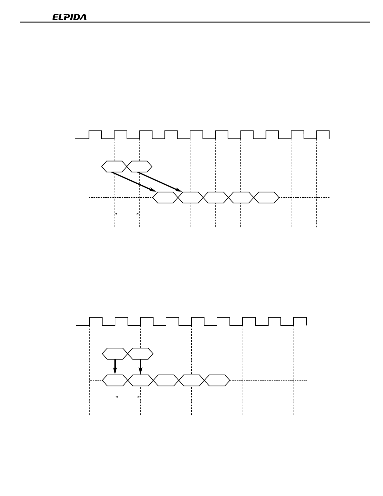
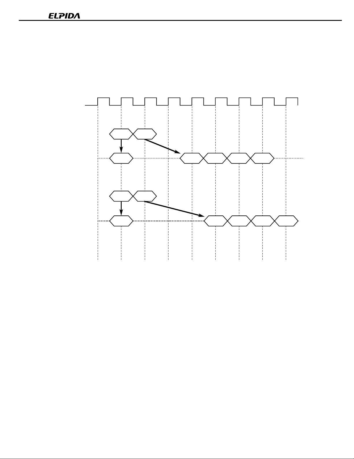
sequences support bursts of 1, 2, 4 and 8. Additionally, sequence supports the full page length.
shows the relationship of /CAS latency to the clock period and the speed grade of
shows the addressing sequence for each burst length using them. Both
13.3 Relationship
Preliminary Data Sheet E0242N10
19
Page 20
7. Mode Register
BA1
BA0
(A12)
(A13)
00
BA1
BA0
(A12)
(A13)
xx
BA1
BA0
(A12)
(A13)
BA1
BA0
(A12)
(A13)
xx
BA1
BA0
(A12)
(A13)
00
µµµµ
PD45128163-SU
A0A1A2A3A4A5A7 A6A8A9A10A11
10000 JEDEC Standard Test Set (refresh counter test)
A0A1A2A3A4A5A7 A6A8A9A10A11
BLWTLTMODE001xx Burst Read and Single Write
01 Use in future
BLWTLTMODE00000 Mode Register Set
(for Write Through Cache)
A0A1A2A3A4A5A7 A6A8A9A10A11
A0A1A2A3A4A5A7 A6A8A9A10A11
VVVVVV1V1xxx Vender Specific
A0A1A2A3A4A5A7 A6A8A9A10A11
V = Valid
x = Don’t care
Burst length
Wrap type
Latency
Remark R : Reserved
Mode Register Set Timing
mode
Bits2-0
000
001
010
011
100
101
110
111
0
1
Full page
Sequential
Interleave
Bits6-4
000
001
010
011
100
101
110
111
WT = 0
1
2
4
8
R
R
R
/CAS latency
WT = 1
1
2
4
8
R
R
R
R
R
R
2
3
R
R
R
R
20
CLK
CKE
/CS
/RAS
/CAS
/WE
A0 - A11,
BA0(13), BA1(A12)
Preliminary Data Sheet E0242N10
Mode Register Set
Page 21
7.1 Burst Length and Sequence
[Burst of Two]
Starting address
(column address A0, binary)
0 0, 1 0, 1
1 1, 0 1, 0
[Burst of Four]
Starting address
(column address A1 - A0, binary)
00 0, 1, 2, 3 0, 1, 2, 3
01 1, 2, 3, 0 1, 0, 3, 2
10 2, 3, 0, 1 2, 3, 0, 1
11 3, 0, 1, 2 3, 2, 1, 0
[Burst of Eight]
Starting address
(column address A2 - A0, binary)
000 0, 1, 2, 3, 4, 5, 6, 7 0, 1, 2, 3, 4, 5, 6, 7
001 1, 2, 3, 4, 5, 6, 7, 0 1, 0, 3, 2, 5, 4, 7, 6
010 2, 3, 4, 5, 6, 7, 0, 1 2, 3, 0, 1, 6, 7, 4, 5
011 3, 4, 5, 6, 7, 0, 1, 2 3, 2, 1, 0, 7, 6, 5, 4
100 4, 5, 6, 7, 0, 1, 2, 3 4, 5, 6, 7, 0, 1, 2, 3
101 5, 6, 7, 0, 1, 2, 3, 4 5, 4, 7, 6, 1, 0, 3, 2
110 6, 7, 0, 1, 2, 3, 4, 5 6, 7, 4, 5, 2, 3, 0, 1
111 7, 0, 1, 2, 3, 4, 5, 6 7, 6, 5, 4, 3, 2, 1, 0
Sequential addressing sequence
(decimal)
Sequential addressing sequence
(decimal)
Sequential addressing sequence
(decimal)
µµµµ
PD45128163-SU
Interleave addressing sequence
(decimal)
Interleave addressing sequence
(decimal)
Interleave addressing sequence
(decimal)
Full page burst is an extension of the above tables of sequential addressing, with the length being 512.
Preliminary Data Sheet E0242N10
21
Page 22

8. Address Bits of Bank-Select and Precharge
(Activate command)
(Precharge command)
(/CAS strobes)
µµµµ
PD45128163-SU
BA1
(A12)
BA1
(A12)
BA1
(A12)
BA0
(A13)
BA0
(A13)
BA0
(A13)
A11A10A9A8A7A6A4 A5A3A2A1A0Row
A11A10A9A8A7A6A4 A5A3A2A1A0
xA10A9A8A7A6A4 A5A3A2A1A0Col.
BA1(A12) BA0(A13)
0
0
0
1
1
0
1
1
BA1(A12) BA0(A13)
A10
0
0
0
0
0
1
0
1
1
x
x : Don’t care
disables Auto-Precharge
0
(End of Burst)
enables Auto-Precharge
1
(End of Burst)
Result
Select Bank A
“Activate” command
Select Bank B
“Activate” command
Select Bank C
“Activate” command
Select Bank D
“Activate” command
Result
Precharge Bank A
0
Precharge Bank B
1
Precharge Bank C
0
Precharge Bank D
1
Precharge All Banks
x
BA1(A12) BA0(A13)
0
0
0
1
1
0
1
1
Result
enables Read/Write
commands for Bank A
enables Read/Write
commands for Bank B
enables Read/Write
commands for Bank C
enables Read/Write
commands for Bank D
22
Preliminary Data Sheet E0242N10
Page 23
µµµµ
PD45128163-SU
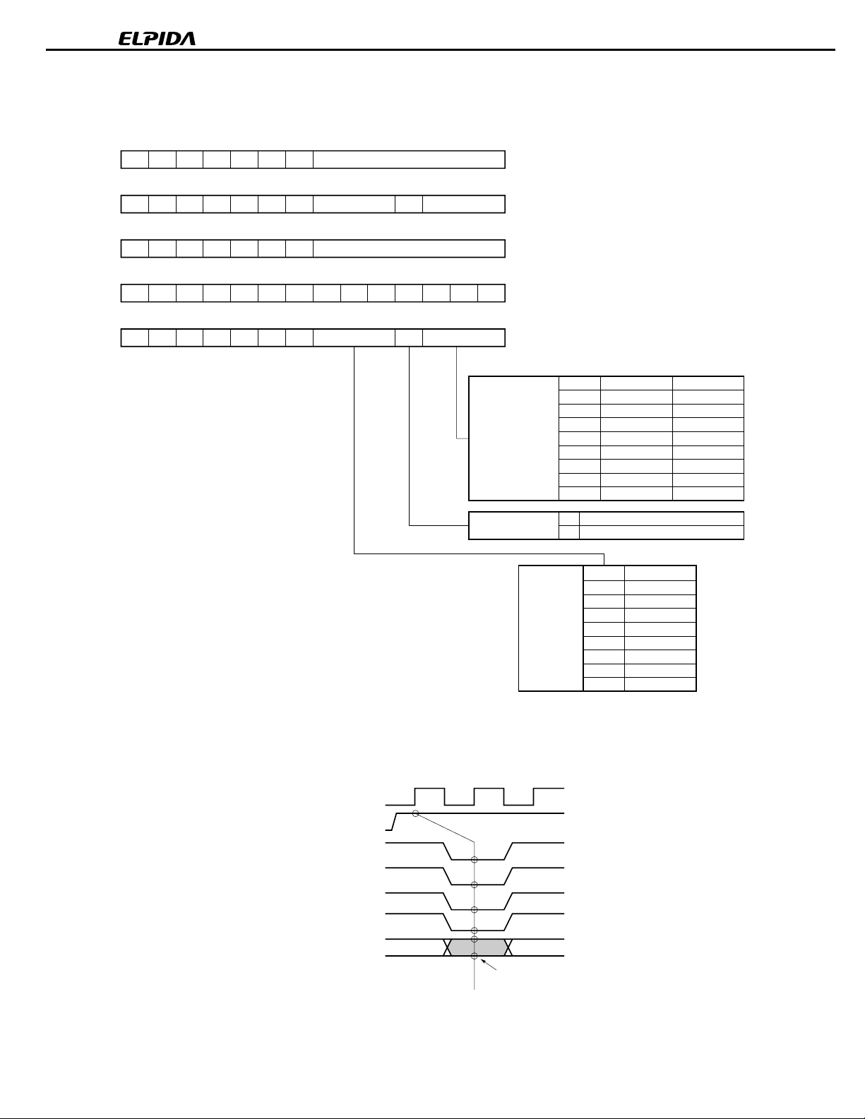
9. Precharge
RAS (MIN.)
The precharge command can be issued anytime after t
Soon after the precharge command is issued, precharge operation performed and the synchronous DRAM enters
RP
the idle state after t
is satisfied. The parameter tRP is the time required to perform the precharge.
The earliest timing in a read cycle that a precharge command can be issued without losing any data in the burst is
as follows.
It is depending on the /CAS latency and clock cycle time.
T0 T1 T2 T3 T4 T5 T6 T7
CLK
/CAS latency = 2
Command
READ
is satisfied.
Burst length=4
T8
PRE
Hi-Z
Hi-Z
/CAS latency = 3
Command
DQ
DQ
READ
Q1 Q2 Q3 Q4
PRE
Q1 Q2 Q3 Q4
(t
RAS
must be satisfied)
DPL
In order to write all data to the memory cell correctly, the asynchronous parameter “t
(MIN.)
specification defines the earliest time that a precharge command can be issued. Minimum number of clocks is
DPL (MIN.)
calculated by dividing t
with clock cycle time.
” must be satisfied. The t
In summary, the precharge command can be issued relative to reference clock that indicates the last data word is
valid. In the following table, minus means clocks before the reference; plus means time after the reference.
/CAS latency Read Write
2 –1 +t
3 –2 +t
DPL (MIN.)
DPL (MIN.)
DPL
Preliminary Data Sheet E0242N10
23
Page 24
µµµµ
PD45128163-SU
10. Auto Precharge
During a read or write command cycle, A10 controls whether auto precharge is selected. A10 high in the Read or
Write command (Read with Auto precharge command or Write with Auto precharge command), auto precharge is
selected and begins automatically.
RAS
The t
next activate command to the bank being precharged cannot be executed until the precharge cycle ends.
In read cycle, once auto precharge has started, an activate command to the bank can be issued after t
satisfied.
In write cycle, the t
The timing that begins the auto precharge cycle depends on both the /CAS latency programmed into the mode
register and whether read or write cycle.
10.1 Read with Auto Precharge
During a read cycle, the auto precharge begins one clock earlier (/CAS latency of 2) or two clocks earlier (/CAS
latency of 3) the last data word output.
must be satisfied with a read with auto precharge or a write with auto precharge operation. In addition, the
RP
has been
DAL
must be satisfied to issue the next activate command to the bank being precharged.
Burst length = 4
T0 T2T1 T3 T4 T5 T6 T7 T8
CLK
T9
/CAS latency = 2
Command
DQ
/CAS latency = 3
Command
DQ
Remark
READA means Read with Auto precharge
READA B
READA B
Auto precharge starts
QB1 QB2 QB3 QB4
Auto precharge starts
QB1 QB2 QB3 QB4
Hi-Z
(t
RAS
must be satisfied)
Hi-Z
24
Preliminary Data Sheet E0242N10
Page 25
10.2 Write with Auto Precharge
During a write cycle, the auto precharge starts at the timing that is equal to the value of the t
data word input to the device.
T0 T2T1 T3 T4 T5 T6 T7 T8
CLK
µµµµ
PD45128163-SU
DPL (MIN.)
after the last
Burst length = 4
/CAS latency = 2
Command
DQ
/CAS latency = 3
Command
DQ
WRITA B
DB1 DB2 DB3 DB4
WRITA B
DB1 DB2 DB3 DB4
Auto precharge starts
t
DPL(MIN.)
Auto precharge starts
t
DPL(MIN.)
Hi-Z
Hi-Z
RAS
must be satisfied)
(t
Remark
WRITA means Write with Auto Precharge
In summary, the auto precharge begins relative to a reference clock that indicates the last data word is valid.
In the table below, minus means clocks before the reference; plus means after the reference.
/CAS latency Read Write
2 –1 +t
3 –2 +t
DPL (MIN.)
DPL (MIN.)
Preliminary Data Sheet E0242N10
25
Page 26
µµµµ
PD45128163-SU
11. Read / Write Command Interval
11.1 Read to Read Command Interval
During a read cycle, when new Read command is issued, it will be effective after /CAS latency, even if the previous
read operation does not completed. READ will be interrupted by another READ.
The interval between the commands is 1 cycle minimum. Each Read command can be issued in every clock
without any restriction.
T0 T2T1 T3 T4 T5 T6 T7 T8
CLK
Burst length = 4, /CAS latency = 2
T9
Command
DQ
READ A
1cycle
READ B
QA1
QB1 QB2 QB3 QB4
Hi-Z
11.2 Write to Write Command Interval
During a write cycle, when a new Write command is issued, the previous burst will terminate and the new burst will
begin with a new Write command. WRITE will be interrupted by another WRITE.
The interval between the commands is minimum 1 cycle. Each Write command can be issued in every clock
without any restriction.
Burst length = 4, /CAS latency = 2
T0 T2T1 T3 T4 T5 T6 T7 T8
CLK
Command
DQ
26
WRITE A
DA1
WRITE B
DB1 DB2 DB3 DB4
1cycle
Preliminary Data Sheet E0242N10
Hi-Z
Page 27
11.3 Write to Read Command Interval
Write command and Read command interval is also 1 cycle.
Only the write data before Read command will be written.
The data bus must be Hi-Z at least one cycle prior to the first D
T0 T2T1 T3 T4 T5 T6 T7 T8
CLK
/CAS latency = 2
Command
WRITE A
READ B
OUT
µµµµ
PD45128163-SU
.
Burst length = 4
DQ
/CAS latency = 3
Command
DQ
DA1
WRITE A
DA1
READ B
Hi-Z
Hi-Z
QB1 QB2 QB3 QB4
QB1 QB2 QB3 QB4
Preliminary Data Sheet E0242N10
27
Page 28

µµµµ
PD45128163-SU
11.4 Read to Write Command Interval
During a read cycle, READ can be interrupted by WRITE.
The Read and Write command interval is 1 cycle minimum. There is a restriction to avoid data conflict. The Data
bus must be Hi-Z using DQM before WRITE.
Burst length = 4
T0 T2T1 T3 T4 T5 T6 T7 T8
CLK
Command
DQM
DQ
READ
Hi-Z
WRITE
D1 D2 D3 D4
1cycle
READ can be interrupted by WRITE. DQM must be High at least 3 clocks prior to the Write command.
Burst length = 8
T9
CLK
/CAS latency = 2
Command
DQM
DQ
/CAS latency = 3
Command
T0 T2T1 T3 T4 T5 T6 T7 T8
READ
READ
Q1 Q2 Q3
Hi-Z is
necessary
WRITE
D1 D2 D3
WRITE
28
DQM
DQ
Q1 Q2
Preliminary Data Sheet E0242N10
Hi-Z is
necessary
D1 D2 D3
Page 29

µµµµ
PD45128163-SU
12. Burst Termination
There are two methods to terminate a burst operation other than using a Read or a Write command. One is the
burst stop command and the other is the precharge command.
12.1 Burst Stop Command
During a read cycle, when the burst stop command is issued, the burst read data are terminated and the data bus
goes to Hi-Z after the /CAS latency from the burst stop command.
T0 T2T1 T3 T4 T5 T6 T7
CLK
Burst length = X
READCommand
/CAS latency = 2
Q1 Q2 Q3DQ
/CAS latency = 3
BST
Q1 Q2 Q3DQ
Hi-Z
Hi-Z
Remark
BST: Burst stop command
During a write cycle, when the burst stop command is issued, the burst write data are terminated and data bus goes
to Hi-Z at the same clock with the burst stop command.
Burst length = X
T0 T2T1 T3 T4 T5 T6 T7
CLK
Command
/CAS latency = 2, 3
DQ
WRITE
D1
D2 D3 D4
BST
Hi-Z
Remark
BST: Burst stop command
Preliminary Data Sheet E0242N10
29
Page 30

µµµµ
PD45128163-SU
12.2 Precharge Termination
12.2.1 Precharge Termination in READ Cycle
During a read cycle, the burst read operation is terminated by a precharge command.
When the precharge command is issued, the burst read operation is terminated and precharge starts.
RP
The same bank can be activated again after t
RAS
To issue a precharge command, t
must be satisfied.
from the precharge command.
When /CAS latency is 2, the read data will remain valid until one clock after the precharge command.
Burst length = X, /CAS latency = 2
T0 T2T1 T3 T4 T5 T6 T7
CLK
Command
READ
PRE
Q1DQ
Q2 Q3 Q4
t
(t
ACT
RP
RAS
must be satisfied)
Hi-Z
When /CAS latency is 3, the read data will remain valid until two clocks after the precharge command.
Burst length = X, /CAS latency = 3
CLK
Command
DQ
T0 T2T1 T3 T4 T5 T6 T7
READ
Q1 Q2 Q3
PRE
Q4
t
RP
(t
RAS
T8
ACT
Hi-Z
must be satisfied)
30
Preliminary Data Sheet E0242N10
Page 31

µµµµ
PD45128163-SU
12.2.2 Precharge Termination in WRITE Cycle
During a write cycle, the burst write operation is terminated by a precharge command.
When the precharge command is issued, the burst write operation is terminated and precharge starts.
RP
The same bank can be activated again after t
RAS
To issue a precharge command, t
must be satisfied.
from the precharge command.
When /CAS latency is 2, the write data written prior to the precharge command will be correctly stored. However,
invalid data may be written at the same clock as the precharge command. To prevent this from happening, DQM
must be high at the same clock as the precharge command. This will mask the invalid data.
Burst length = X, /CAS latency = 2
T0 T2T1 T3 T4 T5 T6 T7
CLK
Command
DQM
DQ
WRITE
D1 D2 D3
PRE
D4 D5
t
(t
RAS
ACT
Hi-Z
RP
must be satisfied)
When /CAS latency is 3, the write data written prior to the precharge command will be correctly stored. However,
invalid data may be written at the same clock as the precharge command. To prevent this from happening, DQM
must be high at the same clock as the precharge command. This will mask the invalid data.
Burst length = X, /CAS latency = 3
T8
ACT
CLK
Command
DQM
DQ
T0 T2T1 T3 T4 T5 T6 T7
WRITE
D1 D2 D3
D4
PRE
D5
Hi-Z
Preliminary Data Sheet E0242N10
t
RP
(t
RAS
must be satisfied)
31
Page 32

µµµµ
PD45128163-SU
13. Electrical Specifications
SS
All voltages are referenced to V
•
• After power up, wait more than 100
proper device operation is achieved.
Absolute Maximum Ratings
Parameter Symbol Condition Rating Unit
Voltage on power supply pin relative to GND VCC, V
Voltage on any pin relative to GND V
Short circuit output current IO 50 mA
Power dissipation PD 1 W
Operating ambient temperature T
Storage temperature T
Caution Exposing the device to stress above those listed in Absolute Maximum Ratings could cause
permanent damage. The device is not meant to be operated under conditions outside the limits
described in the operational section of this specification. Exposure to Absolute Maximum
Rating conditions for extended periods may affect device reliability.
Recommended Operating Conditions
Parameter Symbol Condition MIN. TYP. MAX. Unit
Supply voltage VCC, VCCQ 3.0 3.3 3.6 V
High level input voltage VIH 2.0 VCC+0.3
Low level input voltage V
Operating ambient temperature T
(GND).
µ
s and then, execute
CC
Q −0.5 to +4.6 V
T
−0.5 to +4.6 V
A
−20 to + 70 °C
stg
IL
−0.3
A
−20 70 °C
Power on sequence and CBR (auto) Refresh
55 to + 125
−
Note2
+0.8 V
before
Note1
C
°
V
Notes 1.
2.
V
V
IH (MAX.)
IL (MIN.)
CC
= V
+ 1.5 V (Pulse width ≤ 5 ns)
= –1.5 V (Pulse width ≤ 5 ns)
Pin Capacitance (T
Input capacitance CI1 CLK 2.5 3.5 pF
C
Data input / output capacitance C
A
= 25
C, f = 1 MHz)
°°°°
Parameter Symbol Condition MIN. TYP. MAX. Unit
I2
A0 - A11, BA0(A13), BA1(A12), CKE,
/CS, /RAS, /CAS, /WE, UDQM, LDQM
I/O
DQ0 - DQ15 4 6.5 pF
2.5 3.8
32
Preliminary Data Sheet E0242N10
Page 33

µµµµ
PD45128163-SU
DC Characteristics 1 (Recommended Operating Conditions unless otherwise noted)
Parameter Symbol Test condition /CAS Grade Maximum Unit Notes
latency ×16
Operating current I
t
CC1
Burst length = 1, CL = 2 -A75 110 mA 1
RC
RC (MIN.)
≥ t
, Io = 0 mA, -A80 110
One bank active CL = 3 -A75 115
-A80 110
Precharge standby current I
in power down mode I
Precharge standby current
in non power down mode
CC2
P CKE ≤ V
CC2
PS CKE ≤ V
CC2
I
N
CC2
I
NS CKE ≥ V
Active standby current I
in power down mode I
Active standby current
CC3
P CKE ≤ V
CC3
PS CKE ≤ V
CC3
I
N CKE ≥ V
in non power down mode
I
CC3
NS
Operating current I
CC4
t
IL (MAX.)
, tCK = 15 ns 1 mA
IL (MAX.)
, tCK = ∞ 1
IH (MIN.)
CKE ≥ V
CK
, t
= 15 ns, /CS ≥ V
IH (MIN.)
,
Input signals are changed one time during 30 ns.
IH (MIN.)
, tCK = ∞,
Input signals are stable.
IL (MAX.)
, tCK = 15 ns 5 mA
IL (MAX.)
, tCK = ∞ 4
IH (MIN.)
, tCK = 15 ns, /CS ≥ V
IH (MIN.)
,
Input signals are changed one time during 30 ns.
IH (MIN.)
CKE ≥ V
CK
, t
= ∞ ,
Input signals are stable.
CK
CK (MIN.)
≥ t
, Io = 0 mA, CL = 2 -A75 145 mA 2
20 mA
8
30 mA
20
(Burst mode) All banks active -A80 145
CL = 3 -A75 185
-A80 175
CBR (auto) refresh current I
CC5
tRC ≥ t
RC (MIN.)
CL = 2 -A75 230 mA 3
-A80 230
CL = 3 -A75 240
-A80 230
Self refresh current I
Notes 1.
CC1
depends on output loading and cycle rates. Specified values are obtained with the output open. In
I
addition to this, I
2.
CC4
I
depends on output loading and cycle rates. Specified values are obtained with the output open. In
addition to this, I
3.
CC5
I
is measured on condition that addresses are changed only one time during t
CC6
CKE ≤ 0.2 V 0.6 mA
CC1
is measured condition that addresses are changed only one time during t
CC4
is measured condition that addresses are changed only one time during t
CK (MIN.)
.
CK (MIN.)
CK (MIN.)
.
.
Preliminary Data Sheet E0242N10
33
Page 34

µµµµ
PD45128163-SU
DC Characteristics 2 (Recommended Operating Conditions unless otherwise noted)
Parameter Symbol Test condition MIN. TYP. MAX. Unit Note
Input leakage current
Output leakage current I
I
I (L)
O (L)
High level output voltage VOH I
I
0 ≤ V
≤ VCCQ, VCCQ = VCC
All other pins not under test = 0 V
CC
0 ≤ VO ≤ V
O
= −4 mA 2.4 V
OUT
Q, D
is disabled −1.5 +1.5
−
1.0
+1.0
µ
A
µ
A
Low level output voltage VOL IO = +4 mA 0.4 V
AC Characteristics (Recommended Operating Conditions unless otherwise noted)
Test Conditions
Parameter Value Unit
AC high level input voltage / low level input voltage 2.4 / 0.4 V
Input timing measurement reference level 1.4 V
Transition time (Input rise and fall time) 1 ns
Output timing measurement reference level 1.4 V
t
CK
t
CLK
Input
2.4 V
1.4 V
0.4 V
2.4 V
1.4 V
0.4 V
t
SETUPtHOLD
CH
t
AC
t
OH
t
CL
34
Output
Preliminary Data Sheet E0242N10
Page 35

µµµµ
Synchronous Characteristics
Parameter Symbol -A 75 -A 80 Unit Note
MIN. MAX. MIN. MAX.
Clock cycle time /CAS latency = 3 t
/CAS latency = 2 t
Access time from CLK /CAS latency = 3 t
/CAS latency = 2 t
CK3
7.5
CK2
10
AC3
5.4 6 ns 1
AC2
6 6 ns 1
CLK high level width tCH 2.5 3 ns
CLK low level width tCL 2.5 3 ns
Data-out hold time tOH 2.7 2.7 ns 1
Data-out low-impedance time tLZ 0 0 ns
Data-out high-impedance time /CAS latency = 3 t
/CAS latency = 2 t
HZ3
2.7 5.4 2.7 6 ns
HZ2
2.7 6 2.7 6 ns
Data-in setup time tDS 1.5 2 ns
Data-in hold time tDH 0.8 1 ns
Address setup time tAS 1.5 2 ns
Address hold time tAH 0.8 1 ns
CKE setup time t
CKE hold time t
CKE setup time (Power down exit) t
Command (/CS, /RAS, /CAS, /WE,
UDQM, LDQM) setup time
Command (/CS, /RAS, /CAS, /WE,
UDQM, LDQM) hold time
CKS
1.5 2 ns
CKH
0.8 1 ns
CKSP
1.5 2 ns
CMS
t
CMH
t
(133 MHz)
(100 MHz)
8
10
(125 MHz)
(100 MHz)
ns
ns
1.5 2 ns
0.8 1 ns
PD45128163-SU
Note 1.
Output load
Z = 50 Ω
Output
50 pF
Preliminary Data Sheet E0242N10
35
Page 36

µµµµ
Asynchronous Characteristics
Parameter Symbol -A75 -A80 Unit Note
MIN. MAX. MIN. MAX.
ACT to REF/ACT command period (operation) tRC 67.5 70 ns
REF to REF/ACT command period (refresh) t
ACT to PRE command period t
PRE to ACT command period tRP 20 20 ns
Delay time ACT to READ/WRITE command t
ACT (one) to ACT (another) command period t
Data-in to PRE command period
Data-in to ACT (REF)
/CAS latency = 3 t
command period
(Auto precharge) /CAS latency = 2 t
Mode register set cycle time t
Transition time tT 0.5 30 0.5 30 ns
Refresh time (4,096 refresh cycles) t
RC1
67.5 70 ns
RAS
45
RCD
20 20 ns
RRD
15 16 ns
DPL
t
15 15 ns
DAL3
DAL2
RSC
2 2 CLK
REF
64 64 ms
120,000
1CLK
+22.5
1CLK
+20
48
120,000
1CLK
+20
1CLK
+20
ns
ns 1
ns
PD45128163-SU
Note 1.
The –A75 grade device can satisfy the t
DAL3
spec of 1CLK+20 ns for up to and including 125MHz operation.
36
Preliminary Data Sheet E0242N10
Page 37

13.1 AC Parameters for Read Timing (Manual Precharge, Burst Length = 4, /CAS Latency = 3)
;
;
;
;
;
;
;
;
;
;
;
;
;
;
;
;
;
;
;
;;
;;
;;
;;
;;
;;
;;
;;
;;
;;
;;
;;
;
;
;
;
;
;
;
;
;
;
;
;
;
;
;
;
;
;
;
;
;
;
;
;
;
;
;
;
;
;
;
;
;
;
;
;
;
;
;
;
;
;
;
;
;
;
;;
;;
;;
;;
;;
;;
;;
;;
;;
;
;
;
;
;;
;
;
;
;
T0 T1 T2 T3 T4 T5 T6 T7 T8 T9 T10 T11 T12 T13
t
CK
CLK
tCHt
CL
CKE
t
CKS
t
CMStCMH
t
CKH
/CS
/RAS
/CAS
Preliminary Data Sheet E0242N10
/WE
BA0
BA1
A10
ADD
tASt
AH
LDQM
L
37
UDQM
DQ
L
Hi-Z
Activate
Command
for Bank A
RCD
t
Read
Command
for Bank A
t
AC
t
LZ
t
RAS
t
RC
t
AC
t
OH
t
t
OH
Precharge
Command
for Bank A
AC
t
AC
t
OH
t
RP
t
HZ
t
OH
µµ
µ
µ
PD45128163-SU
Activate
Command
for Bank A
Page 38

Preliminary Data Sheet E0242N10
;;
;;
;;
;
;
;
;;
;;
;;
;;
;;
;;
;;
;;
;;
;;
;;
;;
;
;
;
;
;
;
;
;
;
;
;
;
;
;
;
;;
;;
;;
;;
;;
;;
;;
;;
;;
;;
;;
;;
;
;
;
;
;
;
;;
;;
;;
;;
;;
;
;
;
;
;
;
;
;
;
;
;
;
;
;
;
;
;
;
;
;;
;;
;;
;;
;;
;;
;
;;
;;
;
;;
;;
;;
;;
;;
;;
38
AC Parameters for Read Timing (Auto Precharge, Burst Length = 4, /CAS Latency = 3)
T0 T1 T2 T3 T4 T5 T6 T7 T8 T9 T10 T11 T12 T13
t
CK
CLK
tCHt
CL
CKE
/CS
/RAS
/CAS
/WE
BA0
BA1
A10
t
CKS
t
CMStCMH
Auto Precharge
Start for Bank C
t
CKH
ADD
LDQM
UDQM
DQ
L
L
Hi-Z
tASt
AH
Activate
Command
for Bank C
t
AC
t
RCD
t
RAS
t
RRD
t
LZ
t
RC
Read with
Auto Precharge
Command
t
AC
t
OH
t
t
OH
Activate
Command
for Bank D
AC
t
AC
t
OH
t
HZ
µµ
µ
µ
t
OH
PD45128163-SU
Activate
Command
for Bank C
for Bank C
Page 39

13.2 AC Parameters for Write Timing (Burst Length = 4, /CAS Latency = 3)
;
;
;
;
;
;
;
;
;
;
;
;
;
;
;
;
;
;
;
;
;
;
;
;
;
;
;
;
;
;
;
;
;
;
;
;
;
;
;
;
;
;
;
;
;
;
;
;
;
;
;
;
;
;
;
;
;
;
;
T0 T1 T2 T3 T4 T5 T6 T7 T8 T9 T10 T11 T12 T13 T14 T15 T16 T17 T18 T19 T20 T21
CLK
CKE
t
CKS
t
CMStCMH
Auto Precharge
Start for Bank C
t
CKH
/CS
/RAS
/CAS
Preliminary Data Sheet E0242N10
/WE
BA0
BA1
A10
ADD
LDQM
UDQM
DQ
L
L
Hi-Z
AStAH
t
tDSt
DH
µµ
µ
µ
t
RCD
t
t
RRD
RC
t
RCD
t
DAL
t
t
RAS
t
RC
DPL
t
RP
PD45128163-SU
39
Activate
Command
for Bank C
Write with
Auto Precharge
Command
for Bank C
Activate
Command
for Bank B
Write
Command
for Bank B
Activate
Command
for Bank C
Precharge
Command
for Bank B
Activate
Command
for Bank B
Page 40

µµµµ
PD45128163-SU
13.3 Relationship between Frequency and Latency
Speed version -75 - 80
Clock cycle time [ns] 7.5 10 8 10
Frequency [MHz] 133 100 125 100
/CAS latency 3 2 3 2
RCD
[t
] 3 2 3 2
/RAS latency (/CAS latency + [t
[tRC] 9 7 9 7
RC1
[t
] 9 7 9 7
RAS
[t
] 6 5 6 5
RRD
[t
] 2 2 2 2
[tRP] 3 2 3 2
DPL
[t
] 2 2 2 2
DAL
[t
] 4 3 4 3
RSC
[t
] 2 2 2 2
RCD
]) 6 4 6 4
40
Preliminary Data Sheet E0242N10
Page 41

13.4 Mode Register Set (Burst Length = 4, /CAS Latency = 2)
;
;
;
;
;
;
;
;
;
;
;
;
;
;
;
;;
;;
;;
;;
;;
;;
;;
;;
;;
;;
;;
;;
;;
;;
;;
;
;
;
;
;
;
;
;
;
;
;
;
;
;
;
;;
;;
;;
;
;
;;
;;
;;
;;
;;
;;
;;
;;
;;
;;
;;
;;
;;
;;
;;
;;
;;
;;
;;
;;
;;
;;
;;
;;
;;
;;
;;
;
;
;
;
;
;
;
;
;
;
;
;
;;
;;
;;
;;
;;
;;
;;
;;
;;
;;
;;
;;
;;
;;
;;
;
;
;
;
;
;
;
;
;
;
;
;
;
;
;
;
;
;;
;;
;;
;;
;;
;;
;;
;;
;;
;;
;;
;;
;;
;;
;;
;;
;;
T0 T1 T2 T3 T4 T5 T6 T7 T8 T9 T10 T11 T12 T13 T14 T15 T16 T17 T18 T19 T20 T21
CLK
CKE
H
t
RSC
2 CLK (MIN.)
/CS
/RAS
/CAS
Preliminary Data Sheet E0242N10
/WE
BA0
BA1
A10
ADDRESS KEY
ADD
LDQM
UDQM
µµ
µ
µ
PD45128163-SU
DQ
Hi-Z
41
Precharge
All Banks
Command
Mode
Register Set
Command
t
RP
Activate
Command
is valid
Page 42

42
;;
;;
;;
;
;
;;
;;
;;
;
;
;
;;
;
;
;
;
;
;
;
;
;
;
;
;;
;
;;
;;
;;
;;
;;
;;
;;
;;
;;
;;
;;
;;
;
;
;
;
;
;
;
;
;
;
;
;
;
;
;
;
;
;
;
;
;;
;;
;;
;;
;;
;;
;;
;;
;
;
;
;
;;
;;
;;
;;
;;
;;
;;
;;
;
;;
;;
;
;
;
;
;
;
;
;
;
;
;
;
;
;
;
;
;
;
;
;
13.5 Power On Sequence and CBR (Auto) Refresh
CLK
Clock cycle is necessary
CKE
/CS
/RAS
/CAS
High level is necessary
t
RSC
2 refresh cycles are necessary
Preliminary Data Sheet E0242N10
/WE
BA0
BA1
A10
ADDRESS KEY
ADD
LDQM
UDQM
High level is necessary
Hi-Z
DQ
Precharge
All Banks
Command
is necessary
Mode
Register Set
Command
is necessary
t
RP
CBR (Auto)
Refresh
Command
is necessary
CBR (Auto)
Refresh
Activate
Command
Command
is necessary
t
RC1
t
RC1
µµ
µ
µ
PD45128163-SU
Page 43

13.6 /CS Function (Burst Length = 4, /CAS Latency = 3)
Only /CS signal needs to be issued at minimum rate
T0 T1 T2 T3 T4 T5 T6 T7 T8 T9 T10 T11 T12 T13 T14 T15 T16 T17 T18 T19 T20 T21
CLK
CKE
/CS
/RAS
Preliminary Data Sheet E0242N10
/CAS
/WE
BA0
BA1
A10
ADD
LDQM
UDQM
DQ
H
L
L
RAa
RAa CAa CAb
L
L
Hi-Z
QAa1 QAa2 QAa3 QAa4 DAb1 DAb2 DAb3 DAb4
µµ
µ
µ
PD45128163-SU
43
Activate
Command
for Bank A
Read
Command
for Bank A
Write
Command
for Bank A
Precharge
Command
for Bank A
Page 44

44
;
;;
;
;
;;
;;
;;
;;
;;
;;
;;
;;
;;
;;
;;
;;
;;
;;
;;
;;
;;
;;
;;
;;
;;
;;
;;
;;
;;
;;
;;
;;
;;
;
;
;
;
;
;
;
;
;
;
;
;
;
;
;
;
;
;
;
;
;
;
;
;
;
;
;
;
;
;
;
;;
;;
;;
;;
;;
;;
;;
;;
;;
;;
;;
;;
;;
;;
;;
;;
;
;
;
;
;
;
;
;
;
;
;
;
;
;
;
;
;
;
;;
;
;;
;;
;;
;;
;;
;;
;;
;;
;;
;;
;;
;;
;;
;;
;;
;;
;;
;
;
13.7 Clock Suspension during Burst Read (using CKE Function) (1/2) (Burst Length = 4, /CAS Latency = 2)
T0 T1 T2 T3 T4 T5 T6 T7 T8 T9 T10 T11 T12 T13 T14 T15 T16 T17 T18 T19 T20 T21
CLK
CKE
/CS
/RAS
Preliminary Data Sheet E0242N10
/CAS
/WE
BA0
BA1
A10
ADD
LDQM
RAa
RAa
CAa
L
UDQM L
µµ
µ
µ
PD45128163-SU
DQ
Hi-Z
Activate
Command
for Bank A
Read
Command
for Bank A
QAa1 QAa2 QAa3 QAa4
1-CLOCK
SUSPENDED
2-CLOCK
SUSPENDED
3-CLOCK
SUSPENDED
Hi-Z (turn off)
at the end of burst
Page 45

Clock Suspension during Burst Read (using CKE Function) (2/2) (Burst Length = 4, /CAS Latency = 3)
;
;;
;
;
;
;;
;;
;;
;;
;;
;;
;;
;;
;;
;;
;;
;;
;;
;;
;;
;;
;;
;;
;;
;;
;;
;;
;;
;;
;;
;;
;;
;
;
;
;
;
;
;
;
;
;
;
;
;
;
;
;
;
;
;
;
;
;
;
;
;
;
;
;
;
;
;
;
;;
;;
;;
;;
;;
;;
;;
;;
;;
;;
;;
;;
;;
;;
;;
;
;
;
;
;
;
;
;
;
;
;
;
;
;
;
;
;
;
;
;;
;
;;
;;
;;
;;
;;
;;
;;
;;
;;
;;
;;
;;
;;
;;
;;
;;
T0 T1 T2 T3 T4 T5 T6 T7 T8 T9 T10 T11 T12 T13 T14 T15 T16 T17 T18 T19 T20 T21
CLK
CKE
/CS
/RAS
Preliminary Data Sheet E0242N10
45
/CAS
/WE
BA0
BA1
A10
ADD
LDQM
UDQM
DQ
RAa
RAa
L
L
Hi-Z
Activate
Command
for Bank A
CAa
Read
Command
for Bank A
QAa1 QAa2 QAa3 QAa4
1-CLOCK
SUSPENDED
2-CLOCK
SUSPENDED
3-CLOCK
SUSPENDED
Hi-Z (turn off)
at the end of burst
µµ
µ
µ
PD45128163-SU
Page 46

Preliminary Data Sheet E0242N10
;
;
;
;
;
;
;
;
;
;
;
;
;
;
;
;
;
;
;
;
;
;
;
;
;
;
;
;
;
;
;
;
;
;
;
;
;
;
;
;
;
;
;
;
;
;
;
;
;
;
;
;
;
;
;
;
;
;
;
;
;
;
;
;
;
;
;
;
;
;
;
;
;
;
;
;
;
;
;
;
;
;
;
;
;
;
;
;
;
;
;
;
;
;
;
;
;
;
;
;
;
;
;
;
;
;
;
;
;
;
;
;
;
;
;
;
;
;
;
;
;
;
;
;
46
13.8 Clock Suspension during Burst Write (using CKE Function) (1/2) (Burst Length = 4, /CAS Latency = 2)
T0 T1 T2 T3 T4 T5 T6 T7 T8 T9 T10 T11 T12 T13 T14 T15 T16 T17 T18 T19 T20 T21
CLK
CKE
/CS
/RAS
/CAS
/WE
BA0
BA1
A10
ADD
LDQM
UDQM L
DQ
RAa
RAa
L
Hi-Z
Activate
Command
for Bank A
CAa
DAa1 DAa2 DAa3 DAa4
Write
Command
for Bank A
1-CLOCK
SUSPENDED
2-CLOCK
SUSPENDED
SUSPENDED
3-CLOCK
µµ
µ
µ
PD45128163-SU
Page 47

Clock Suspension during Burst Write (using CKE Function) (2/2) (Burst Length = 4, /CAS Latency = 3)
;
;;
;
;
;
;;
;;
;;
;;
;;
;;
;;
;;
;;
;;
;;
;;
;;
;;
;;
;;
;;
;;
;;
;;
;;
;;
;;
;;
;;
;;
;;
;
;
;
;
;
;
;
;
;
;
;
;
;
;
;
;
;
;
;
;
;
;
;
;
;
;
;
;
;
;
;;
;;
;;
;;
;;
;;
;;
;;
;;
;;
;;
;;
;;
;;
;;
;
;
;
;
;;
;
;;
;;
;;
;;
;;
;;
;;
;;
;;
;;
;;
;;
;;
;;
;;
;;
;
;
;
;
;
;
;
;
;
;
;
;
;
;
;
;
;
;
;
;
;
;
;
;
T0 T1 T2 T3 T4 T5 T6 T7 T8 T9 T10 T11 T12 T13 T14 T15 T16 T17 T18 T19 T20 T21
CLK
CKE
/CS
/RAS
Preliminary Data Sheet E0242N10
47
/CAS
/WE
BA0
BA1
A10
ADD
LDQM
UDQM
DQ
RAa
RAa
L
L
Hi-Z
Activate
Command
for Bank A
CAa
DAa1 DAa2 DAa3 DAa4
Write
Command
1-CLOCK
SUSPENDED
2-CLOCK
SUSPENDED
3-CLOCK
SUSPENDED
for Bank A
µµ
µ
µ
PD45128163-SU
Page 48

Preliminary Data Sheet E0242N10
;
;
;
;
;
;
;;
;;
;;
;;
;;
;;
;;
;;
;;
;;
;;
;;
;;
;
;
;
;
;
;
;
;
;
;
;
;
;
;
;
;
;
;
;
;
;
;
;;
;
;
;
;
;
;
;
;
;
;
;
;
;
;
;
;
;
;
;
;
;
;
;
;
;
;
;
;
;
;
;
;
;
;
;
;
;
;
;
;
;
;
;
;
;
;
;
;
;
;
;
;
;
;
;
;
;
;
;
;
;
;
;
;
;
;
48
13.9 Power Down Mode and Clock Mask (Burst Length = 4, /CAS Latency = 2)
T0 T1 T2 T3 T4 T5 T6 T7 T8 T9 T10 T11 T12 T13 T14 T15 T16 T17 T18 T19 T20 T21
CLK
tCKSPtCKSP
CKE
VALID
/CS
/RAS
/CAS
/WE
BA0
BA1
A10
ADD
LDQM
L
UDQM L
DQ
Hi-Z
Activate
Command
for Bank A
RAa
RAa
Power Down
Mode Entry
ACTIVE STANDBY
CAa
Read
Command
for Bank A
Power Down
Mode Exit
QAa1 QAa2
Clock Mask
Start
QAa3
Clock Mask
End
QAa4
Precharge
Command
for Bank A
Power Down
Mode Entry
PRECHARGE STANDBY
Power Down
Mode Exit
µµ
µ
µ
PD45128163-SU
Page 49

13.10 CBR (Auto) Refresh
;
;;
;;
;;
;;
;;
;;
;;
;;
;;
;;
;;
;;
;;
;;
;;
;;
;;
;;
;;
;;
;;
;;
;;
;;
;;
;;
;;
;;
;;
;;
;;
;;
;;
;;
;;
;;
;;
;;
;;
;;
;;
;;
;;
;;
;;
;;
;
;
;
;
;
;
;
;
;
;
;
;
;
;
;
;
;
;
;;
;
;;
;;
;;
;;
;;
;
;
;;
;;
;;
;;
;;
;;
;
;
;
;
;
;
;
;
;
;
;
;
;
;
;
;;
;;
;;
;
;
;
;
;
;
;
;
;
;
;
;
;
;
;
;
;
T0 T1 T2 T3 T4 T5 T6 Tn Tn + 1Tn + 2Tn + 3Tn + 4Tn + 5Tn + 6TmTm + 1Tm + 2Tm + 3Tm + 4Tm + 5Tm + 6Tm + 7
CLK
CKE
H
/CS
/RAS
/CAS
Preliminary Data Sheet E0242N10
/WE
BA0
BA1
A10
ADD
LDQM
UDQM L
DQ
L
Hi-Z
Q1
µµ
µ
µ
PD45128163-SU
49
Precharge
Command
(if necessary)
CBR (Auto) Refresh CBR (Auto) Refresh Activate
t
RP
RC1
t
t
RC1
Command
Read
Command
Page 50

50
;
;;
;;
;
;
;;
;;
;
;
;;
;;
;
;
;
;
;
;
;
;
;
;
;
;
;
;
;
;
;
;
;
;
;;
;;
;;
;;
;;
;
;
;
;
;;
;;
;;
;;
;;
;;
;;
;;
;;
;
;
;;
;;
;;
;;
;
;
;
;
;
;
;;
;;
;;
;;
;;
;
;
;
;
;
;
;
;
;
;
;
;
;
;
;
;
;
;
;
;
;
;
;
;
;
;
;
;
;
;
;
;
;;
;;
;;
;;
;;
;;
;;
;;
;;
;;
;;
;;
13.11 Self Refresh (Entry and Exit)
T0 T1 T2 T3 T4 Tn Tn + 1Tn + 2TmTm
+
1TkTk
+
1Tk + 2Tk + 3Tk + 4
CLK
CKE
/CS
/RAS
/CAS
Preliminary Data Sheet E0242N10
/WE
BA0
BA1
A10
ADD
LDQM
L
UDQM L
DQ
Hi-Z
Precharge
Command
Self Refresh
Entry
(if necessary)
t
RP
Self Refresh
Exit
Next Clock
Enable
t
RC1
Self Refresh
Entry
(or Activate Command)
Self Refresh
Exit
t
RC1
Command
Next Clock
Enable
Activate
µµ
µ
µ
PD45128163-SU
Page 51

13.12 Random Column Read (Page with Same Bank) (1/2) (Burst Length = 4, /CAS Latency = 2)
;;
;
;
;
;
;
;
;
;
;
;
;
;
;
;
;
;
;
;
;
;
;
;
;
;
;
;
;
;
;
;;
;;
;
;
;;
;
;;
;
;
;
;;
;;
;;
;
;
;
;
;
;
;
;
;
;
;
;
;
;
;
;
;
;
;
;
;
;
;
;;
;
;
;
;;
;;
;;
;
;
;
;
;
;;
;;
;
;
;
;
;;
;;
;
;;
;;
;
;
;
;
;
;
;;
;
;
;
;
;
;
;
;
;
;
;
;
;
;
;
;
;
;
;
;
;
;
;
;
;
;
;
;;
;
;
;;
;;
;;
;
;
;
;
;
T0 T1 T2 T3 T4 T5 T6 T7 T8 T9 T10 T11 T12 T13 T14 T15 T16 T17 T18 T19 T20 T21
CLK
CKE
H
/CS
/RAS
Preliminary Data Sheet E0242N10
/CAS
/WE
BA0
BA1
A10
ADD
LDQM
UDQM
DQ
RAa
RAa CAdCAcCAa RAdCAb
L
L
Hi-Z
QAa1 QAa2
QAa3 QAa4 QAb1 QAb2 QAc1 QAc2 QAc3 QAc4 QAd1 QAd2 QAd3
RAd
µµ
µ
µ
PD45128163-SU
51
Activate
Command
for Bank A
Read
Command
for Bank A
Command
for Bank A
Read
Read
Command
for Bank A
Precharge
Command
for Bank A
Activate
Command
for Bank A
Read
Command
for Bank A
Page 52

52
;
;
;
;
;
;
;
;
;
;
;
;
;
;
;
;
;
;
;
;
;
;
;
;
;
;
;
;
;
;
;
;
;
;
;
;
;
;
;
;
;
;
;
;
;
;
;
;
;
;
;
;
;
;
;
;
;
;
;
;
;
;
;
;
;
;
;
;
;
;
;
;
;
;
;
;
;
;
;
;
;
;
;
;
;
;
;
;
;
;
;
;
;
;
;
;
;
;
;
;
;
;
;
;
;
;
;
;
;
;
;
;
;
;
;
;
;
;
;
;
;
;
;
;
;
;
;
;
;
;
;
;
;
;
;
;
;
;
;
;
Random Column Read (Page with Same Bank) (2/2) (Burst Length = 4, /CAS Latency = 3)
T0 T1 T2 T3 T4 T5 T6 T7 T8 T9 T10 T11 T12 T13 T14 T15 T16 T17 T18 T19 T20 T21
CLK
CKE
H
/CS
/RAS
/CAS
Preliminary Data Sheet E0242N10
/WE
BA0
BA1
A10
ADD
LDQM
UDQM
DQ
RAa
RAa CAaCAc
CAa
L
L
Hi-Z
QAa1 QAa2
QAa3 QAa4 QAb1 QAb2 QAc1 QAc2 QAc3 QAc4
RAa
RAaCAb
µµ
µ
µ
PD45128163-SU
Activate
Command
for Bank A
Command
for Bank A
Read
Read
Command
for Bank A
Read
Command
for Bank A
Precharge
Command
for Bank A
Activate
Command
for Bank A
Read
Command
for Bank A
Page 53

13.13 Random Column Write (Page with Same Bank) (1/2) (Burst Length = 4, /CAS Latency = 2)
;;
;
;
;
;
;
;
;
;
;
;
;
;
;
;
;
;
;
;
;
;
;
;
;
;
;
;;
;
;;
;;
;
;
;;
;;
;
;
;
;;
;;
;;
;
;
;
;
;
;
;
;
;
;
;
;
;
;
;
;
;;
;;
;
;
;
;
;
;
;;
;;
;;
;;
;;
;
;
;
;
;;
;;
;
;;
;;
;
;
;
;
;
;
;;
;
;
;
;
;
;
;
;
;
;
;
;
;
;
;
;
;
;
;
;
;
;
;
;
;;
;;
;
;;
;;
;;
;
;
;
;
;
;
;;
;;
;;
;;
;;
;;
;;
T0 T1 T2 T3 T4 T5 T6 T7 T8 T9 T10 T11 T12 T13 T14 T15 T16 T17 T18 T19 T20 T21
CLK
CKE
H
/CS
/RAS
Preliminary Data Sheet E0242N10
/CAS
/WE
BA0
BA1
A10
ADD
LDQM
UDQM
DQ
RDa
RDa CDdCDcCDa RDdCDb
L
L
Hi-Z
DDa1 DDa2
DDa3 DDa4 DDb1 DDb2 DDc1 DDc2 DDc3 DDc4 DDd1 DDd2 DDd3
RDd
DDd4
µµ
µ
µ
PD45128163-SU
53
Activate
Command
for Bank D
Write
Command
for Bank D
Write
Command
for Bank D
Write
Command
for Bank D
Precharge
Command
for Bank D
Activate
Command
for Bank D
Write
Command
for Bank D
Page 54

54
;
;
;
;
;
;
;
;
;
;
;
;
;
;
;
;
;
;
;
;
;
;
;
;
;
;
;
;
;
;
;
;
;
;
;
;
;
;
;
;
;
;
;
;
;
;
;
;
;
;
;
;
;
;
;
;
;
;
;
;
;
;
;
;
;
;
;
;
;
;
;
;
;
;
;
;
;
;
;
;
;
;
;
;
;
;
;
;
;
;
;
;
;
;
;
;
;
;
;
;
;
;
;
;
;
;
;
;
;
;
;
;
;
;
;
;
;
;
;
;
;
;
;
;
;
;
;
;
;
;
;
;
;
;
;
;
;
;
;
Random Column Write (Page with Same Bank) (2/2) (Burst Length = 4, /CAS Latency = 3)
T0 T1 T2 T3 T4 T5 T6 T7 T8 T9 T10 T11 T12 T13 T14 T15 T16 T17 T18 T19 T20 T21
CLK
CKE
H
/CS
/RAS
Preliminary Data Sheet E0242N10
/CAS
/WE
BA0
BA1
A10
ADD
LDQM
UDQM
RDa
RDa CDdCDcCDa RDdCDb
L
L
RDd
µµ
µ
µ
PD45128163-SU
DQ
Hi-Z
Activate
Command
for Bank D
DDa1 DDa2
Write
Command
for Bank D
DDa3 DDa4 DDb1 DDb2 DDc1 DDc2 DDc3 DDc4
Write
Command
for Bank D
Write
Command
for Bank D
Precharge
Command
for Bank D
Activate
Command
for Bank D
DDd1
Write
Command
for Bank D
DDd2
Page 55

13.14 Random Row Read (Ping-Pong Banks) (1/2) (Burst Length = 8, /CAS Latency = 2)
;
;
;
;
;
;
;
;
;
;
;
;
;
;
;
;
;
;
;
;
;
;
;
;
;
;
;
;
;
;
;
;
;
;
;
;
;
;
;
;
;
;
;
;
;
;
;
;
;
;
;
;
;
;
;
;
;
;
;
;
;
;
;
;
;
;
;
;
;
;
;
;
;
;
;
;
;
;
;
;
;
;
;
;
;
;
;
;
;
;
;
;
;
;
;
;
;
;
;
;
;
;
;
;
;
;
;
;
;
;
;
;
;
;
;
T0 T1 T2 T3 T4 T5 T6 T7 T8 T9 T10 T11 T12 T13 T14 T15 T16 T17 T18 T19 T20 T21
CLK
CKE
H
/CS
/RAS
/CAS
Preliminary Data Sheet E0242N10
/WE
BA0
BA1
A10
ADD
LDQM
UDQM
DQ
RDa
RDa CDbCBaCDa RDbRBa
L
L
Hi-Z
QDa1 QDa2
QDa3 QDa4 QDa5 QDa6 QDa7 QDa8 QBa1 QBa2 QBa3 QBa4 QBa5
RBa
RDb
QBa6 QBa7 QBa8
µµ
µ
µ
PD45128163-SU
55
Activate
Command
for Bank D
Read
Command
for Bank D
Activate
Command
for Bank B
Read
Command
for Bank B
Precharge
Command
for Bank D
Activate
Command
for Bank D
Read
Command
for Bank D
Page 56

56
;;
;
;
;
;
;
;
;
;
;
;
;
;
;
;
;
;
;
;
;
;
;
;
;;
;
;;
;;
;;
;
;
;
;;
;;
;;
;
;
;
;
;
;
;
;
;
;
;
;
;
;
;
;
;
;
;;
;;
;;
;
;
;;
;;
;;
;
;
;
;
;;
;;
;;
;;
;;
;
;
;;
;;
;;
;;
;;
;;
;;
;
;
;
;
;
;
;
;
;;
;
;
;
;
;;
;;
;;
;;
;;
;
;;
;
;;
;;
;;
;;
;
;;
;
;;
;;
Random Row Read (Ping-Pong Banks) (2/2) (Burst Length = 8, /CAS Latency = 3)
T0 T1 T2 T3 T4 T5 T6 T7 T8 T9 T10 T11 T12 T13 T14 T15 T16 T17 T18 T19 T20 T21
CLK
CKE
H
/CS
/RAS
/CAS
Preliminary Data Sheet E0242N10
/WE
BA0
BA1
A10
RBa
RAa
RBb
ADD
LDQM
UDQM
DQ
RBa CBbCAaCBa RBbRAa
L
L
Hi-Z
QBa1 QBa2
QBa3 QBa4 QBa5 QBa6 QBa7 QBa8 QAa1 QAa2 QAa3 QAa4 QAa5
QAa6 QAa7
µµ
µ
µ
PD45128163-SU
Activate
Command
for Bank B
Read
Command
for Bank B
Activate
Command
for Bank A
Read
Command
for Bank A
Precharge
Command
for Bank B
Activate
Command
for Bank B
Read
Command
for Bank B
Precharge
Command
for Bank A
Page 57

13.15 Random Row Write (Ping-Pong Banks) (1/2) (Burst Length = 8, /CAS Latency = 2)
;
;
;
;;
;;
;;
;;
;;
;;
;;
;;
;;
;;
;;
;;
;;
;;
;;
;;
;
;
;
;
;
;
;
;;
;;
;;
;;
;
;
;
;
;
;
;
;
;
;
;
;
;
;
;
;
;
;
;
;
;
;
;;
;
;;
;;
;;
;;
;
;
;
;
;
;;
;;
;;
;;
;;
;;
;
;
;
;
;
;
;;
;
;;
;
;
;
;
;
;
;
;
;;
;
;
;;
;;
;;
;;
;
;
;
;;
;;
;;
;;
;;
;;
;
;;
;;
;;
;;
;;
;
;
;
;
;
T0 T1 T2 T3 T4 T5 T6 T7 T8 T9 T10 T11 T12 T13 T14 T15 T16 T17 T18 T19 T20 T21
CLK
CKE
H
/CS
/RAS
/CAS
Preliminary Data Sheet E0242N10
/WE
BA0
BA1
A10
RAa
RDa
RAb
ADD
LDQM
UDQM
DQ
RAa CAbCDaCAa RDa
L
L
Hi-Z
DAa1 DAa2 DAa3 DAa4
DAa5 DAa6
RAb
DAa7 DAa8 DDa1 DDa2 DDa3 DDa4 DDa5 DDa6 DDa7 DDa8 DAb1
DAb2 DAb3
µµ
µ
µ
PD45128163-SU
57
Activate
Command
for Bank A
Write
Command
for Bank A
Activate
Command
for Bank D
Write
Command
for Bank D
Activate
Command
for Bank A
Precharge
Command
for Bank A
Write
Command
for Bank A
Precharge
Command
for Bank D
Page 58

58
;
;;
;
;
;
;;
;
;
;
;
;
;;
;;
;;
;
;
;
;
;
;
;
;
;
;
;
;
;
;
;
;
;
;
;
;
;
;
;;
;;
;;
;;
;
;
;;
;;
;;
;
;
;
;
;
;
;
;;
;;
;;
;;
;;
;;
;;
;
;
;
;
;
;
;
;
;
;
;
;
;
;;
;;
;;
;
;;
;;
;
;
;;
;;
;
;
;
;
;
;
;;
;
;
;;
;;
;;
;;
;;
;;
;;
;
;;
;;
;
;
;;
;;
;;
;;
;;
;;
;;
;;
;;
Random Row Write (Ping-Pong Banks) (2/2) (Burst Length = 8, /CAS Latency = 3)
T0 T1 T2 T3 T4 T5 T6 T7 T8 T9 T10 T11 T12 T13 T14 T15 T16 T17 T18 T19 T20 T21
CLK
CKE
H
/CS
/RAS
/CAS
Preliminary Data Sheet E0242N10
/WE
BA0
BA1
A10
ADD
LDQM
UDQM
DQ
RAa
RAa CAbCDaRDa
CAa
L
L
Hi-Z
DAa1 DAa2
DAa3 DAa4
RDa
DAa5 DAa6 DAa7 DAa8 DDa1 DDa2 DDa3 DDa5 DDa6 DDa7
DDa4
RAb
RAb
DDa8 DAb1 DAb2
µµ
µ
µ
PD45128163-SU
Activate
Command
for Bank A
Write
Command
for Bank A
Activate
Command
for Bank D
Write
Command
for Bank D
Precharge
Command
for Bank A
Activate
Command
for Bank A
Write
Command
for Bank A
Precharge
Command
for Bank D
Page 59

13.16 Read and Write (1/2) (Burst Length = 4, /CAS Latency = 2)
;;
;
;
;
;
;
;
;;
;;
;;
;;
;
;
;
;
;
;
;
;
;
;;
;;
;;
;;
;;
;
;
;
;
;
;
;;
;;
;
;
;
;
;
;;
;;
;;
;;
;;
;
;
;
;
;
;
;
;
;
;;
;;
;;
;;
;;
;;
;
;
;
;
;
;
;
;
;
;
;
;
;
;
;
;
;
;
;
;
;
;
;
;
;
;
;
;
;
;
;;
;
;;
;
;
;
;
;
;
;
;
;
;
;
T0 T1 T2 T3 T4 T5 T6 T7 T8 T9 T10 T11 T12 T13 T14 T15 T16 T17 T18 T19 T20 T21
CLK
CKE
H
/CS
/RAS
/CAS
Preliminary Data Sheet E0242N10
/WE
BA0
BA1
A10
ADD
RAa
RAa CAcCAb
CAa
Write Latency = 0
LDQM
UDQM
DQ
(lower)
DQ
(Upper)
L
L
Hi-Z
Hi-Z
QAa1 QAa2
Word Masking
Word Masking
DAb1 DAb2 DAb4QAa1 QAa2 QAa3 QAa4
QAa3 QAa4 DAb1 DAb2 QAc1 QAc2 QAc4
DAb4
QAc1
QAc2
QAc4
µµ
µ
µ
PD45128163-SU
59
Activate
Command
for Bank A
Read
Command
for Bank A
Write
Command
for Bank A
Hi-Z at the end of wrap function
Read
Command
for Bank A
0-Clock Latency 2-Clock Latency
Page 60

60
;;
;
;
;
;
;
;
;
;;
;;
;;
;;
;;
;
;
;
;
;
;
;
;
;
;;
;;
;;
;;
;
;
;
;
;
;
;
;
;
;
;
;
;
;
;
;
;
;
;
;
;
;
;
;;
;;
;
;
;
;
;;
;;
;;
;;
;
;
;
;
;
;
;
;
;;
;;
;;
;;
;;
;;
;;
;
;
;
;
;
;
;
;
;
;
;
;
;;
;;
;
;
;;
;;
;
;
;
;
;
;
;
;
;
;
;
;
;
;
;
;
;
;
;
;
;
;
;
;
;
;
;
;
Read and Write (2/2) (Burst Length = 4, /CAS Latency = 3)
T0 T1 T2 T3 T4 T5 T6 T7 T8 T9 T10 T11 T12 T13 T14 T15 T16 T17 T18 T19 T20 T21
CLK
CKE
H
/CS
/RAS
/CAS
Preliminary Data Sheet E0242N10
/WE
BA0
BA1
A10
ADD
LDQM
RAa
RAa CAcCAb
CAa
L
Write Latency = 0
Word Masking
UDQM
DQ
(lower)
DQ
(upper)
L
Hi-Z
Hi-Z
QAa1 QAa2 QAa3 QAa4
QAa1 QAa2
QAa3 QAa4 DAb1 DAb2 QAc1 QAc2
DAb1 DAb2 DAb4
DAb4
QAc1
QAc2
µµ
µ
µ
PD45128163-SU
Activate
Command
for Bank A
Read
Command
for Bank A
Write
Command
for Bank A
Hi-Z at the end of wrap function
0-Clock Latency
Read
Command
for Bank A
2-Clock Latency
Page 61

13.17 Interleaved Column Read Cycle (1/2) (Burst Length = 4, /CAS Latency = 2)
;
;;
;;
;
;
;
;
;
;
;
;;
;
;
;
;
;
;
;;
;;
;
;;
;
;
;;
;
;;
;
;;
;
;
;
;;
;;
;
;
;
;
;;
;
;;
;;
;;
;;
;;
;
;
;
;
;
;
;
;;
;
;
;
;
;
;
;;
;;
;;
;;
;
;
;;
;;
;
;;
;;
;;
;;
;
;;
;
;
;
;
;
;
;;
;
T0 T1 T2 T3 T4 T5 T6 T7 T8 T9 T10 T11 T12 T13 T14 T15 T16 T17 T18 T19 T20 T21
CLK
CKE
H
/CS
/RAS
/CAS
Preliminary Data Sheet E0242N10
/WE
BA0
BA1
A10
ADD
LDQM
RAa
RAa RDa
CAa
L
RDa
CDa CDb CDc CAb
CDd
UDQM L
µµ
µ
µ
PD45128163-SU
DQ
Hi-Z
Aa1 Aa2
Aa3 Aa4 Da1 Da2 Dc1 Dc2 Dd1 Dd2 Dd3 Dd4
Ab1 Ab2Db1 Db2
61
Activate
Command
for Bank A
Read
Command
for Bank A
Activate
Command
for bank D
Read
Command
for Bank D
Read
Command
for Bank D
Read
Command
for Bank D
Read
Command
for Bank A
Read
Command
for Bank D
Precharge
Command
for Bank A
Precharge
Command
for Bank D
Page 62

62
;
;;
;;
;
;
;
;
;
;
;
;
;
;
;
;
;
;
;
;
;
;
;
;
;
;
;
;
;
;
;
;
;;
;
;;
;
;;
;
;;
;;
;
;
;
;
;
;;
;
;;
;;
;;
;
;
;
;
;
;;
;
;
;
;
;
;
;
;;
;
;;
;
;;
;
;;
;;
;
;
;;
;;
;;
;;
;;
;
;;
;;
;
;
;;
;;
;;
;;
;;
;;
;;
;;
;;
;;
;;
;;
;;
;;
;;
;;
;;
;;
;;
;;
Interleaved Column Read Cycle (2/2) (Burst Length = 4, /CAS Latency = 3)
T0 T1 T2 T3 T4 T5 T6 T7 T8 T9 T10 T11 T12 T13 T14 T15 T16 T17 T18 T19 T20 T21
CLK
CKE
H
/CS
/RAS
/CAS
Preliminary Data Sheet E0242N10
/WE
BA0
BA1
A10
ADD
LDQM
UDQM
DQ
RAa
RAa CAb
RDa
RDa CDaCAa
CDb
CDc
L
L
Hi-Z
Aa1 Aa2
Aa3 Aa4 Da1 Da2 Dc1 Dc2 Ab3 Ab4
µµ
µ
Ab1 Ab2Db1 Db2
µ
PD45128163-SU
Activate
Command
for Bank A
Read
Command
for Bank A
Activate
Command
for Bank D
Read
Command
for Bank D
Read
Command
for Bank D
Read
Command
for Bank D
Read
Command
for Bank A
Precharge
Command
for Bank D
Precharge
Command
for Bank A
Page 63

13.18 Interleaved Column Write Cycle (1/2) (Burst Length = 4, /CAS Latency = 2)
;
;
;
;
;
;
;
;
;
;
;
;
;
;
;
;
;
;
;
;
;
;
;
;
;
;
;
;
;
;
;
;
;
;
;
;
;
;
;
;
;
;
;
;
;
;
;
;
;
;
;
;
;
;
;
;
;
;
;
;
;
;
;
;
;
;
;
;
;
;
;
;
;
;
;
;
;
;
;
;
;
;
;
;
;
;
;
;
;
;
;
;
;
;
;
;
;
;
;
;
;
;
;
T0 T1 T2 T3 T4 T5 T6 T7 T8 T9 T10 T11 T12 T13 T14 T15 T16 T17 T18 T19 T20 T21
CLK
CKE
H
/CS
/RAS
/CAS
Preliminary Data Sheet E0242N10
/WE
BA0
BA1
A10
ADD
LDQM
RAa
RAa RBa
CAa
L
RBa
CBa CBb CBc CAb
CBd
UDQM L
µµ
µ
µ
PD45128163-SU
DQ
Hi-Z
Aa1 Aa2
Aa3 Aa4 Ba1 Ba2 Bc1 Bc2 Bd1 Bd2 Bd3 Bd4
Ab1 Ab2Bb1 Bb2
63
Activate
Command
for Bank A
Write
Command
for Bank A
Activate
Command
for Bank B
Write
Command
for Bank B
Write
Command
for Bank B
Write
Command
for Bank B
Write
Command
for Bank A
Write
Command
for Bank B
Precharge
Command
for Bank A
Precharge
Command
for Bank B
Page 64

64
;
;;
;;
;
;
;
;
;
;
;
;
;
;
;
;
;
;
;
;
;
;
;
;
;;
;
;
;
;
;;
;;
;
;;
;;
;
;
;
;
;
;;
;
;;
;
;;
;
;;
;;
;;
;
;
;;
;;
;
;
;;
;;
;
;
;;
;;
;;
;;
;;
;;
;;
;;
;;
;;
;;
;;
;;
;;
;;
;;
;;
;
;;
;
;
;
;
;
;
;
;
;
;
;
;;
;;
;;
;;
;;
;
;
Interleaved Column Write Cycle (2/2) (Burst Length = 4, /CAS Latency = 3)
T0 T1 T2 T3 T4 T5 T6 T7 T8 T9 T10 T11 T12 T13 T14 T15 T16 T17 T18 T19 T20 T21
CLK
CKE
H
/CS
/RAS
/CAS
Preliminary Data Sheet E0242N10
/WE
BA0
BA1
A10
RAa
RBa
ADD
LDQM
UDQM L
DQ
RAa CAb
L
Hi-Z
RBa CBa CBbCAa
Aa1 Aa2
CBc
Aa3 Aa4 Ba1 Ba2 Bc1 Bc2 Bd1 Bd2
Ab1 Ab2Bb1 Bb2
CBd
Bd3 Bd4
µµ
µ
µ
PD45128163-SU
Activate
Command
for Bank A
Write
Command
for Bank A
Activate
Command
for Bank B
Write
Command
for Bank B
Write
Command
for Bank B
Write
Command
for Bank B
Write
Command
for Bank A
Write
Command
for Bank B
Precharge
Command
for Bank A
Precharge
Command
for Bank B
Page 65

13.19 Auto Precharge after Read Burst (1/2) (Burst Length = 4, /CAS Latency = 2)
;
;;
;
;
;
;
;
;
;
;
;
;
;
;
;
;
;
;
;
;
;
;
;
;
;
;
;
;
;
;
;
;;
;;
;;
;
;
;;
;
;
;
;
;;
;
;
;;
;
;;
;
;
;
;
;
;
;
;;
;;
;;
;;
;;
;;
;;
;;
;;
;;
;;
;;
;
;
;
;;
;;
;
;;
;
;
;;
;;
;;
;
;
;;
;
;;
;;
;;
;;
;;
;;
;
;
;
;
;
;
;
;
;
;
;
;
;
;
;
;
;
;;
;;
;;
;;
;;
;;
;;
;;
;;
;;
;;
;;
;;
;;
;;
;;
T0 T1 T2 T3 T4 T5 T6 T7 T8 T9 T10 T11 T12 T13 T14 T15 T16 T17 T18 T19 T20 T21
CLK
CKE
H
/CS
/RAS
/CAS
Preliminary Data Sheet E0242N10
/WE
BA0
BA1
A10
RAa
RDa
RDb
RAc
ADD
LDQM
UDQM L
DQ
RAa CAbCAa RDbCDaRDa CAcCDb RAc
L
Hi-Z
µµ
µ
µ
PD45128163-SU
65
Activate
Command
for Bank A
Read
Command
for Bank A
Activate
Command
for Bank D
Read with
Auto Precharge
Command
for Bank D
Read with
Auto Precharge
Command
for Bank D
Command
for Bank A
Auto Precharge
Start for Bank D
Activate
Auto Precharge
Auto Precharge
Start for Bank A
Read with
Command
for Bank D
Activate
Command
for Bank A
Auto Precharge
Start for Bank D
Read with
Auto Precharge
Command
for Bank A
Page 66

66
;;
;
;
;
;
;
;
;
;
;
;
;
;
;
;
;
;
;
;
;
;
;;
;;
;
;
;
;
;
;
;
;
;
;
;
;
;
;
;;
;;
;;
;;
;;
;;
;;
;;
;;
;
;
;
;
;
;
;
;
;
;
;
;
;
;
;
;
;
;
;
;
;
;
;
;
;
;
;
;
;
;
;
;
;
;
;
;
;
;
;
;
;
;
;
;
;
;
;
;
;
;
;
;
;
;
;
;
;
;
;
;
;
;
;
;
;
;
Auto Precharge after Read Burst (2/2) (Burst Length = 4, /CAS Latency = 3)
T0 T1 T2 T3 T4 T5 T6 T7 T8 T9 T10 T11 T12 T13 T14 T15 T16 T17 T18 T19 T20 T21
CLK
CKE
H
/CS
/RAS
/CAS
Preliminary Data Sheet E0242N10
/WE
BA0
BA1
A10
ADD
LDQM
UDQM
DQ
RAa
RAa CAbCAa RDbCDaRDa CDb
L
L
Hi-Z
RDa
RDb
µµ
µ
µ
PD45128163-SU
Activate
Command
for Bank A
Activate
Command
for Bank D
Read
Command
for Bank A
Read with
Auto Precharge
Command
for Bank D
Read with
Auto Precharge
Command
for Bank A
Auto Precharge
Start for Bank D
Activate
Command
for Bank D
Read with
Auto Precharge
Command
for Bank D
Auto Precharge
Start for Bank A
Page 67

13.20 Auto Precharge after Write Burst (1/2) (Burst Length = 4, /CAS Latency = 2)
;
;;
;
;
;
;
;
;
;
;
;
;
;
;
;
;
;
;
;
;
;
;
;
;
;;
;;
;;
;
;
;;
;
;;
;;
;;
;
;
;
;
;
;
;
;;
;;
;;
;;
;;
;;
;;
;;
;;
;;
;;
;;
;;
;;
;
;
;
;
;
;
;
;
;
;
;
;
;
;
;
;
;;
;;
;;
;;
;;
;;
;;
;;
;;
;;
;;
;;
;;
;;
;;
;;
;
;;
;
;
;
;;
;;
;;
;
;
;;
;
;;
;;
;;
;;
;;
;;
;
;
;
;
;
;
;
;
;
;
;
T0 T1 T2 T3 T4 T5 T6 T7 T8 T9 T10 T11 T12 T13 T14 T15 T16 T17 T18 T19 T20 T21
CLK
Preliminary Data Sheet E0242N10
67
CKE
/CS
/RAS
/CAS
/WE
BA0
BA1
A10
ADD
LDQM
UDQM L
DQ
H
RAa
RDa
RDb
RAa CAbCAa RDbCDaRDa CAcCDb RAc
L
Hi-Z
Activate
Command
for Bank A
Write
Command
for Bank A
Activate
Command
for Bank D
Write with
Auto Precharge
Command
for Bank D
Write with
Auto Precharge
Command
for Bank A
Activate
Command
for Bank D
Auto Precharge
Start for Bank D
Write with
Auto Precharge
Command
for Bank D
Auto Precharge
Start for Bank A
RAc
Activate
Command
for Bank A
Write with
Auto Precharge
Command
for Bank A
Auto Precharge
Start for Bank D
µµ
µ
µ
PD45128163-SU
Page 68

68
;
;;
;
;
;
;
;
;
;
;
;
;
;
;
;
;
;
;
;
;
;
;;
;;
;;
;;
;;
;;
;;
;;
;;
;;
;
;
;
;
;
;
;
;
;
;
;;
;;
;;
;;
;;
;;
;;
;;
;;
;;
;;
;;
;;
;;
;;
;;
;
;
;
;
;
;
;
;
;
;
;
;
;
;
;
;
;
;
;
;
;
;
;
;
;
;
;
;
;
;
;
;
;
;;
;;
;
;;
;;
;;
;;
;;
;;
;;
;;
;;
;;
;;
;;
;;
;
;;
;;
;
;
;
;
;
;
;
;
;
;
;
;
;
Auto Precharge after Write Burst (2/2) (Burst Length = 4, /CAS Latency = 3)
T0 T1 T2 T3 T4 T5 T6 T7 T8 T9 T10 T11 T12 T13 T14 T15 T16 T17 T18 T19 T20 T21
CLK
CKE
H
/CS
/RAS
/CAS
Preliminary Data Sheet E0242N10
/WE
BA0
BA1
A10
ADD
LDQM
RAa
RAa CAbCAa RDbCDaRDa CDb
L
RDa
RDb
UDQM L
DQ
Hi-Z
µµ
µ
µ
PD45128163-SU
Activate
Command
for Bank A
Command
for Bank D
Write
Command
for Bank A
Activate
Auto Precharge
Write with
Command
for Bank D
Auto Precharge
Write with
Command
for Bank A
Auto Precharge
Start for Bank D
Activate
Command
for bank D
Auto Precharge
Start for Bank A
Write with
Auto Precharge
Command
for Bank D
Page 69

13.21 Full Page Read Cycle (1/2) (/CAS Latency = 2)
;
;
;
;
;
;
;
;
;
;
;
;
;
;
;
;
;
;
;
;
;
;
;
;
;
;
;
;
;
;
;
;
;
;
;
;
;
;
;
;
;
;
;
;
;
;
;
;
;
;
;
;
;
;
;
;
;
;
;
;
;
;
;
;
;
;
;
;
;
;
;
;
;
;
;
;
;
;
;
;
;
;
;
;
;
;
;
;
;
;
;
;
;
;
;
;
;
;
;
;
;
;
;
;
;
;
;
;
;
;
;
;
;
;
;
;
;
;
;
;
;
;
;
;
;
T0 T1 T2 T3 T4 T5 T7 Tn Tn + 1Tn + 2Tn + 3Tn + 4Tn + 5Tn + 6Tn + 7Tn + 8Tn + 9Tn + 10 Tn + 11 Tn + 12 Tn + 13
T6
CLK
CKE
H
/CS
/RAS
Preliminary Data Sheet E0242N10
/CAS
/WE
BA0
BA1
A10
ADD
LDQM
RAa RDa
RAa
L
RDa
RDb
CDaCAa RDb
69
UDQM
DQ
L
Hi-Z
Activate
Command
for Bank A
Read
Command
for Bank A
Aa Aa+1 Aa+2 Aa-2 Aa-1 Aa Aa+1 Da Da+1 Da+2 Da+3 Da+4 Da+5 Da+6
Activate
Command
for Bank D
Read
Command
for Bank D
Burst Stop Command
Precharge
Command
for Bank D
Activate
Command
for Bank D
µµ
µ
µ
PD45128163-SU
Page 70

70
;
;
;
;
;
;
;
;
;
;
;
;
;
;
;
;
;
;
;
;
;
;
;
;
;
;
;
;
;
;
;
;
;
;
;
;
;
;
;
;
;
;
;
;
;
;
;
;
;
;
;
;
;
;
;
;
;
;
;
;
;
;
;
;
;
;
;
;
;
;
;
;
;
;
;
;
;
;
;
;
;
;
;
;
;
;
;
;
;
;
;
;
;
;
;
;
;
;
;
Full Page Read Cycle (2/2) (/CAS latency = 3)
T0 T1 T2 T3 T4 T5 T6 T7 T8 Tn Tn + 1Tn + 2Tn + 3Tn + 4Tn + 5Tn + 6Tn + 7Tn + 8Tn + 9Tn + 10 Tn + 11 Tn + 12
CLK
CKE
H
/CS
/RAS
/CAS
Preliminary Data Sheet E0242N10
/WE
BA0
BA1
A10
ADD
LDQM
UDQM
DQ
RAa RDa
RAa RDa CDaCAa RDb
L
L
Hi-Z
Aa Aa+1 Aa-3 Aa-2 Aa-1 Aa Aa+1 Da Da+1 Da+2 Da+3 Da+4 Da+5
RDb
µµ
µ
µ
PD45128163-SU
Activate
Command
for Bank A
Read
Command
for Bank A
Activate
Command
for Bank D
Read
Command
for Bank D
Burst Stop Command
Precharge
Command
for Bank D
Activate
Command
for Bank D
Page 71

13.22 Full Page Write Cycle (1/2) (/CAS latency = 2)
;
;;
;
;
;;
;
;
;
;
;
;
;
;
;
;
;
;
;
;
;
;
;
;
;
;
;;
;;
;
;
;
;
;
;;
;;
;;
;;
;;
;;
;;
;;
;
;
;
;
;
;
;;
;
;
;
;
;
;
;
;
;
;
;
;
;
;;
;;
;;
;;
;;
;;
;
;
;
;
;
;
;
;;
;;
;;
;;
;;
;;
;;
;;
;;
;;
;;
;;
;;
;;
;;
;;
;;
;;
;;
;;
;;
;
;
;
;
;;
;
;
;;
;;
;;
;;
;;
;;
;;
;;
;;
;;
;
;;
T0 T1 T2 T3 T4 T5 Tn Tn + 1Tn + 2Tn + 3Tn + 4Tn + 5Tn + 6Tn + 7Tn + 8Tn + 9Tn + 10 Tn + 11 Tn + 12 Tn + 13 Tn + 14 Tn + 15
CLK
CKE
H
/CS
/RAS
/CAS
Preliminary Data Sheet E0242N10
/WE
BA0
BA1
A10
ADD
LDQM
UDQM
DQ
RAa RDa
RAa RDa CDaCAa RDb
L
L
Hi-Z
Aa Aa+1 Aa+2 Aa-2 Aa-1 Aa Aa+1 Da Da+1 Da+2 Da+3 Da+4 Da+5
RDb
µµ
µ
µ
PD45128163-SU
71
Activate
Command
for Bank A
Write
Command
for Bank A
Activate
Command
for Bank D
Write
Command
for Bank D
Burst Stop Command
Precharge
Command
for Bank D
Activate
Command
for Bank D
Page 72

72
;
;
;
;
;
;
;
;
;
;
;
;
;
;
;
;
;
;
;
;
;
;
;
;
;
;
;
;
;
;
;
;
;
;
;
;
;
;
;
;
;
;
;
;
;
;
;
;
;
;
;
;
;
;
;
;
;
;
;
;
;
;
;
;
;
;
;
;
;
;
;
;
;
;
;
;
;
;
;
;
;
;
;
;
;
;
;
;
;
;
;
;
;
;
;
;
;
;
;
;
;
;
;
;
;
;
;
;
;
;
;
;
;
;
;
;
;
;
;
Full Page Write Cycle (2/2) (/CAS Latency = 3)
T0 T1 T2 T3 T4 T5 T6 T7 Tn Tn + 1Tn + 2Tn + 3Tn + 4Tn + 5Tn + 6Tn + 7Tn + 8Tn + 9Tn + 10 Tn + 11 Tn + 12 Tn + 13
CLK
CKE
H
/CS
/RAS
/CAS
Preliminary Data Sheet E0242N10
/WE
BA0
BA1
A10
RAa RDa
RDb
ADD
LDQM
UDQM
DQ
L
L
Hi-Z
RAa
Aa Aa+1 Aa+2 Aa+3 Aa-1 Aa Aa+1 Da Da+1 Da+2 Da+3 Da+4 Da+5
RDa
CDaCAa RDb
µµ
µ
µ
PD45128163-SU
Activate
Command
for Bank A
Write
Command
for Bank A
Activate
Command
for Bank D
Burst is not completed
in the Full Page Mode
Write
Command
for Bank D
Burst Stop Command
Precharge
Command
for Bank D
Activate
Command
for Bank D
Page 73

13.23 Byte Write Operation (Burst Length = 4, /CAS Latency = 2)
;
;
;
;
;
;
;
;
;
;
;
;
;
;
;
;;
;;
;
;
;
;
;
;
;
;
;
;
;
;
;
;
;
;
;
;
;
;
;
;
;
;
;
;
;
;
;
;
;
;
;
;
;
;
;
;
;
;
;
;
;
;
;
;
;
;
;
;
;
;
;
;
;
;
;
;
;;
;;
;;
;;
;;
;;
;
;
;
;
;
;
;
;
;
;
;
;
;
;
;
;
;
;
;
;
;
;
;
;
;
;
;
;
;
;
;
;
;
;
;
;
;
;
;
;
;
;
;
;
;
;
;
;
;
;
;
;
;
;
;
;
;
;
;
;
;
;
T0 T1 T2 T3 T4 T5 T6 T7 T8 T9 T10 T11 T12 T13 T14 T15 T16 T17 T18 T19 T20 T21
CLK
CKE
/CS
/RAS
Preliminary Data Sheet E0242N10
73
/CAS
/WE
BA0
BA1
A10
ADD
LDQM
UDQM
µµ
µ
DQ
µ
PD45128163-SU
(lower)
DQ
(upper)
Activate
Command
for Bank D
Read
Command
for Bank D
Upper Byte
not Read
Lower Byte
not Write
Upper Byte
not Write
Lower Byte
not Write
Page 74

74
;
;
;
;
;
;
;
;
;
;
;
;
;
;
;
;;
;;
;
;
;
;
;
;
;
;
;
;
;
;
;
;
;
;
;
;
;
;
;
;
;
;
;
;
;
;
;
;
;
;
;
;
;
;
;
;
;
;
;
;
;
;
;
;
;
;
;
;
;
;
;
;
;
;
;
;;
;;
;;
;;
;;
;
;
;
;
;
;
;
;
;
;
;
;
;
;
;
;
;
;
;
;
;
;
;
;
;
;
;
;
;
;
;
;
;
;
;
;
;
;
;
;
;
;
;
;
;
;
;
;
;
;
;
;
;
;
;
;
;
;
;
;
;
;
;
;
Byte Write Operation (Burst Length = 4, /CAS Latency = 3)
T0 T1 T2 T3 T4 T5 T6 T7 T8 T9 T10 T11 T12 T13 T14 T15 T16 T17 T18 T19 T20 T21
CLK
CKE
/CS
/RAS
Preliminary Data Sheet E0242N10
/WE
BA0
BA1
/CAS
A10
ADD
LDQM
UDQM
µµ
µ
µ
DQ
PD45128163-SU
(lower)
DQ
(upper)
Activate
Command
for Bank D
Read
Command
for Bank D
Upper
Byte
not Read
Lower
Byte
not Read
Lower
Byte
not Write
Upper
Byte
not Write
Lower
Byte
not Write
Read
Command
for Bank D
Lower
Byte
not Read
Lower
Byte
not Read
Page 75

13.24 Burst Read and Single Write (Option) (Burst Length = 4, /CAS Latency = 2)
;
;
;
;
;
;
;
;
;
;
;
;
;
;
;
;
;
;
;
;
;
;
;
;
;
;
;
;
;
;
;
;
;
;
;
;
;
;
;
;
;
;
;
;
;
;
;
;
;
;
;
;
;
;
;
;
;
;
;
;
;
;
;
;
;
;
;
;
;
;
;
;
;
;
;
;
;
;
;
;
;
;
;
;
;
;
;
;
;
;
;
;
;
;
;
;
;
;
;
;
;
;
;
;
;
;
;
;
;
;
T0 T1 T2 T3 T4 T5 T6 T7 T8 T9 T10 T11 T12 T13 T14 T15 T16 T17 T18 T19 T20 T21
CLK
CKE
H
/CS
/RAS
/CAS
Preliminary Data Sheet E0242N10
/WE
BA0
BA1
A10
ADD
LDQM
UDQM
DQ
(lower)
DQ
(upper)
Hi-Z
Hi-Z
Qa1 Qa2 Qa3 Qa4
D1
D2Qb4Qb1 Qb2
Qa1 Qa2 Qa3 Qa4 D1 Qb1 Qb2 Qb4 D2
µµ
µ
µ
PD45128163-SU
75
Activate
Command
for Bank D
Read
Command
for Bank D
Single
Write
Command
for Bank D
Single
Write
Command
for Bank D
Read
Command
for Bank D
Single
Write
Command
for Bank D
Page 76

76
;
;
;
;
;
;
;
;
;
;
;
;
;
;
;
;
;
;
;
;
;
;
;
;
;
;
;
;
;
;
;
;
;
;
;
;
;
;
;
;
;
;
;
;
;
;
;
;
;
;
;
;
;
;
;
;
;
;
;
;
;
;
;
;
;
;
;
;
;
;
;
;
;
;
;
;
;
;
;
;
;
;
;
;
;
;
;
;
;
;
;
;
;
;
;
;
;
;
;
;
;
;
;
;
;
;
;
;
;
;
;
;
;
Burst Read and Single Write (Option) (Burst Length = 4, /CAS Latency = 3)
T0 T1 T2 T3 T4 T5 T6 T7 T8 T9 T10 T11 T12 T13 T14 T15 T16 T17 T18 T19 T20 T21
CLK
CKE
H
/CS
/RAS
/CAS
Preliminary Data Sheet E0242N10
/WE
BA0
BA1
A10
ADD
DQM
DQM
DQ
DQ
Hi-Z
Hi-Z
Qa1 Qa2 Qa3 Qa4 D1 Qb1 Qb4
Qb2
Qa1 Qa2 Qa3 Qa4 D1 Qb1 Qb2 Qb4
µµ
µ
µ
PD45128163-SU
Activate
Command
for Bank D
Read
Command
for Bank D
Single
Write
Command
for Bank D
Single
Write
Command
for Bank D
Read
Command
for Bank D
Page 77

13.25 Full Page Random Column Read (Burst Length = Full Page, /CAS Latency = 2)
;
;
;
;
;
;
;
;
;
;
;
;
;
;
;
;
;
;
;
;
;
;
;
;
;
;
;
;
;
;
;
;
;
;
;
;
;
;
;
;
;
;
;
;
;
;
;
;
;
;
;
;
;
;
;
;
;
;
;
;
;
;
;
;
;
;
;
;
;
;
;
;
;
;
;
;
;
;
;
;
;
;
;
;
;
;
;
;
;
;
;
;
;
;
;
;
;
;
;
;
;
;
;
;
;
;
;
;
;
;
;
;
;
T0 T1 T2 T3 T4 T5 T6 T7 T8 T9 T10 T11 T12 T13 T14 T15 T16 T17 T18 T19 T20 T21
CLK
Preliminary Data Sheet E0242N10
77
CKE
/CS
/RAS
/CAS
/WE
BA0
BA1
A10
ADD
LDQM
UDQM L
DQ
H
RAa
RAa
L
Hi-Z
Activate
Command
for Bank A
RDa
Activate
Command
for Bank D
CAa CDa
Read
Command
for Bank A
for Bank D
Read
Command
CDbCAbRDa
CAc
CDc
QAa1 QDa1 QAb1 QAb2 QDb1 QDb2 QAc1 QAc2 QAc3 QDc1 QDc2 QDc3
Precharge
Read
Command
for Bank A
Read
Command
for Bank D
Read
Command
for Bank A
Read
Command
for Bank D
Command
for Bank D
(PRE Termination of Burst)
µµ
µ
µ
PD45128163-SU
Page 78

78
;
;
;
;
;
;
;
;
;
;
;
;
;
;
;
;
;
;
;
;
;
;
;
;
;
;
;
;
;
;
;
;
;
;
;
;
;
;
;
;
;
;
;
;
;
;
;
;
;
;
;
;
;
;
;
;
;
;
;
;
;
;
;
;
;
;
;
;
;
;
;
;
;
;
;
;
;
;
;
;
;
;
;
;
;
;
;
;
;
;
;
;
;
;
;
;
;
;
;
;
;
;
;
;
;
;
;
;
;
;
;
;
;
Full Page Random Column Read (Burst Length = Full Page, /CAS Latency = 3)
T0 T1 T2 T3 T4 T5 T6 T7 T8 T9 T10 T11 T12 T13 T14 T15 T16 T17 T18 T19 T20 T21
CLK
CKE
H
/CS
/RAS
/CAS
Preliminary Data Sheet E0242N10
/WE
BA0
BA1
A10
ADD
LDQM
RAa
RAa
L
RDa
CAa CDa
CDbCAbRDa
CAc
CDc
UDQM L
DQ
Hi-Z
Activate
Command
for Bank A
Activate
Command
for Bank D
Command
for Bank A
Read
Read
Command
for Bank A
QAa1 QDa1 QAb1 QAb2 QDb1 QDb2 QAc1 QAc2 QAc3 QDc1 QDc2 QDc3
Precharge
Read
Command
for Bank D
Read
Command
for Bank A
Read
Command
for Bank D
Command
for Bank D
(PRE Termination of Burst)
Hi-Z
µµ
µ
µ
PD45128163-SU
Read
Command
for Bank D
Page 79

13.26 Full Page Random Column Write (Burst Length = Full Page, /CAS Latency = 2)
;
;
;
;
;
;
;
;
;
;
;
;
;
;
;
;
;
;
;
;
;
;
;
;
;
;
;
;
;
;
;
;
;
;
;
;
;
;
;
;
;
;
;
;
;
;
;
;
;
;
;
;
;
;
;
;
;
;
;
;
;
;
;
;
;
;
;
;
;
;
;
;
;
;
;
;
;
;
;
;
;
;
;
;
;
;
;
;
;
;
;
;
;
;
;
;
T0 T1 T2 T3 T4 T5 T6 T7 T8 T9 T10 T11 T12 T13 T14 T15 T16 T17 T18 T19 T20 T21
CLK
CKE
H
/CS
/RAS
/CAS
Preliminary Data Sheet E0242N10
/WE
BA0
BA1
A10
ADD
DQM
RAa
RAa
L
RDa
CAa CDa
CDbCAbRDa
CAc
CDc
DQM L
DQ
Hi-Z
Hi-Z
DAa1 DDa1 DAb1 DAb2 DDb1 DDb2 DAc1 DAc2 DAc3 DDc1 DDc2 DDc3 DDc4
DAa1 DDa1 DAb1 DAb2 DDb1 DDb2 DAc1 DAc2 DAc3 DDc1 DDc2 DDc3
DDc4
µµ
µ
µ
PD45128163-SU
79
Activate
Command
for Bank A
Activate
Command
for Bank D
Write
Command
for Bank A
for Bank D
Write
Command
for Bank A
Write
Command
Write
Command
for Bank D
Write
Command
for Bank A
Write
Command
for Bank D
Precharge
Command
for Bank D
(PRE Termination of Burst)
Page 80

80
;
;
;
;
;
;
;
;
;
;
;
;
;
;
;
;
;
;
;
;
;
;
;
;
;
;
;
;
;
;
;
;
;
;
;
;
;
;
;
;
;
;
;
;
;
;
;
;
;
;
;
;
;
;
;
;
;
;
;
;
;
;
;
;
;
;
;
;
;
;
;
;
;
;
;
;
;
;
;
;
;
;
;
;
;
;
;
;
;
;
;
;
;
;
;
;
Full Page Random Column Write (Burst Length = Full Page, /CAS Latency = 3)
T0 T1 T2 T3 T4 T5 T6 T7 T8 T9 T10 T11 T12 T13 T14 T15 T16 T17 T18 T19 T20 T21
CLK
CKE
H
/CS
/RAS
/CAS
Preliminary Data Sheet E0242N10
/WE
BA0
BA1
A10
ADD
LDQM
RAa
RAa
L
RDa
CAa CDa
CDbCAbRDa
CAc
CDc
UDQM L
DQ
(lower)
DQ
(upper)
Hi-Z
Hi-Z
DAa1 DDa1 DAb1 DAb2 DDb1 DDb2 DAc1 DAc2 DAc3 DDc1 DDc2 DDc3 DDc4
DAa1 DDa1 DAb1 DAb2 DDb1 DDb2 DAc1 DAc2 DAc3 DDc1 DDc2 DDc3
DDc4
µµ
µ
µ
PD45128163-SU
Activate
Command
for Bank A
Activate
Command
for Bank D
Command
for Bank A
Write
Command
for Bank D
Write
Command
for Bank A
Write
Write
Command
for Bank D
Write
Command
for Bank A
Write
Command
for Bank D
Precharge
Command
for Bank D
(PRE Termination of Burst)
Page 81

13.27 PRE (Precharge) Termination of Burst (1/2) (Burst Length = 8, /CAS Latency = 2)
;
;
;
;
;
;
;
;
;
;
;
;
;
;
;
;
;
;
;
;
;
;
;
;
;
;
;
;
;
;
;
;
;
;
;
;
;
;
;
;
;
;
;
;
;
;
;
;
;
;
;
;
;
;
;
;
;
;
;
;
;
;
;
;
;
;
;
;
;
;
;
;
;
;
;
;
;
;
;
;
;
;
;
;
;
;
;
;
;
;
;
;
;
;
;
;
;
;
;
;
;
;
;
T0 T1 T2 T3 T4 T5 T6 T7 T8 T9 T10 T11 T12 T13 T14 T15 T16 T17 T18 T19 T20 T21
CLK
CKE
H
/CS
/RAS
/CAS
Preliminary Data Sheet E0242N10
/WE
BA0
BA1
A10
ADD
RAa RAb
RAa
CAa
RAb
CAb
RAc
RAc
LDQM
UDQM L
DQ
(lower)
DQ
(upper)
L
Hi-Z
Hi-Z
Write
Masking
DAa1 DAa2 DAa3 DAa4 DAa5 QAb1 QAb2 QAb3 QAb4 QAb5
DAa1 DAa2 DAa3 DAa4 DAa5 QAb1 QAb2 QAb3 QAb4 QAb5
Hi-Z
Hi-Z
µµ
µ
µ
PD45128163-SU
81
Activate
Command
for Bank A
Write
Command
for Bank A
t
RCD
PRE Termination
of Burst
t
RAS
Precharge
Command
for Bank A
t
DPL
Activate
Command
for Bank A
t
RP
Read
Command
for Bank A
PRE Termination
of Burst
t
RAS
Precharge
Command
for Bank A
Activate
Command
for Bank A
Page 82

82
;;
;
;
;
;
;
;
;
;
;
;
;
;
;
;
;
;
;
;
;
;;
;;
;;
;;
;;
;;
;;
;
;
;
;
;
;
;
;
;;
;;
;;
;;
;;
;;
;;
;
;
;
;
;
;
;;
;;
;
;
;
;
;
;
;
;
;
;
;
;
;
;;
;;
;;
;;
;;
;;
;;
;;
;;
;;
;;
;
;
;
;
;
;
;
;
;
;
;
;
;
;
;
;
;;
;;
;;
;;
;;
;;
;;
;;
;;
;;
;;
;
;
;;
;;
;
;
;
;
;;
PRE (Precharge) Termination of Burst (2/2) (Burst Length = 8, /CAS Latency = 3)
T0 T1 T2 T3 T4 T5 T6 T7 T8 T9 T10 T11 T12 T13 T14 T15 T16 T17 T18 T19 T20 T21
CLK
CKE
H
/CS
/RAS
/CAS
Preliminary Data Sheet E0242N10
/WE
BA0
BA1
A10
ADD
LDQM
UDQM
DQ
(lower)
DQ
(upper)
RAa RAb
RAa
CAa
L
L
Hi-Z
Hi-Z
DAa1 DAa2 DAa3 QAb1 QAb2 QAb3 QAb4
DAa1 DAa2 DAa3 QAb1 QAb2 QAb3 QAb4
Write
Masking
DAa4 DAa5
DAa4 DAa5
RAb
CAb
Hi-Z
Hi-Z
RAc
RAc
µµ
µ
µ
PD45128163-SU
Activate
Command
for Bank A
t
RCD
Write
Command
for Bank A
PRE Termination
of Burst
t
RAS
Precharge
Command
for Bank A
t
DPL
Activate
Command
for Bank A
t
RP
Read
Command
for Bank A
PRE Termination
of Burst
t
RAS
Precharge
Command
for Bank A
Activate
Command
for Bank A
Page 83

14. Package Drawing
54-PIN PLASTIC TSOP (II) (10.16 mm (400))
54 28
µµµµ
PD45128163-SU
detail of lead end
F
E
P
127
A
H
G
S
I
L
N
C
D
NOTES
1. Each lead centerline is located within 0.13 mm of
its true position (T.P.) at maximum material condition.
2. Dimension "A" does not include mold fiash, protrusions or gate
burrs. Mold flash, protrusions or gate burrs shall not exceed
0.15 mm per side.
M
M
S
B
K
ITEM
MILLIMETERS
A
22.22±0.05
B
0.91 MAX.
C
0.80 (T.P.)
D
E
F
G
H
I
J
K
L
M
N
P
+0.08
0.32
−0.07
0.10±0.05
1.1±0.1
1.00
11.76±0.20
10.16±0.10
0.80±0.20
0.145
0.50±0.10
0.13
0.10
+7°
3°
−3°
S54G5-80-9JF-2
J
+0.025
−0.015
Preliminary Data Sheet E0242N10
83
Page 84

15. Recommended Soldering Conditions
Please consult with our sales offices for soldering conditions of the
Type of Surface Mount Device
µ
PD45128163G5 : 54-pin Plastic TSOP (II) (10.16mm (400))
µ
PD45128163.
µµµµ
PD45128163-SU
84
Preliminary Data Sheet E0242N10
Page 85

16. Revision History
Version / Page Description
Date
1.0 / Dec. 2001
This
edition
Previous
edition
Type of
revision
Location
µµµµ
PD45128163-SU
Preliminary Data Sheet E0242N10
85
Page 86

µµµµ
NOTES FOR CMOS DEVICES
1 PRECAUTION AGAINST ESD FOR MOS DEVICES
Exposing the MOS devices to a strong electric field can cause destruction of the gate
oxide and ultimately degrade the MOS devices operation. Steps must be taken to stop
generation of static electricity as much as possible, and quickly dissipate it, when once
it has occurred. Environmental control must be adequate. When it is dry, humidifier
should be used. It is recommended to avoid using insulators that easily build static
electricity. MOS devices must be stored and transported in an anti-static container,
static shielding bag or conductive material. All test and measurement tools including
work bench and floor should be grounded. The operator should be grounded using
wrist strap. MOS devices must not be touched with bare hands. Similar precautions
need to be taken for PW boards with semiconductor MOS devices on it.
2 HANDLING OF UNUSED INPUT PINS FOR CMOS DEVICES
No connection for CMOS devices input pins can be a cause of malfunction. If no
connection is provided to the input pins, it is possible that an internal input level may be
generated due to noise, etc., hence causing malfunction. CMOS devices behave
differently than Bipolar or NMOS devices. Input levels of CMOS devices must be fixed
high or low by using a pull-up or pull-down circuitry. Each unused pin should be connected
DD
or GND with a resistor, if it is considered to have a possibility of being an output
to V
pin. The unused pins must be handled in accordance with the related specifications.
PD45128163-SU
3 STATUS BEFORE INITIALIZATION OF MOS DEVICES
Power-on does not necessarily define initial status of MOS devices. Production process
of MOS does not define the initial operation status of the device. Immediately after the
power source is turned ON, the MOS devices with reset function have not yet been
initialized. Hence, power-on does not guarantee output pin levels, I/O settings or
contents of registers. MOS devices are not initialized until the reset signal is received.
Reset operation must be executed immediately after power-on for MOS devices having
reset function.
CME0107
86
Preliminary Data Sheet E0242N10
Page 87

µµµµ
PD45128163-SU
The information in this document is subject to change without notice. Before using this document, confirm that this is the latest version.
No part of this document may be copied or reproduced in any form or by any means without the prior
written consent of Elpida Memory, Inc.
Elpida Memory, Inc. does not assume any liability for infringement of any intellectual property rights
(including but not limited to patents, copyrights, and circuit layout licenses) of Elpida Memory, Inc. or
third parties by or arising from the use of the products or information listed in this document. No license,
express, implied or otherwise, is granted under any patents, copyrights or other intellectual property
rights of Elpida Memory, Inc. or others.
Descriptions of circuits, software and other related information in this document are provided for
illustrative purposes in semiconductor product operation and application examples. The incorporation of
these circuits, software and information in the design of the customer's equipment shall be done under
the full responsibility of the customer. Elpida Memory, Inc. assumes no responsibility for any losses
incurred by customers or third parties arising from the use of these circuits, software and information.
[Product applications]
Elpida Memory, Inc. makes every attempt to ensure that its products are of high quality and reliability.
However, users are instructed to contact Elpida Memory's sales office before using the product in
aerospace, aeronautics, nuclear power, combustion control, transportation, traffic, safety equipment,
medical equipment for life support, or other such application in which especially high quality and
reliability is demanded or where its failure or malfunction may directly threaten human life or cause risk
of bodily injury.
[Product usage]
Design your application so that the product is used within the ranges and conditions guaranteed by
Elpida Memory, Inc., including the maximum ratings, operating supply voltage range, heat radiation
characteristics, installation conditions and other related characteristics. Elpida Memory, Inc. bears no
responsibility for failure or damage when the product is used beyond the guaranteed ranges and
conditions. Even within the guaranteed ranges and conditions, consider normally foreseeable failure
rates or failure modes in semiconductor devices and employ systemic measures such as fail-safes, so
that the equipment incorporating Elpida Memory, Inc. products does not cause bodily injury, fire or other
consequential damage due to the operation of the Elpida Memory, Inc. product.
[Usage environment]
This product is not designed to be resistant to electromagnetic waves or radiation. This product must be
used in a non-condensing environment.
If you export the products or technology described in this document that are controlled by the Foreign
Exchange and Foreign Trade Law of Japan, you must follow the necessary procedures in accordance
with the relevant laws and regulations of Japan. Also, if you export products/technology controlled by
U.S. export control regulations, or another country's export control laws or regulations, you must follow
the necessary procedures in accordance with such laws or regulations.
If these products/technology are sold, leased, or transferred to a third party, or a third party is granted
license to use these products, that third party must be made aware that they are responsible for
compliance with the relevant laws and regulations.
M01E0107
 Loading...