

Page 1
PD413PI
PD413PI
High Speed Type Photodiode
■
Features
1. Built-in visible light cut-off filter
(Sensitivity wavelength range : 750 to 1070 nm)
2. Half intensity angle : ∆θ : ± 45˚
■
Applications
1. Portable information terminal equipment
2. Personal computers
3. Printers
■
Absolute Maximum Ratings
Parameter Symbol Rating Unit
Reverse voltage
Power dissipation
Operating temperature
Storage temperature
*1
Soldering temperature
*1 For 5 seconds at the position of 2.15 mm from bottom face of resin package
V
R
P 150 mW
opr
stg
sol
-25to+85
T
T
T
32 V
- 40 to + 100
260 ˚C
■
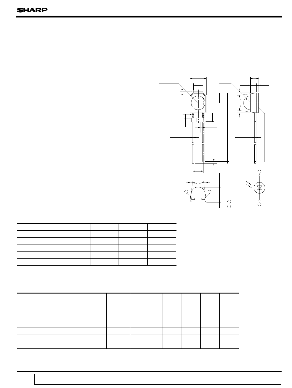
Outline Dimensions
Detector center
(blue)
2-0.45
4.0
0.4MAX.
Rest of gate
Mark
0.8
+0.2
- 0.1
(
2.54
8˚ 8˚
12
(Ta=25˚C)
˚C
˚C
2.4
±0.2
)
2.15
2-0.77
MIN.
R1.75 ±0.1
2.5
0.5
± 0.2
3.75
± 0.2
5.0
-1.0
+1.5
17.15
1 Anode
2 Cathode
8˚
8˚
2-0.4
1.5
+0.2
-0.1
2.0 ±0.2
(Unit : mm)
0.5
epoxy resin
Black visible light cut
1
2
Electro-optical Characteristics
■
Parameter Symbol
Shortcircuit current
Dark current
I
SC
I
Forward voltage V
Terminal capacitance
Peak sensitivity wavelength
Half intensity angle
Response time
*2 Ev : Illuminance by CIE standard light source A (tungsten lamp)
“ In the absence of confirmation by device specification sheets, SHARP takes no responsibility for any defects that occur in equipment using any of SHARP's devices, shown in catalogs,
data books, etc. Contact SHARP in order to obtain the latest version of the device specification sheets before using any SHARP's device.”
C
λ
∆θ - ± 45 -
, t
t
r
Conditions TYP. MAX. Unit
*2
EV= 100 lx
VR= 10V, E = 0
d
= 1mA
FIF
V
= 3V, f= 1MHz
t
R
p
f
-
RL=1kΩ, VR= 10V
MIN.
4.5 5.4 8.1
V
-10nA
-
-2035pF
-
- 200 - ns
-
-1V
960
(Ta=25 ˚C)
µ A
-nm
˚
Page 2
PD413PI
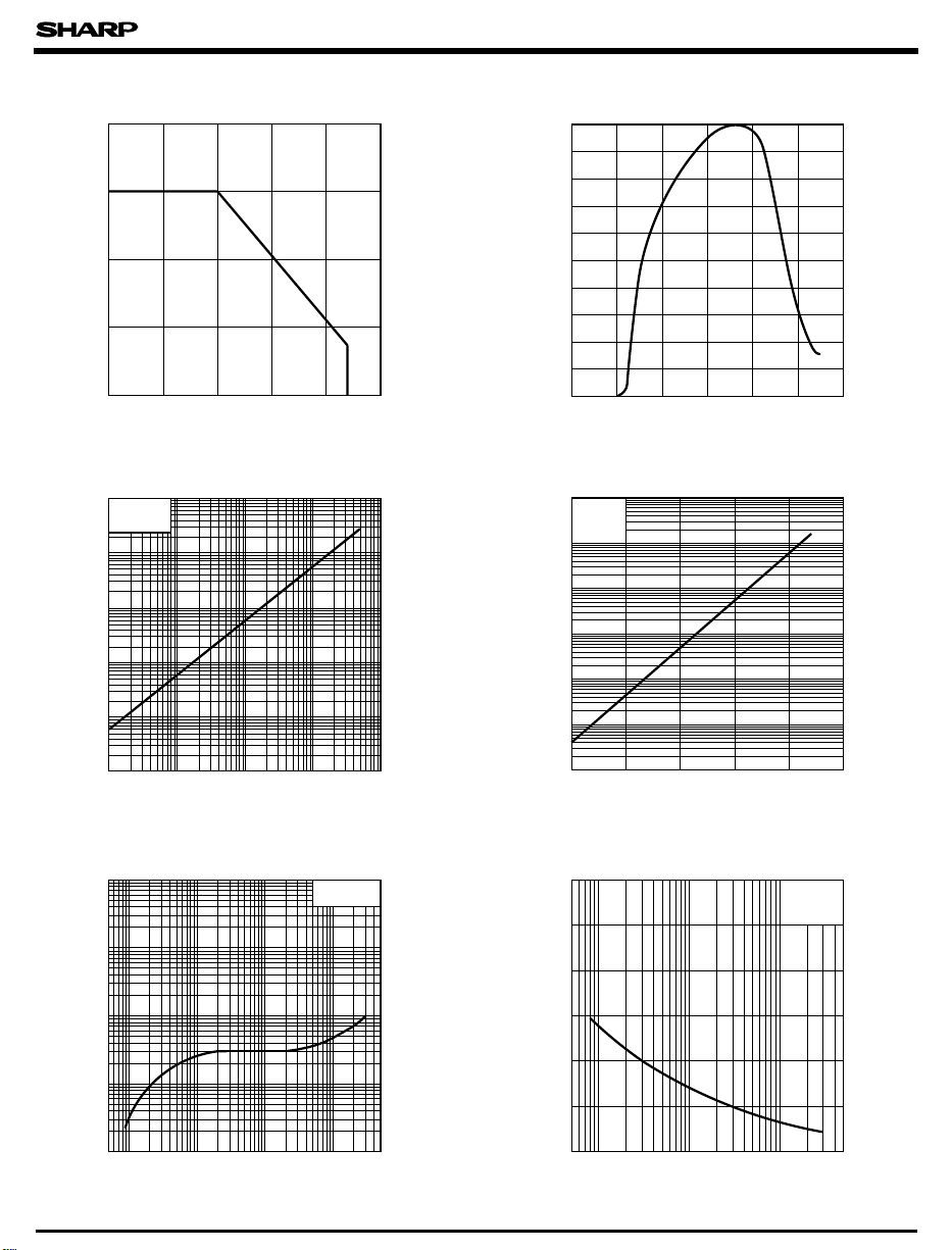
Fig. 1 Power Dissipation vs. Ambient
Temperature
200
Fig. 2 Spectral Sensitivity
100
90
150
80
70
60
100
50
40
30
50
Power dissipation P (mW)
Relative sensitivity (%)
20
10
0
-25
025
50 75 10085
Ambient temperature Ta (˚C
)
0
600 700 800 900 1 000 1 100 1 200
Wavelength λ (nm)
Fig. 3 Shortcircuit Current vs. Illuminance Fig. 4 Dark Current vs. Ambient Temperature
1 000
Ta=25˚C
100
)
µA
(
SC
10
1
0.1
Shortcircuit current I
0.01
1 10 100 1 000 10 000
Illuminance Ev (lx
)
-6
10
VR=10V
-7
10
-8
10
(A)
d
-9
10
-10
10
Dark current I
-11
10
-12
10
-25 0
25 50 75 100
Ambient temperature Ta (˚C
)
Fig. 5 Dark Current vs. Reverse Voltage Fig. 6 Terminal Capacitance vs. Reverse
-7
10
5
2
-8
10
5
(A)
d
2
-9
10
5
2
Dark current I
-10
10
5
2
-11
10
-2
525252525
10
-1
10
Reverse voltage V
0
10
(V)
R
Ta=25˚C
10
Voltage
60
50
)
pF
(
t
40
30
20
Terminal capacitance C
10
0
0.05 0.1 0.2 5 10 20 50
0.5 1 2
Reverse voltage VR(V)
f = 1MHz
Ta = 25˚C
Page 3

PD413PI
Fig. 7 Relative Output vs. Ambient Temperature
160
140
120
100
80
60
Relative output (%)
40
20
0
- 25 100
(Detector : GL537/GL538)
Test circuit
PD413PlGL537/GL538
A
Fix PD and GL at position so that distance
between them may be I =100 µ A
()
at I =20mA and Ta=25˚C
F
0 255075
Ambient temperature Ta (˚C
SC
)
Fig. 9 Relative Output vs. Distance
100
10
1
Relative output (%)
0.1
10
(Detector : GL537/GL538)
GL538
GL537
IF= 20mA
-4
-3
10
Distance between emitter and detector d (mm)
10
Ta= 25˚C
-2
-1
10
Fig. 8 Radiation Diagram
-10˚- 20˚
- 40˚
- 50˚
- 60˚
- 70˚
- 80˚
- 90˚
(
T
0
100
80
60
40
Relative sensitivity (%)
20
0
=25˚C
a
+20˚+10˚
)
+30˚- 30˚
+40˚
+50˚
+60˚
+70˚
+80˚
+90˚
Angular displacement θ
Fig. 10 Response Time vs. Load Resistance
2
10
V
= 10V
R
5
T
= 25˚C
a
2
1
10
5
(µ s)
f
,t
2
r
0
10
5
2
- 1
10
Response time t
5
2
- 2
10
10
2
25 25 25 25
10
Load resistance RL (Ω
3
10
4
10
)
5
10
Test Circuit for Response Time
I
Semiconductor laser
Pulse generator
●
Please refer to the chapter "Precautions for Use". (Page 78 to 93)
OUT
PD413PI
Output
R
L
= 0.1mA
+
10V
Input
Output
90%
10%
t
r
t
r
 Loading...