

Page 1

PD412PI
PD412PI
Compact Package Type
Photodiode with Condensing Lens
■
Features
1. High sensitivity
(TYP. 0.5A/W at λ
= 780nm)
p
2. High speed response
■
Applications
1. Optoelectronic switches
2. MD (mini disk) laser power monitors
■
Outline Dimensions
±
0.2
0.8
MAX. 0.4
Rest of gate
+0.2
- 0.1
1
4.0
2.4
2.54
❈
8˚8˚
8˚8˚
Detector center
2-0.45
±
0.1
R1.75
)
2.5
(
± 0.2
5.0
2.15
1.5-1.0
+
2-0.4
17.15
0.2
MIN. 0.5
±
3.75
*Tolerance : ± 0.15
2
* ( ) : Reference dimensions
❈ Dimension at lead root
(Unit : mm)
±
0.2
2.0
0.5
1.5
8˚
8˚
+ 0.2
- 0.1
8˚
Transparent epoxy resin
8˚
1
2
1 Anode
2 Cathode
Absolute Maximum Ratings
■
Parameter Symbol Rating Unit
Reverse voltage
Power dissipation
Operating temperature
Storage temperature
*1
Soldering temperature
*1 For MAX. 5 seconds at the position of 2.15 mm from the resin edge
“ In the absence of confirmation by device specification sheets, SHARP takes no responsibility for any defects that occur in equipment using any of SHARP's devices, shown in catalogs,
data books, etc. Contact SHARP in order to obtain the latest version of the device specification sheets before using any SHARP's device.”
V
R
P 150 mW
-25to+85
T
opr
- 40 to +100
T
stg
T
sol
(Ta=25˚C)
32 V
260 ˚C
2.15mm
˚C
˚C
Soldering area
Page 2

PD412PI
■
Electro-optical Characteristics
Parameter Symbol Conditions MIN. TYP. MAX. Unit
Shortcircuit current
Shortcircuit current temperature coefficient
Dark current
Dark current temperature coefficient
Terminal capacitance
Peak sensitivity wavelength
Peak spectral sensitivity
Response time
Rise Time
Fall Time
Half intensity angle
*2 EV : Illuminance by CIE standard light source A (tungsten lamp)
(Ta=25 ˚C)
Isc 3.5 4.7 6.3 µ A
β
I
α
C
λ
K - 0.5 - A/W
t
t
∆θ
*2
= 100 lx
E
V
*2
= 100 lx
T
d
T
t
p
E
V
VR= 10V, Ee= 0 - 0.5 10 nA
VR= 10V, Ee= 0 - 3.5 5.0
VR= 3V, f= 1MH
Z
- 0.2 - %/˚C
times/10˚C
- 100 350
- 800 - nm
l = 780nm
250
=1kΩ
r
f
R
L
VR= 10V
-
- 250 -
-
- ± 45 -
pF
ns
˚
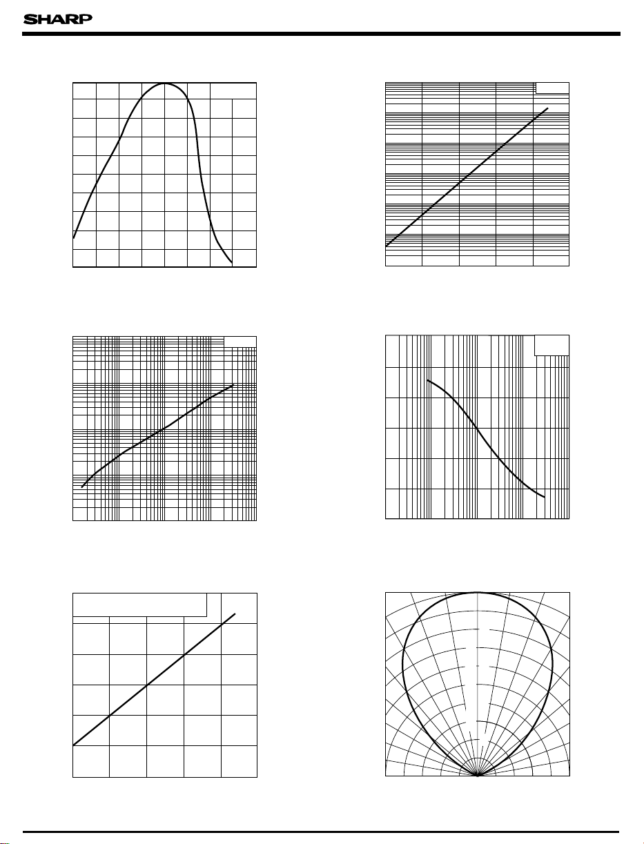
Fig. 1 Power Dissipation vs. Ambient
Temperature
200
150
100
50
Power dissipation P (mW)
0
-25
0 25 50 75 10085
Ambient temperature Ta (˚C
)
Fig. 2 Shortcircuit Current vs. Illuminance
1000
100
)
µA
(
SC
10
1
0.1
Shortcircuit current I
0.01
110
100
Illuminance EV (lx
1000
)
Ta=25˚C
10000
Page 3
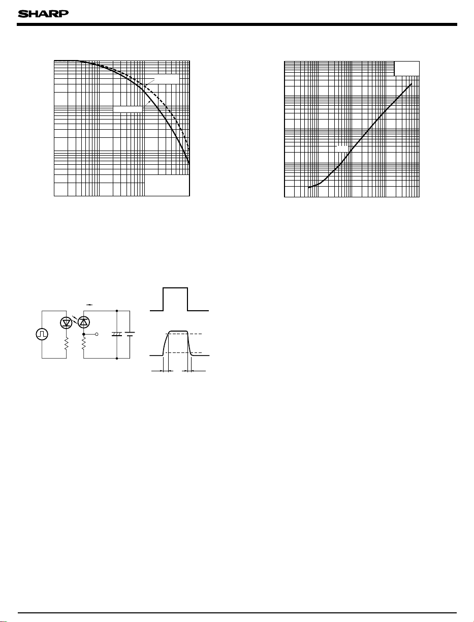
PD412PI
Fig. 3 Spectral Sensitivity Fig. 4 Dark Current vs. Ambient Temperature
-7
100
90
80
70
60
50
40
30
Relative sensitivity (%)
20
10
0
400 500
600 700 800 900 1000 1100 1200
Ta=25˚C
Wavelengthλ (nm)
Fig. 5 Dark Current vs. Reverse Voltage Fig. 6 Terminal Capacitance vs. Reverse
)
pA
(
1000
100
d
10
Ta=25˚C
10
-8
10
)
-9
A
10
(
d
-10
10
-11
10
Dark current I
-12
10
-13
10
- 25 0 25 50 75 100
Voltage
300
250
)
pF
(
t
200
150
Ambient temperature T
a
(˚C)
VR=10V
f=1MHz
Ta=25˚C
Dark current I
1
0.1
0.01 0.1 1 10 100
Reverse voltage VR(V)
Fig. 7 Relative Output vs. Ambient Temperature
115
Light source : CIE standard light
110
105
100
95
Relative output (%)
90
85
- 25 0 25 50 75 100
source A (tungsten lamp)
Ambient temperature T
a
(˚C
)
100
Terminal capacitance C
50
0
0.01 0.1 1 10 100
Reverse voltage VR(V)
Fig. 8 Radiation Diagram
0
-10˚- 20˚
100
80
-40˚
-50˚
-60˚
-70˚
-80˚
-90˚
Angular displacement θ
60
40
Relative sensitivity (%)
20
0
(
=25˚C
T
a
+10˚ +20˚
)
+ 30˚-30˚
+ 40˚
+ 50˚
+ 60˚
+ 70˚
+ 80˚
+ 90˚
Page 4
PD412PI
Fig. 9 Relative Output vs. Distance
100
10
Relative output (%)
1
0.1
10
(Detector : GL537/GL538)
GL538
GL537
= 20mA
I
F
T
-4
-3
10
Distance between emitter and detector d (m)
a
-2
10
Test Circuit for Response Time
Semiconductor laser
Pulse generator
I
OUT
PD412PI
Output
R
L
= 0.1mA
+
10V
Input
Output
t
r
= 25˚C
Fig. 10 Response Time vs. Load Resistance
100
10
)
µ s
(
f
,t
r
1
tr,t
f
0.1
Response time t
-1
10
0.01
1
10
2
10
3
10
Load resistance RL (Ω
90%
10%
t
f
VR=10V
Ta=25˚C
4
10
5
10
)
●
Please refer to the chapter "Precautions for Use". (Page 78 to 93)
 Loading...