

Page 1
®
PCM78P
16-Bit Audio
ANALOG-TO-DIGITAL CONVERTER
FEATURES
● LOW COST/HIGH PERFORMANCE 16-BIT
AUDIO A/D CONVERTER
● FAST 5
(4
µs MAX CONVERSION TIME
µs typ)
● VERY LOW THD+N ( typ –88dB at FS;
max –82dB)
±3V INPUT RANGE
●
● TWO SERIAL OUTPUT MODES PROVIDE
VERSATILE INTERFACING
● COMPLETE WITH INTERNAL REFERENCE
AND CLOCK IN 28-PIN PLASTIC DIP
±5V TO ±15V SUPPLY RANGE (600mW
●
Power Dissipation)
DESCRIPTION
The PCM78P is a low-cost 16-bit analog-to-digital
converter which is specifically designed and tested for
dynamic applications. It features very fast, low
distortion performance (4µs/–88dB THD+N typical)
and is complete with internal clock and reference
circuitry. The PCM78P is packaged in a reliable, lowcost 28-pin plastic DIP and data output is available in
user-selectable serial output formats. The PCM78P is
ideal for digital audio tape (DAT) recorders. Many
similar applications such as digital signal processing
and telecom applications are equally well served by
the PCM78P.
The PCM78P uses a SAR technique. Analog and
digital portions are efficiently partitioned into a highspeed, bipolar section and a low-power CMOS
section. The PCM78P has been optimized for excellent dynamic performance and low cost.
APPLICATIONS
● DSP DATA ACQUISITION
● TEST INSTRUMENTATION
● SAMPLING KEYBOARD SYNTHESIZERS
● DIGITAL AUDIO TAPE
● BROADCAST AUDIO PROCESSING
● TELECOMMUNICATIONS
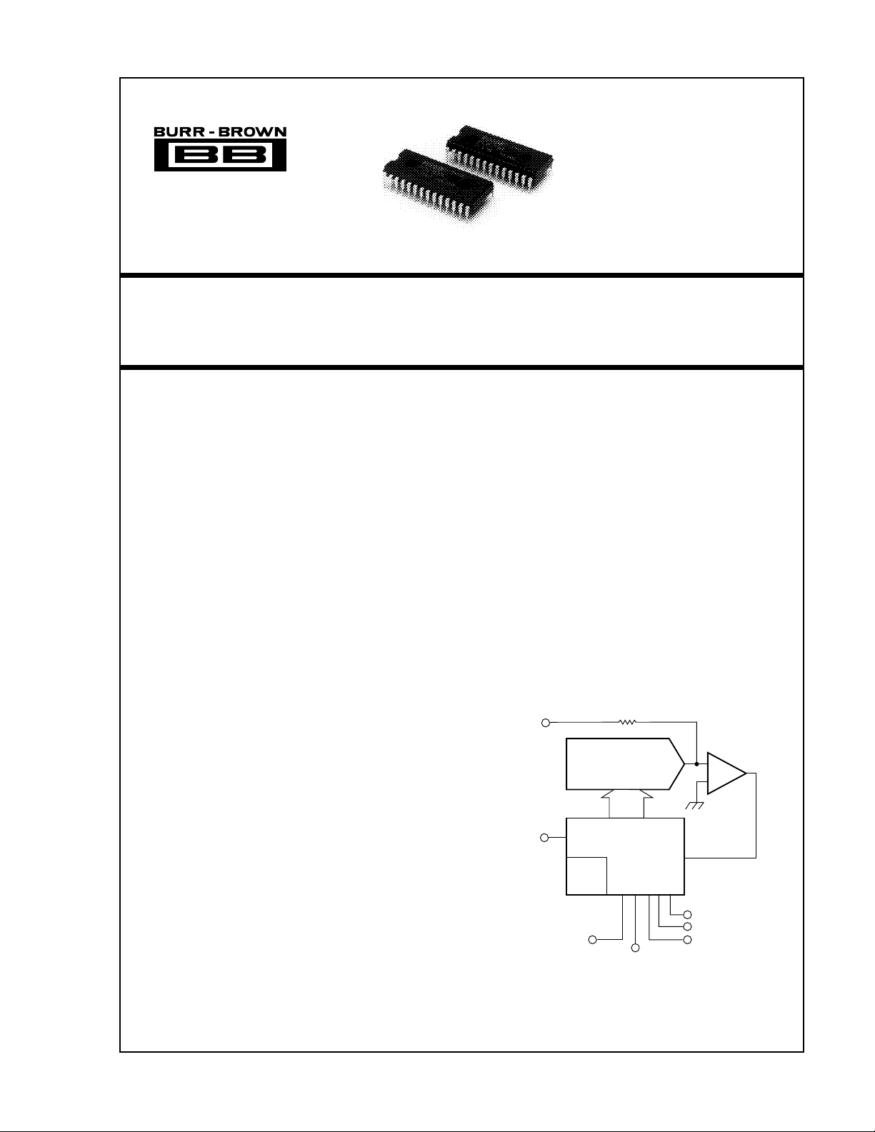
Audio Input
Convert
Command
External Clock
16-bit D/A
Converter
16-bit SAR +
Timing Control
Internal
Clock
Circuit
Status
–
Comp
+
Serial Output 1
Serial Output 2
Clock Output
International Airport Industrial Park • Mailing Address: PO Box 11400 • Tucson, AZ 85734 • Street Address: 6730 S. Tucson Blvd. • Tucson, AZ 85706
Tel: (520) 746-1111 • Twx: 910-952-1111 • Cable: BBRCORP • Telex: 066-6491 • FAX: (520) 889-1510 • Immediate Product Info: (800) 548-6132
©
1989 Burr-Brown Corporation PDS-989A Printed in U.S.A. October, 1993
Page 2
SPECIFICATIONS
ELECTRICAL
At TC = +25°C, +V
PARAMETER CONDITIONS MIN TYP MAX UNITS
RESOLUTION 16 Bits
INPUT/OUTPUT
ANALOG INPUT
Input Range –3 +3 V
Input Impedance 1.5 kΩ
DIGITAL INPUT/OUTPUT
Logic Family TTL Compatible CMOS
Logic Level: V
Data Format Serial BOB or BTC
Convert Command Negative Edge
Pulse Width 25 50 ns
CONVERSION TIME 45 µs
DYNAMIC CHARACTERISTICS
SIGNAL-TO-NOISE RATIO (SNR)
f = 1kHz (0dB) BW = 20kHz 90 dB
f = 10kHz (0dB) BW = 100kHz 80 dB
TOTAL HARMONIC DISTORTION
f = 1kHz (0dB) BW = 20kHz –91 dB
f = 19kHz (0dB) BW = 20kHz –90 dB
f = 10kHz (0dB) BW = 100kHz –90 dB
f = 90kHz (0dB) BW = 100kHz –89 dB
TOTAL HARMONIC DISTORTION + NOISE
f = 1kHz (0dB) BW = 20kHz –88 –82 dB
f = 1kHz (–20dB) BW = 20kHz –74 –68 dB
f = 1kHz (–60dB) BW = 20kHz –34 dB
f = 19kHz (0dB) BW = 20kHz –87 dB
f = 10kHz (0dB) BW = 100kHz –82 dB
f = 90kHz (0dB) BW = 100kHz –81 dB
TRANSFER CHARACTERISTICS
ACCURACY
Gain Error ±2%
Bipolar Zero Error ±20 mV
Differential Linearity Error ±0.002 % of FSR
Integral Linearity Error ±0.003 % of FSR
Missing Codes None 14 Bits
DRIFT
Gain 0°C to +70°C ±25 ppm/°C
Bipolar Zero 0°C to +70°C ±4 ppm of FSR/°C
POWER SUPPLY SENSITIVITY
+V
CC
–V
CC
+V
DD
POWER SUPPLY REQUIREMENTS
Voltage Range: +V
Current: +V
Power Dissipation ±V
TEMPERATURE RANGE
Specification 0 +70 °C
Storage –50 +100 °C
Operating –25 +85 °C
= +5V, and ±VCC = ±12V, and one minute warm-up in convection environment, unless otherwise noted.
DD
IH
V
IL
V
OH
V
OL
(2)
(5)
(6)
CC
–V
CC
+V
DD
CC
–V
CC
+V
DD
IIH = +40µA +2 +5.5 V
IIL = –100µA 0 +0.8 V
IOH = 2TTL Loads +2.4 V
IOL = 2TTL Loads +0.4 V
CONV
CONV
= 4µs
= 4µs
= 4µs
(3)
fS = 200kHz/T
fS = 200kHz/T
fS = 200kHz/T
CONV
+4.75 +15.6 V
–4.75 –15.6 V
+4.75 +5.25 V
+VCC = +12V +15 mA
–VCC = –12V –21 mA
+VDD = +5V +7 mA
= ±12V 575 mW
CC
PCM78P
(1)
±0.008 %FSR/%V
±0.003 %FSR/%V
±0.003 %FSR/%V
(4)
(7)
(8)
CC
CC
DD
NOTES: (1) When convert command is high, converter is in a halt/reset mode. Actual conversion begins on negative edge. See detailed text on timing for convert
command description when using external clock. (2) Ratio of Noise rms/Signal rms. (3) f = input frequency; f
combination); BW = bandwidth of output (based on FFT or actual analog reconstruction using a 20kHz low-pass filter). (4) Referred to input signal level. (5) Ratio
= sample frequency (PCM78P and SHC702 in
S
of Distortion rms/Signal rms. (6) Ratio of Distortion rms + Noise rms/Signal rms. (7) FSR: Full-Scale Range = 6Vp-p. (8) Typically no missing Codes at 14-bit
resolution.
®
PCM78 2
Page 3
PIN ASSIGNMENTS
PIN NAME I/O DESCRIPTION
1 Analog In I Analog Signal Input (1.5kΩ impedance).
2–V
CC
3 MSB Adjust I Internal adjustment point to allow adjustment of MSB major carry.
4+V
DD
5 No Connection — No internal connection.
6 Comparator Common I Comparator common connection. Connect to ground.
7 MSB O Parallel output of bit 1 (MSB) inverted.
8 BTC/BOB Select I Two’s complement (open) or straight binary (grounded) data output format selection.
9 Status O Output signal held high until conversion is complete.
10 Clock Out O Internal clock output generated from RC network on pins 11 and 12 (also present when external clock is used lagging
11 R
1C1
12 R
2C2
13 S
OUT2
14 +V
DD
15 S
OUT1
16 External Clock I External clock input point (internal clock must be disabled).
17 Int/Ext Clock Select I Selects either internal or external clock mode (low = internal; open = external).
18 Short Cycle I Terminates conversion at less than 16 bits (open for 16-bit mode). See text for details.
19 Convert Command I Starts conversion process (can optionally be generated internally).
20 S
21 S
22 Digital Common I Digital grounding pin.
23 +V
24 V
25 Reference Decouple I Reference decoupling point.
Latch I Latches previous conversion result for readout (must be issued with the S
OUT2
Clock I Used to read out internally latched data from previous conversion.
OUT2
CC
POT
26 Analog Common I Analog grounding pin.
27 Reference Out O 2V reference out. Should not be used except as shown in connection diagram.
28 Speed Up I Connection point for a capacitor to speed reference settling. See text for details.
NOTE: Analog and digital commons are connected internally.
I Analog power supply (–5V to –15V).
I Power connection for comparator (+5V).
external clock by ~24ns and same duty cycle).
I RC connection point used to generate internal clock. Sets clock high time. See text for details.
I RC connection point used to generate internal clock. Sets clock low time. See text for details.
O Internal shift register containing the previous conversion result. (Alternate latched data output mode).
I Power connection for +5V logic supply.
O Primary real-time data output synchronized to clock out.
clock to initiate latch and an internal convert
command).
OUT2
I Analog supply connection (+5V to +15V).
O Voltage output (~2.5V) for optional adjustment of MSB transition.
INPUT/OUTPUT RELATIONSHIPS
DIGITAL OUTPUT
ANALOG INPUT CONDITION BTC BOB
+2.999908V + Full Scale 7FFF Hex FFFF Hex
–3.000000V –Full Scale 8000 Hex 0000 Hex
0.000000V Bipolar Zero 0000 Hex 8000 Hex
–0.000092V Zero-1 LSB FFFF Hex 7FFF Hex
PACKAGE INFORMATION
MODEL PACKAGE NUMBER
PACKAGE DRAWING
PCM78P 28-Pin Plastic DIP 215
NOTE: (1) For detailed drawing and dimension table, please see end of data
sheet, or Appendix D of Burr-Brown IC Data Book.
(1)
ABSOLUTE MAXIMUM RATINGS
+V
to Analog Common .........................................................0 to +16.5V
CC
–V
to Analog Common .........................................................0 to –16.5V
CC
–V
to Analog Common ..............................................................0 to +7V
DD
Analog Common to Digital Common................................................. ±0.5V
Logic Inputs to Digital Common ................................. –0.3V to V
Analog Inputs to Analog Common .................................................. ±16.5V
Lead Temperature (soldering, 10s)................................................ +300°C
Stresses above these ratings may permanently damage the device.
DD
+ 0.5V
The information provided herein is believed to be reliable; however, BURR-BROWN assumes no responsibility for inaccuracies or omissions. BURR-BROWN assumes
no responsibility for the use of this information, and all use of such information shall be entirely at the user’s own risk. Prices and specifications are subject to change
without notice. No patent rights or licenses to any of the circuits described herein are implied or granted to any third party. BURR-BROWN does not authorize or warrant
any BURR-BROWN product for use in life support devices and/or systems.
PCM783
®
Page 4
TYPICAL PERFORMANCE CURVES
At TA = +25°C, VCC = ±15V, unless otherwise noted.
10mV
9mV
8mV
7mV
6mV
5mV
4mV
BPZ Error (mV)
3mV
2mV
1mV
0
–25 0 25 70 125
BPZ ERROR vs TEMPERATURE
Temperature (°C)
BIPOLAR GAIN ERROR as % FSR
25°C; N = 33 UNITS
18
16
14
12
10
8
6
Number of Units
4
2
0
–0.35 –0.45 –0.60
–0.40 –0.55
–0.50
% FSR
0.012
0.010
–V
CC
0.008
0.006
0.004
PSRR at +FS INPUT
0.002
% / %
–0.002
0
+V
CC
–0.004
–0.006
V
DD
–0.008
–0.010
–25 0 25 70 125
Temperature (°C)
V vs TEMP
2.002
REF
2.000
1.998
1.996
REF
1.994
V (V)
1.992
1.99
1.988
–25 0 25 70 125
Temperature (°C)
0.012
PSRR at –FS INPUT
0.01
–V
0.008
0.006
% / %
CC
+V
CC
0.004
0.002
V
DD
0
–25 0 25 70 125
Temperature (°C)
I vs SUPPLY VOLTAGE
–V
SS
CC
21
20
19
18
17
Current (mA)
16
15
+V
CC
14
41016
6 8 12 14
Supply Voltage (V)
®
PCM78 4
Page 5
DIFFERENTIAL NONLINEARITY
at 25°C
1.40
0.80
0.60
0.00
1
1.20
LSB
0.20
Major Carry Bit Number
1.00
0.40
2345678910111213141516
DIFFERENTIAL NONLINEARITY
at 0°C
1.40
0.80
0.60
0.00
1
1.20
LSB
0.20
Major Carry Bit Number
1.00
0.40
2345678910111213141516
DIFFERENTIAL NONLINEARITY
at –25°C
1.40
1.00
0.00
1
LSB
Major Carry Bit Number
1.20
0.80
2345678910111213141516
0.60
0.40
0.20
TYPICAL PERFORMANCE CURVES (CONT)
At TA = +25°C, VCC = ±15V, unless otherwise noted.
INTEGRAL NONLINEARITY
at –25°C
Major Carry Bit Number
LSB
7.00
6.00
5.00
4.00
3.00
2.00
1.00
0.00
–1.00
2345678910111213141516
1
LSB
LSB
5.00
4.00
3.00
2.00
1.00
0.00
–1.00
–2.00
5.00
4.00
3.00
2.00
1.00
INTEGRAL NONLINEARITY
2345678910111213141516
1
INTEGRAL NONLINEARITY
at 0°C
Major Carry Bit Number
at 25°C
0.00
–1.00
–2.00
2345678910111213141516
1
Major Carry Bit Number
®
PCM785
Page 6

TYPICAL PERFORMANCE CURVES (CONT)
At TA = +25°C, VCC = ±15V, unless otherwise noted. Histograms done with conversion time = 8µs.
LSB
LSB
7.00
6.00
5.00
4.00
3.00
2.00
1.00
0.00
3.00
2.00
1.00
0.00
–1.00
–2.00
–3.00
–4.00
–5.00
–6.00
–7.00
INTEGRAL NONLINEARITY
2345678910111213141516
1
INTEGRAL NONLINEARITY
2345678910111213141516
1
at 70°C
Major Carry Bit Number
at 125°C
Major Carry Bit Number
LSB
LSB
DIFFERENTIAL NONLINEARITY
1.80
1.60
1.40
1.20
1.00
0.80
0.60
0.40
0.20
0.00
2345678910111213141516
1
DIFFERENTIAL NONLINEARITY
2.50
2.00
1.50
1.00
0.50
0.00
1
2345678910111213141516
at 70°C
Major Carry Bit Number
at 125°C
Major Carry Bit Number
INTEGRAL NONLINEARITY ERROR
1.50
1.00
0.50
0.00
–0.50
Differential
–1.00
–1.50
–2.00
–8192 0.000 8192
–4096 4096
®
(to 14-Bit LSB)
BIN
PCM78 6
DIFFERENTIAL NONLINEARITY ERROR
2.00
1.50
1.00
0.50
LSB
0.00
–0.50
–1.00
–8192 0.000 8192
–4096 4096
(to 14-Bit LSB)
BIN
Page 7

TYPICAL PERFORMANCE CURVES (CONT)
0
–20
–40
–60
–80
–100
–120
–140
0 50 100
Frequency (kHz)
Magnitude (dB)
25 75
At TA = +25°C, VCC = ±15V, unless otherwise noted. Histograms done with Conversion Time = 8µs.
0
SPECTRAL RESPONSE, f
–20
–40
–60
Input Frequency 976.6Hz
Fund: –0.07dB 6th: –135.02dB
2nd: –87.80dB THD: –87.10dB
3rd: –97.43dB SNR: 81.05dB
4th: –102.35dB SINAD: 80.09dB
5th: –107.86dB
–80
Magnitude (dB)
–100
–120
–140
0 50 100
25 75
Frequency (kHz)
SPECTRAL RESPONSE, f
0
–20
–40
–60
Input Frequency 976.6Hz
Fund: –20.07dB 6th: –110.06dB
2nd: –108.36dB THD: –76.75dB
3rd: –100.44dB SNR: 61.79dB
4th: –111.52dB SINAD: 61.65dB
5th: –102.06dB
–80
Magnitude (dB)
–100
–120
–140
0 50 100
25 75
Frequency (kHz)
≈ 1kHz
IN
≈ 1kHz
IN
SPECTRAL RESPONSE, f
IN
Input Frequency 19970.7Hz
Fund: –0.08dB 6th: –101.44dB
2nd: –92.21dB THD: –88.12dB
3rd: –91.59dB SNR: 79.25dB
4th: –101.23dB SINAD: 78.72dB
5th: –109.32dB
–20
–40
–60
0
SPECTRAL RESPONSE, f
Input Frequency 19970.7Hz
Fund: –19.94dB 6th: –107.32dB
2nd: –105.69dB THD: –72.81dB
3rd: –95.90dB SNR: 61.60dB
4th: –106.71dB SINAD: 61.28dB
5th: –97.57dB
IN
–80
Magnitude (dB)
–100
–120
–140
0 50 100
25 75
Frequency (kHz)
≈ 20kHz
≈ 20kHz
0
–20
–40
–60
–80
Magnitude (dB)
–100
–120
–140
0 50 100
SPECTRAL RESPONSE, f
≈ 1kHz
IN
Input Frequency 976.6Hz
Fund: –60.06dB 6th: –106.00dB
2nd: –109.18dB THD: –42.15dB
3rd: –108.31dB SNR: 21.73dB
4th: –134.66dB SINAD: 21.69dB
5th: –114.73dB
25 75
Frequency (kHz)
0
SPECTRAL RESPONSE, f
IN
Input Frequency 19970.7Hz
–20
–40
–60
–80
Magnitude (dB)
–100
–120
–140
0 50 100
Fund: –59.96dB 6th: –110.11dB
2nd: –109.09dB THD: –41.60dB
3rd: –124.49dB SNR: 21.93dB
4th: –116.40dB SINAD: 21.88dB
5th: –112.18dB
25 75
Frequency (kHz)
PCM787
≈ 20kHz
®
Page 8

TYPICAL
THEORY OF OPERATION
PERFORMANCE CURVES
At TA = +25°C, VCC = ±15V, unless otherwise noted.
0.008
0.007
THD+N (%)
0.006
0.005
2610
0.051
0.050
0.049
0.048
THD+N (%)
0.047
0.046
0.045
2610
5.2
5.0
4.8
THD+N (%)
4.6
4.4
2610
THD+N vs CONVERSION TIME (0dB)
48
Convert Time (µs)
THD+N vs CONVERSION TIME (–20dB)
48
Convert Time (µs)
THD+N vs CONVERSION TIME (–60dB)
48
Convert Time (µs)
(CONT)
The PCM78P is a successive approximation A/D converter;
this type of converter is well suited to high speed and
resolution. The accuracy of a successive approximation
converter is described by the transfer function shown in
Figure 1. All successive-approximation A/D converters
have an inherent quantization error of ±1/2LSB. The
remaining errors in the A/ D converter are combinations of
analog errors due to the linear circuitry, matching and
tracking properties of the ladder and scaling networks,
power supply rejection, and reference errors. In summary,
these errors consist of initial errors including Gain, Offset,
Linearity, Differential Linearity, and Power Supply Sensitivity. Gain drift over temperature rotates the line (Figure 1)
about zero, and Offset drift shifts the line left or right over
the operating temperature range. Total Harmonic Distortion
+ Noise (THD+N) is a measure of the magnitude and
distribution of the Linearity Error, Differential Linearity
Error, and Noise, as well as quantization errors. The
THD+N specification is most useful in audio or dynamic
signal processing applications. To be useful, THD+N
should be specified for both high level and low level input
signals. This error is unadjustable and is the most meaningful indicator of A/D converter accuracy for dynamic
applications.
DYNAMIC RANGE
Dynamic range is a measure of the ratio of the smallest
signals the converter can resolve to the full scale range and
is usually expressed in decibels. The theoretical dynamic
range of a converter is approximately 6 x n, where n is the
number of bits of resolution. A 16-bit converter would thus
have a theoretical dynamic range of 96dB. The actual useful
dynamic range is limited by noise and linearity errors and
is therefore somewhat less than the theoretical limit.
0111…1111
0111…1110
0000…0010
0000…0001
0000…0000
1111…1111
1111…1110
Digital Output (BTC Code)*
1000…0001
1000…0000
–FSR
(
2
*See Input/Output Relationship Table for code definitions.
–1/2LSB
Offset
Error
All Bits Off
Analog Input
OffINE
)
All Bits On
Gain
Error
+1/2LSB
OnINE
+FSR
–1LSB
()
2
FIGURE 1. Input vs Output for Ideal Bipolar A/D Converter.
®
PCM78 8
Page 9

B&K
Digital
Oscillator
SHC702
PCM78
Serial-To-Parallel
0
–20
–40
–60
–80
Signal Level (dB)
–100
–120
25
Frequency (kHz)
Sync
50 750.0 100
Convert Command
Analyzer Software
DataPhysics Corp
FIGURE 2. Block Diagram of Distortion Test Circuit.
DISCUSSION OF
SPECIFICATIONS
TOTAL HARMONIC DISTORTION
Evaluating distortion specifications can be a difficult task,
as distortion is often specified in different ways. Total
Harmonic Distortion (THD) is defined as the ratio of the
square root sum of the squares of the value of rms harmonics
to the value of the rms fundamental and is expressed in
percent or dB. Note that this measurement only includes
energy present in those frequencies which would contain
harmonics, and therefore is less than Total Harmonic
Distortion plus Noise.
The Total Harmonic Distortion plus Noise (THD+N) is
defined as the ratio of the square root of the sum of the
squares of the value of the rms harmonics and rms noise to
the value of the rms fundamental and is expressed in percent
or dB. This is the most meaningful measurement of a
dynamic converter’s performance because it includes all
energy present in the signal that is not fundamental. A block
diagram of the test circuit used to measure the THD and
Timing
Digital Distortion
THD+N of the PCM78 is shown in Figure 2. This digital
system is capable of differentiating harmonic energy and
noise; conventional distortion analyzers which operate on a
tracking notch filter principle cannot distinguish this energy,
and therefore only measure THD+N. Unfortunately, in the
past, these systems were used for measuring distortion
performance of converters, and the distortion was often
simply specified as “THD”, when in fact it was really
THD+N. For this reason, it is often confusing to compare
specifications of converters unless one knows exactly what
was being measured.
If we assume that the error due to the test circuit of Figure
2 is negligible, then the rms value of the PCM78 error
referred to the input can be shown to be
where N is the number of samples, E
error at each sample, E
THD+N =
IEEE-488
Communication
HP-330
Scientific
Computer
N
1
EL(i)+EQ(i)+EN(i)
∑
[]
N
i=1
E
rms
(i) is the quantization error at each
Q
2
X 100%
(i) is the linearity
L
B&K
Digital
Oscillator
Sync
2
1
0
Error (LSB)
–1
–2
0
2048
1024
Codes
4095
3072
FIGURE 3. Block Diagram of Histogram Test.
SHC702
Convert Command
Timing
HP-330
Scientific
Computer
PCM78
Serial-To-Parallel
64k
Memory
IEEE-488
®
PCM789
Page 10

MSB Adjust
Status
BSC
Timing
Control
Logic
Latch
74LS164
74LS273
Latch Enable
D
16-Bit
DAC
Deglitcher Control
Deglitcher
Shibasoku
AG16A
or
Equivalent
Low-Pass
Filter
Program-
mable
Gain Amp
Distortion
Tester
S/H
Amplifier
S/H Control
Audio
Oscillator
Shibasoku
AG16A
or
Equivalent
DUT
PCM78P
Convert
Command
A
FIGURE 4. Production Distortion + Noise Test System Block Diagram.
For the PCM78 the test sampling frequency was chosen to
Reference
Clock
be 200kHz, near the PCM78’s fastest rate of conversion.
The test frequencies used vary within the audio range, and
are stepped in amplitude from 0dB, to –20dB, to –60dB.
A(S/H)
B
(CC)
S
(Status)
(Clock)
C
(Data Latch)
D
(Deglitcher
Control)
50ns
<8µs
1 2 3 4 151617
500ns
8.5µs
In manufacturing the PCM78, the test system shown in
Figure 4 is used to test for guaranteed THD+N.
ACCURACY VS CONVERSION
TIME AND INPUT SIGNAL LEVEL
The relationship of THD vs input signal level and THD vs
conversion time is shown is the typical curves. Slowing the
conversion time to more than 8µs results in little added
benefit in terms of THD+N.
For applications which are not as concerned with dynamic
performance but require DC accuracy and linearity, it is
best to use the PCM78 at the longest conversion time
possible for the system requirements. Slowing the PCM78
FIGURE 5. Timing Diagram for Figure 4.
sample, and EN(i) is the residual noise energy present at
each sample. Similarly, THD alone can be expressed as
THD =
N
1
∑
N
i=1
E
()
ELi
rms
2
X 100 %
to 8µs-10µs conversion time results in a substantial improvement in linearity. The typical curves show DNL and
INL plots for a typical device, at an 8µs conversion time.
Due to the segmented architecture of the internal DAC used
in the successive approximation conversion technique, significant differential linearity errors occur near bits 3 and 4.
Allowing more settling time for the DAC (by slowing the
conversion speed) will improve this differential linearity
error and give equivalent performance to more costly DCspecified 12-bit to 14-bit A/D converters.
These expressions indicate that there is a correlation between THD+N and the square root of the sum of the squares
of the linearity errors at each digital word of interest. In
order to find this error at each code, a histogram test must
be performed on the PCM78, as illustrated in Figure 3. The
histogram for every converter is unique, as the linearity
errors from converter to converter will vary in their placement along the transfer function. Typical histogram data is
shown in the Typical Curves.
However, this expression for THD+N does not mean that
the worst case linearity error of the A/ D is directly correlated to the THD+N because the digital output words from
theA/ D vary according to the amplitude and frequency of
the sine wave input as well as the sampling frequency.
®
SYSTEM DESIGN
CONSIDERATIONS
DIGITAL CIRCUIT CONNECTIONS
The PCM78 comes complete with an internal clock circuit,
or it may be clocked by an external clock. Choosing which
mode to operate with depends upon the application for
which the PCM78 will be used. In an application where the
sample rate may not be fixed (transient recording, etc.),
using the internal clock set to give a very fast conversion
may be the best solution. In systems where the sample rate
is fixed, an external clock is probably the better choice since
it will allow the digital system design to be synchronous.
PCM78 10
Toko Model
298BLR-002N
or PCM11 or
Equivalent
LOW-PASS FILTER
0
20
40
60
80
Attenuation (dB)
100
120
1 100
CHARACTERISTICS
10
Frequency (MHz)
Page 11

In either case, the PCM78 requires 17 clock cycles to
complete a conversion. To calculate the clock frequency
necessary for a given conversion time, the following equation may be used:
f
CLOCK
=
17
Conversion Time
The internal clock operates only during a conversion, and is
gated on by the falling edge of the convert command. See
Figure 6. The internal clock is available on pin 10, Clock
Out. The high and low time of this clock is set by R
R
respectively. The duty cycle of the clock should be
2C2
1C1
and
between 20% to 80%, and may be set to 50% for simplicity.
Clock High Time (in ns) = 1.32R
Clock Low Time (in ns) = 1.32R2C
1C1
2
R in kΩ; C in pF.
These equations are approximate (±5%); they should be
used for determining an initial part value which will then
need to be “tweaked” for accurate timing. If highly accurate
time bases are required, use of an external clock is recommended.
The external clock is applied at pin 16, and the Int/Ext
Clock select (pin 17) should be left open (an internal pullup resistor assures that the logical state of an open pin is
“1”). Using the external clock requires careful placement in
time of the convert command. Figure 7 diagrams the recommended timing with an external clock. A simple circuit
which assures the proper timing of the convert command is
shown in Figure 8.
Due to the design of the Clock/Logic chip in the PCM78, a
conversion is begun inside the PCM78 by an asynchronous
state machine. This places stringent requirements on the
timing of the convert command, as improper timing can
cause metastable states within this state machine. Using the
circuitry shown in Figure 8, the user is assured of consistent
operation, and these invalid states within the state machine
are entirely avoided. (Note that this is not a consideration
when using an internal clock, as nothing is being clocked
when a convert command is presented to the PCM78).
The Clock Out function is a gated form of the external
clock, i.e. the 17 clock cycles used in the conversion are
present on this pin during conversion. This allows use of a
continuous external clock, with Clock Out being the clock
that the converter is actually using for conversion. Note that
this is simply a delayed (~24ns) version of the external
clock, and will have the same frequency and duty cycle.
The S
Latch enables the user to latch data from the
OUT2
previous conversion and read it out at a higher speed than
the convert clock. This feature allows the converter to
easily interface to digital filtering necessary for
oversampling. See Figure 9 for timing information in this
mode.
In this mode, the PCM78 generates its own internal convert
command when the S
Latch going low; the external convert command may
S
OUT2
Clock goes high within ±50ns of
OUT2
not be used, and pin 19 must be grounded. The timing
diagram shows the recommended timing for using this
mode. After the S
from the SAR is loaded into the S
rising edge of the S
Latch control signal goes low, data
OUT2
Clock. This clock edge should
OUT2
latch on the next
OUT2
occur prior to the next rising edge of the conversion clock
(internal or external), since the SAR will reset itself prior to
the latching
Convert
Command
Clock Out
Status
S
OUT 1
Data
T
1
T
3
T
T
4
2
T
5
T
6
PCM78 TIMING SPECIFICATIONS
TA = +25°C, VDD = +5V, guaranteed by sample testing; these parameters are not 100% tested in production.
TIME (ns)
TIME DESCRIPTION MIN TYP MAX
CONVERT COMMAND pulse width 25 50
T
1
T
Delay from falling edge of CONVERT COMMAND to rising edge of CLOCK OUT 60 70 85
2
Delay from rising edge of CLOCK OUT to rising edge of STATUS 8 10 30
T
3
INTERNAL CLOCK pulse width 50 125 450
T
4
INTERNAL CLOCK period 140 290 500
T
5
Delay from rising edge of CLOCK OUT to bit data valid 17 20 50
T
6
Delay from rising edge of 17th clock pulse to falling edge of STATUS 10 15 30
T
7
NOTE: (1) When using the internal clock, the clock does not operate until the Convert Command is low. It is therefore possible to keep the convert command
high indefinitely, thereby keeping the PCM78 in a halt mode. The conversion cycle begins on the falling edge of convert command, and convert command must
remain low during the entire conversion cycle in order to make the PCM78 operate properly.
FIGURE 6. Conversion Timing when using Internal Clock.
PCM7811
T
7
(1)
®
Page 12

T
Clock
PCM78
Clock (Ext)
Sample
(Convert)
Q
1
Q
2
Q
3
Convert
Command
Ext
Clock
Convert
Command
Clock Out
Status
S
OUT 1
Data
1
T
2
T
5
T
3
T
4
T
6
T
7
T
8
T
9
PCM78 TIMING SPECIFICATIONS
TA = +25°C, VDD = +5V, guaranteed by sample testing; these parameters are not 100% tested in production.
TIME (ns)
TIME DESCRIPTION MIN TYP MAX
EXTERNAL CLOCK pulse width 50 125
T
1
T
EXTERNAL CLOCK period 140 290
2
T
Delay from falling edge of EXTERNAL CLOCK to rising edge of CONVERT COMMAND –30 0 420
3
CONVERT COMMAND pulse width 10 50 200
T
4
Delay from falling edge of CONVERT COMMAND to rising edge of EXTERNAL CLOCK 20 50 430
T
5
Delay from falling edge of CONVERT COMMAND to rising edge of CLOCK OUT 40 75 460
T
6
Delay from rising edge of CLOCK OUT to rising edge of STATUS 6 10 30
T
7
Delay from rising edge of CLOCK OUT to bit data valid 15 17 20
T
8
Delay from rising edge of 17th clock pulse to falling edge of STATUS 8 10 30
T
9
NOTE: (1) The PCM78 does not contain dynamic digital circuitry, and can be clocked as slowly as the user wishes. In typical applications, the longest clock
period may be as long as 1µs.
(1)
(1)
FIGURE 7. Conversion Timing when using External Clock.
if the convert clock rises before the S
condition is avoided as long as the frequency of S
Clock. This
OUT2
OUT2
is at least 1.5 times that of the conversion clock.
The internal convert command is generated upon S
Clock
OUT2
The data read out on S
previously performed, while the data that is present on
S
is the real time readout of the successive approxima-
OUT1
tion as it occurs.
Latch going low, and its falling edge occurs upon the first
falling edge of S
Latch should remain low for at least 2 cycles of S
S
OUT2
Clock after S
OUT2
Latch goes low.
OUT2
OUT2
Clock to insure proper latching. In many applications, the
Latch can be the 2fS signal present in many digital
S
OUT2
audio systems, typically known as WDCK. Figure 10
includes an example of this application.
SHORT CYCLE
The PCM78 has the ability to be short cycled to a resolution
less than 16 bits. This is accomplished by driving the Short
Cycle pin (pin 18) low when the conversion is to be
terminated, and holding it low until the next convert
command is given. The circuit in Figure 11 will accomplish
this function.
Convert
Q
2
Command
Q3
Q
+5V
Sample
(Convert)
DQCDQCD
PCM78
Clock
(Ext)
Q
1
Clock
FIGURE 8. Convert Command Timing Circuit for Use with External Clock.
®
PCM78 12
is from the conversion
OUT2
Page 13

S
OUT 2
Clock
Ext
T
2
T
T
4
3
Clock
Status
T
S
OUT 2
Latch
S
OUT 2
Data
S
OUT 1
Data
1
Data (n – 1)
MSB
LSB
Data Sample n
MSB MSBLSB
Data n
MSB
Data (n + 1)
TA = +25°C, VCC = +5V, guaranteed by sample testing; these parameters are not 100% tested in production.
TIME (ns)
TIME DESCRIPTION MIN TYP MAX
S
T
1
T
2
T
3
T
4
Latch pulse width 50 100
OUT2
S
Clock Cycle 24
OUT2
Delay from rising edge of CLOCK OUT to bit data valid 10 30
Delay from rising edge of S
Clock to rising edge of Ext Clock 50 125
OUT2
FIGURE 9. Timing when using S
OUT2
Latch.
WDCK
(S Latch)
OUT 2
(2f )
S
Ext Clock
128
f
S
)(
3
Word A’s Serial Data
Serial Out 1 MSB LSBMSB LSB
S Clock
OUT 2
128
f
S
)(
2
Serial Out 2
FIGURE 10. Application Example of S
OUT 2
+5V
1
A
2
CL
13
A
12
CL
PCM78P
10
Clock Out
Convert Command
19
LS20
LS393
Operation.
Jumper
3
Q
A
4
Q
B
5
Q
C
6
Q
D
11
Q
E
+5V
B1 Word
Word A’s Serial Data
Word A's Serial Data
MSB LSB MSB LSB
10kΩ x 4
NO OF BITS
JUMPER
12345
1
LS20
(PCM78)
18
Short
Cycle
2
3
4
5
15 X X X X 0
14 0000X
13 X000X
12 0 X 0 0 X
11 X X 0 0 X
10 0 0 X 0 X
9X0X0X
80XX0X
X: Off 0: On
FIGURE 11 . Short Cycle Circuit.
CC
1234111213 111213123
Clock
Short
Cycle
Status
Conversion
Time
FIGURE 12. Short Cycle Operation Timing.
®
PCM7813
Page 14

If Short Cycle is not held low until the next convert
command is issued, the Status line will go high in
synchronization with Short Cycle. This is because the
operation of the Status line becomes invalid after Short
Cycle is asserted. An example of the Short Cycle operation
is shown in Figure 12.
In those systems where a user may not be using a continuous
external clock, it is necessary to assure that a falling edge
of external clock occurs after short cycle goes low. This is
because conversion actually stops on the first falling edge
of external clock after Short Cycle goes low.
ANALOG CIRCUIT CONSIDERATIONS
Layout Precautions
Analog and Digital Common are connected internally in the
PCM78, and should be connected together as close to the
unit as possible, preferably to a large ground plane under the
ADC. Low impedance analog and digital common returns
are essential for low noise performance. Coupling between
analog inputs and digital lines should be minimized by
careful layout. The input pin (pin 1) and the MSB adjust pin
(pin 3) are both extremely sensitive to noise; digital lines
should be kept away from these pins to avoid coupling
digital noise into the sensitive analog circuitry.
Contact factory for a recommended PCB layout for the
PCM78.
Power Supply Decoupling
The power supplies should be bypassed with tantalum or
electrolytic capacitors as shown in Figure 13 to obtain noise
free operation. These capacitors should be located as close
to the ADC as possible. Bypass the 1µF electrolytic
capacitors with 0.01µF ceramic or polystyrene capacitors
for improved high frequency performance.
+V
CC
+
+
decoupling capacitor should range from 0.1µF to 4.7µF;
larger values can cause reference settling problems which
may manifest themselves as missing codes. This capacitor
should be as close to the PCM78 as possible, to minimize
the potential for coupling noise into the device; with a good
board layout it may be best to leave this capacitor out of the
circuit altogether, as the extra lead length may only cause
more noise in the reference.
Pin 27 is a decoupling point to ground, as well as the output
of the 2V reference. This point should not be used to supply
reference voltage to external circuitry unless it is buffered.
A 2.2µF capacitor is recommended, and the capacitor used
here should not exceed 4.7µF.
Pin 28, the Speed Up pin, allows a capacitor to be connected
to ground to facilitate reference settling. This does not speed
up the conversion time, but it does reduce odd order
harmonic distortion. As with the decoupling capacitor on
pin 25, this may also contribute to noise; if harmonic content
is most important in an application, this capacitor (0.1µF 10µF) should be connected. In all other cases, it is best to
leave the capacitor out of the circuit.
Input Scaling
The analog input should be scaled as close to the maximum
input signal range as possible in order to utilize the
maximum signal resolution of the A/D converter. The DAC
inside the PCM78 has a ±2mA range, and the nominal ±3V
input is scaled by a 1.5kΩ resistor. In order to scale to other
ranges, see Table I for recommended scaling resistor values,
connected as shown in Figure 14.
INPUT RANGE R
±10V 8.2kΩ
±5V 3.3kΩ
NOTE: R values shown assume use of 1k trim pot to adjust for scale
accuracy.
TABLE I. PCM78 Input Scaling Resistor Values.
.01µF
1µF
23
PCM78
+
1µF
2
–V
4
.01µF
CC
+V
DD
+
.01µF
1µF
+
FIGURE 13. Recommended Power Supply Decoupling.
Reference Decoupling and Speed Up
In order to assure the lowest noise operation of the PCM78,
the reference may be bypassed by three different capacitors.
Pin 25 is a decoupling point for the reference to –V
®
CC
. The
PCM78 14
*1kΩ
*Use to trim for exact scaling. Use
trim pot with temperature coefficient
of 100ppm/°C or better.
R
1
PCM78
FIGURE 14. PCM78 Input Scaling Circuit.
INPUT IMPEDANCE
The input signal to the PCM78 should come from a low
impedance source, such as the output of an op amp, to avoid
any errors due to the dynamic input impedance that a
successive-approximation converter presents to the outside
world because of the changing currents in this circuit during
conversion as the converter steps through its approximations.
If the driving circuit output impedance is not low, a buffer
amplifier should be added between the input signal and the
direct input to the PCM78 as shown in Figure 15.
Page 15

S
D
Q
Q
Clk
R
S
D
Q
Q
Clk
R
+5V
+5V
Status
Clk Out
OUT1
S
Data In
ICK
ILD
NOTE: Set for
16-Bit external
ILD, ICK MSB
bit first
PCM78P DSP32C
–
S
D
Q
Q
Clk
R
S
D
Q
Q
Clk
R
+5V
+5V
+5V
+5V
Status
Clk Out
OUT1
S
DR
Clk R
FSR
NOTE: FSM = 1
PCM78P
TMS320C25/C30
V
IN
+
OPA627
1
PCM78
FIGURE 15. Buffer Amplifier for PCM78 Input.
MSB Adjustment
Differential Linearity errors at bipolar zero and THD are
guaranteed to meet data sheet specifications without any
external adjustment. However, a provision has been made
for an optional adjustment of the MSB linearity point which
makes it possible to eliminate DLE error at BPZ. This is
important when the signal level is very low, because zero
crossing noise (DLE at BPZ) becomes very significant when
compared to the small codes changes occurring in the LSB
portion of the converter.
The PCM78 is laser trimmed for best performance at the
factory without the MSB adjust circuitry installed; if better
performance can be obtained it would be by the addition of
the MSB adjust circuitry shown in Figure 16.
The best method of adjusting the MSB is by using a real time
FFT routine to monitor the levels of odd order harmonics
when a sine-wave is being digitized by the PCM78.
Adjusting the potentiometer in Figure 16 will allow the user
to reduce the magnitude of odd-order harmonics.
An alternate method is to reconstruct the data out of the
PCM78 through a DAC, and measure THD+N on a
conventional distortion analyzer. Adjust the potentiometer
for minimum THD+N.
FIGURE 17. PCM78 Interface to TMS320C25/C30 DSP
Processors.
Q
Q
RXD
RXC
DSP56001
FSR
NOTE: FSM =
Bit Mode
S
Clk Out
PCM78P
Status
OUT1
+5V
D
Clk
+5V
+5V
S
Q
Q
R
+5V
D
Clk
S
R
FIGURE 18. PCM78 Interface to Motorola DSP56001 DSP
Processor.
–V
CC
2
MSB ADJ
3
200kΩ
1MΩ
FIGURE 16. MSB Adjust Circuit.
APPLICATIONS INFORMATION
A typical digitization circuit, used on the demonstration
board available for the PCM78, is shown in Figure 20. The
connections and part values shown in this circuit have been
optimized for the best THD+N performance at a 200kHz
sample rate.
The PCM78 may be interfaced to many popular digital
signal processors, such as the TMS320, DSP56001, and the
DSP32. Suggested interface circuits for these processors are
shown in Figures 17-19.
220kΩ
V
POT
24
FIGURE 19. PCM78 Interface to AT&T DSP16 & DSP32C
Processors.
®
PCM7815
Page 16

C20C
+5
+5
GND
1
–5+5+15
–15
6543
87
9
10
18 17 16 15 14 13 12 11
2
5 6
4
1 2 3
B1
B2
B3
B4
B5
B6
B7
B8
P2
B9
B10
B11
B12
B13
B14
B15
B16
DV
P1
–5
GND
+5
+15
GND
–15
Reconstructed
Output
3
J
17
910111315
+
+
2.2µF
2.2µF
2.2µF
+
19
18
C
C
RF
OUT
V
8316
CLK
1
5
2.2µF
+
SJ
PCM56
7
I
DATA
14
OUT
122
ADJ
Trim
MSB
U5
LE
6
8
U4
9
+5
1
OUT
S
+5
10
U4
CLK
5
6
Q
Q
111412
7
U3
+5
2
74HCT74
3
+5
16
C
+
2.2µF
U4
14
1
2
7
HCT14
11
U4
HCT14 HCT14 HCT14
13
6
U4
512
4
U4
HCT14 HCT14
3
101316
GH
+
2.2µF
21
C
+
2.2µF
22
C
F
E
U7
D
74HC594
BC
RCK
8
A
SER
SRCK
151234567
12
14
11
9
101316
QH
GH
F
E
4567
U6
D
74HC594
BC
RCK
8
A
SER
SRCK
15123
12
14
11
+15
–15
15
C
11
C
+
2.2µF
+5
3
C
+
2.2µF2.2µF
+
2
2.2µF
C
1
R 20kΩ
1
+
C
+5
–5
9
11
43
+
+
8
C
7
+
C
U1
SHC5320
2.2µF
2.2µF
2.2µF
100pF
+
2
2
R
10
15
9
23
Out
Out 1
Serial
14
4
ANALOG In Clock
2
1
Status
POT
MSB Adj
V
3
24
JP7
JP8
10
R
11
R
200kΩ
3.3kΩ
100kΩ
4
R
7
68
–
1
14
1.5kΩ
6
R
3kΩ
1
R
J1
9
R
TP1
7
27
+
13
C
3.3kΩ
R
3
MSB
REF Out
Ω
3k
Speed Up
28
2.2µF
TP2
16
EXT CLK
CR
CR
25
1
2
TP6
20
2
OUT
S
REF
Latch
DCPL
21
2
OUT
S
+5
+5
+5
IN4148IN4148
TP4
18
Clock
Short Cycle
Comparator
Common8BOB/BTC SEL
6
5
+5
JP
4
2.2µF
+
14
U8
3
Ω
3.3k
5
R
12
U8
Ω
3.3k
13
6
R
2
U8
1
13
2
OUT
S
7
HCT05HCT05HCT05
4
C
7
100pF
2622
19
INT External Clock
13
17
RC1
RC2
11
12
3.3kΩ
11
12
R
JP
JP
Ω
2
RV 1k
3
RV 1kΩ
JP
Ω
7
R
C
910
C
3.3k
100pF
100pF
+5
2
J
Convert
Command
+5
Status
Input
Analog
®
PCM78 16
FIGURE 20.Schematic for Demonstration Board (DEM1122).
 Loading...