

Page 1
®
PCM61P
1
©
1989 Burr-Brown Corporation PDS-972E Printed in U.S.A. October, 1993
PCM61P
Serial Input 18-Bit Monolithic Audio
DIGITAL-TO-ANALOG CONVERTER
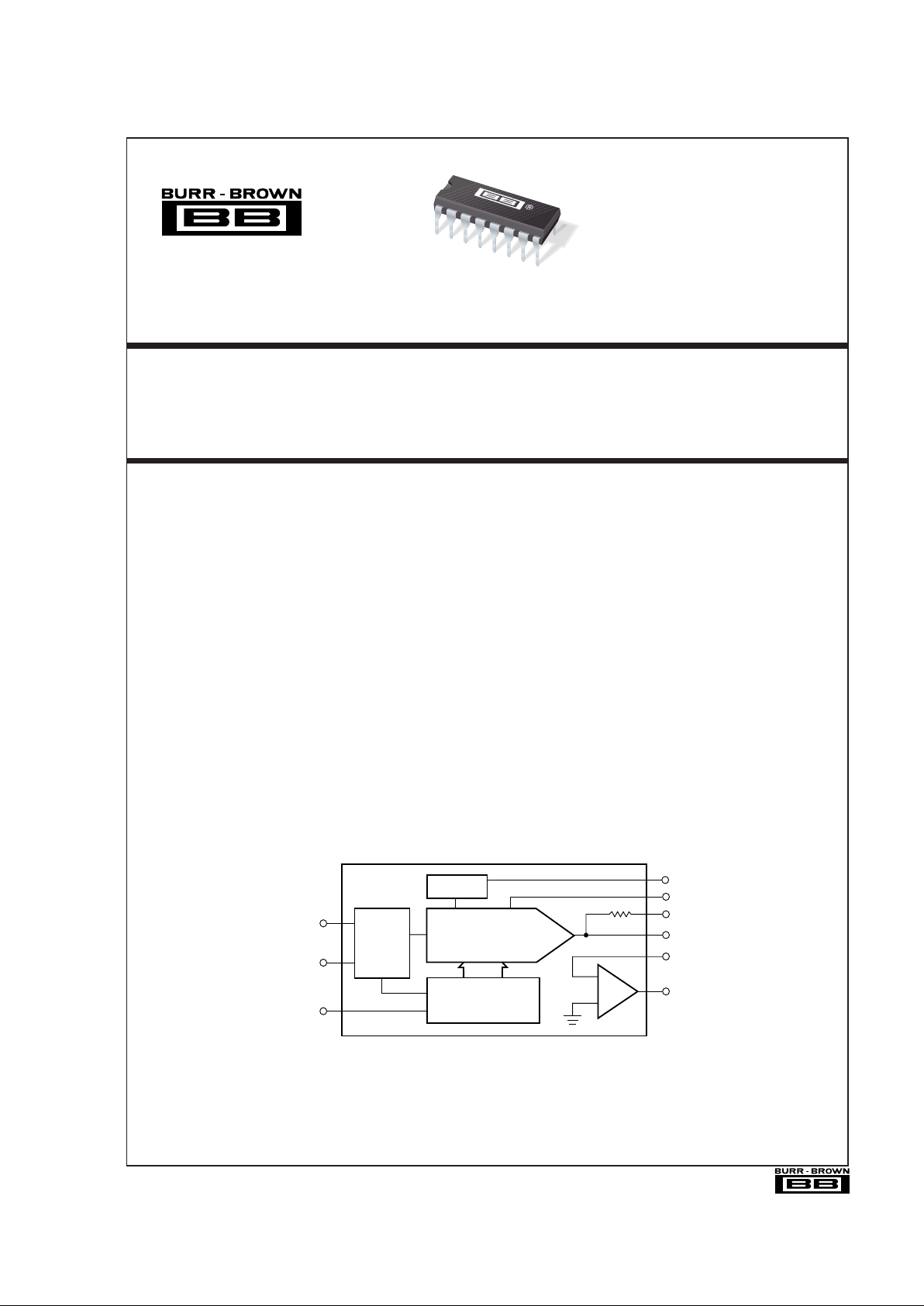
DESCRIPTION
The PCM61P is an 18-bit totally pin compatible performance replacement for the popular 16-bit PCM56P.
With the addition of two extra bits, lower max THD+N
(–92dB; PCM61P-K) can be achieved in audio applications already using the PCM56P. The PCM61P is
complete with internal reference and output op amp and
requires no external parts to function as an 18-bit DAC.
The PCM61P is capable of an 8-times oversampling
rate (single channel) and meets all of its specifications
without an external output deglitcher.
The PCM61P comes in a small, reliable 16-pin plastic
DIP package that has passed operating life tests under
simultaneous high temperature, high humidity and high
pressure testing.
FEATURES
● 18-BIT MONOLITHIC AUDIO D/A
CONVERTER
● LOW MAX THD + N: –92dB Without
External Adjust
● 100% PIN COMPATIBLE WITH INDUSTRY
STD 16-BIT PCM56P
● LOW GLITCH OUTPUT OF
±3V OR ±1mA
● CAPABLE OF 8X OVERSAMPLING RATE
IN V
OUT
MODE
● COMPLETE WITH INTERNAL REFERENCE
AND OUTPUT OP AMP
● RELIABLE PLASTIC 16-PIN DIP PACKAGE
MSB Adj
Ref
R
Serial-To-Parallel
Shift Register
18-Bit
DAC
Control
Logic
VREF
Clock
Data
Latch Enable
F
+
_
SJ
OUT
I
OUT
I
OUT
V
®
International Airport Industrial Park • Mailing Address: PO Box 11400, Tucson, AZ 85734 • Street Address: 6730 S. Tucson Blvd., Tucson, AZ 85706 • Tel: (520) 746-1111 • Twx: 910-952-1111
Internet: http://www.burr-brown.com/ • FAXLine: (800) 548-6133 (US/Canada Only) • Cable: BBRCORP • Telex: 066-6491 • FAX: (520) 889-1510 • Immediate Product Info: (800) 548-6132
PCM61P
Page 2
®
PCM61P
2
SPECIFICATIONS
ELECTRICAL
All specifications at 25°C, and +VCC = +5V, unless otherwise noted.
NOTES: (1) Binary Two’s Complement coding. (2) Ratio of (Distortion
RMS
+ Noise
RMS
)/Signal
RMS
. (3) D/A converter output frequency/signal level. (4) D/A converter
sample frequency (4 x 44.1kHz; 4 times oversampling). (5) Bipolar zero, using A-weighted filter. (6) This is the combined drift error due to gain, offset, and linearity over
temperature. (7) All positive and all negative supply pins must be tied together respectively.
PCM61P-P, J-P, K
PARAMETER CONDITIONS MIN TYP MAX UNITS
RESOLUTION 18 Bits
DYNAMIC RANGE 108 dB
DIGITAL INPUT
Logic Family TTL/CMOS Compatible
Logic Level: V
IH
+2.4 +V
L
V
V
IL
0 +0.8 V
I
IH
VIH = +2.7V +1 µA
I
IL
VIL = +0.4V –50 µA
Data Format Serial BTC
(1)
Input Clock Frequency 16.9 MHz
DYNAMIC CHARACTERISTICS
Total Harmonic Distortion + N
(2)
Without MSB Adjustments
PCM61P
f = 991Hz (0dB)
(3)
fS = 176.4kHz
(4)
–88 –82 dB
f = 991Hz (–20dB) f
S
= 176.4kHz –74 –68 dB
f = 991Hz (–60dB) f
S
= 176.4kHz –34 –28 dB
PCM61P-J
f = 991Hz (0dB) f
S
= 176.4kHz –94 –88 dB
f = 991Hz (–20dB) f
S
= 176.4kHz –76 –74 dB
f = 991Hz (–60dB) f
S
= 176.4kHz –36 –34 dB
PCM61P-K
f = 991Hz (0dB) f
S
= 176.4kHz –98 –92 dB
f = 991Hz (–20dB) f
S
= 176.4kHz –80 –74 dB
f = 991Hz (–60dB) f
S
= 176.4kHz –40 –34 dB
IDLE CHANNEL SNR 20Hz to 20kHz at BPZ
(5)
112 dB
TRANSFER CHARACTERISTICS
ACCURACY
Gain Error ±2 %FSR
Bipolar Zero Error ±30 mV
Differential Linearity Error ±0.001 %FSR
Total Drift
(6)
0°C to 70°C ±25 ppm of FSR/°C
Bipolar Zero Drift 0°C to 70°C ±4 ppm of FSR/°C
Warm-up Time 1 Minute
MONOTONICITY 16 Bits
ANALOG OUTPUT
Voltage: Output Range ±3V
Output Current ±2mA
Output Impedance 0.1 Ω
Current: Output Range ±30% ±1mA
Output Impedance ±30% 1.2 kΩ
SETTLING TIME To ±0.006% of FSR
Voltage: 6V Step 1.5 µs
1 LSB 1.0 µs
Slew Rate 12 V/µs
Current: 1mA Step 10Ω to 100Ω Load 250 ns
1mA Step 1kΩ Load 350 ns
Glitch Energy Meets all THD+N specs without external deglitching
POWER SUPPLY REQUIREMENTS
(7)
±VCC Supply Voltage ±4.75 ±5 ±13.2 V
Supply Current: +I
CC
+VCC = +5V +10 +17 mA
+I
CC
+VCC = +12V +12 mA
–I
CC
–VCC = –5V –25 –35 mA
–I
CC
–VCC = –12V –27 mA
Power Dissipation ±V
CC
= ±5V 175 260 mW
±V
CC
= ±12V 475 mW
TEMPERATURE RANGE
Specification 0 +70 °C
Operating –30 +70 °C
Storage –60 +100 °C
Page 3
®
PCM61P
3
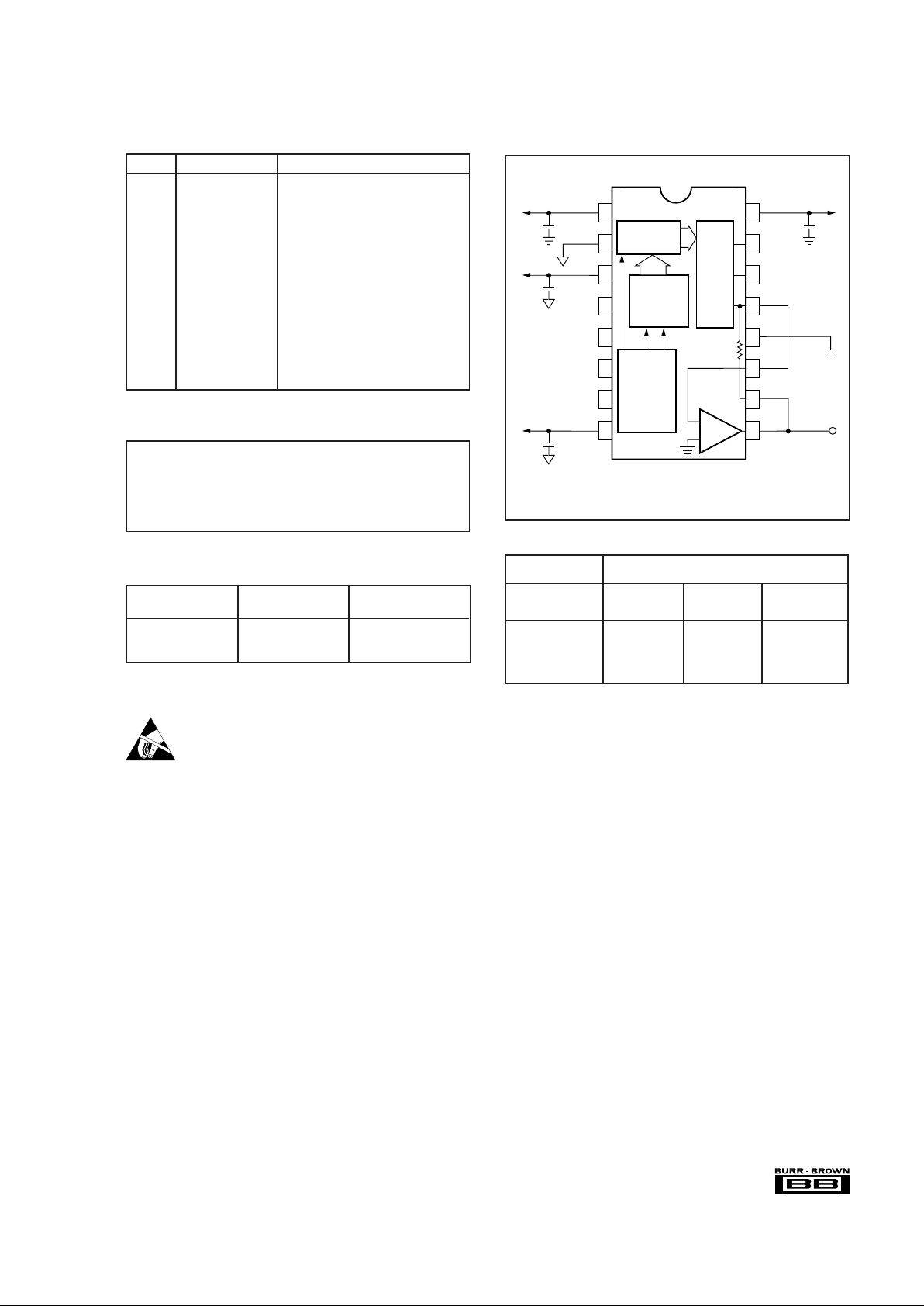
1
2
3
4
5
6
7
8
–V
+V
–V
Logic
Com
+V
I
SJ
RF
V
18-Bit
DAC Latch
Control
Logic
and
Level
Shifting
Circuit
18-Bit Serial
to Parallel
Conversion
–
+
–5V
1µF
S
L
L
+5V
1µF
–5V
1µF
18-Bit
I
DAC
OUT
S
+5V
1µF
(1)
(1)
OUT
OUT
(±3V)
Analog
Common
16
15
14
13
12
11
10
9
Analog
Output
Trim
MSB Adjust
NC
CLK
LE
Data
NOTE: (1) MSB error (Bipolar Zero differential linearity error) can be
adjusted to zero using the external circuit shown in Figure 4.
CONNECTION DIAGRAM
The information provided herein is believed to be reliable; however, BURR-BROWN assumes no responsibility for inaccuracies or omissions. BURR-BROWN assumes
no responsibility for the use of this information, and all use of such information shall be entirely at the user’s own risk. Prices and specifications are subject to change
without notice. No patent rights or licenses to any of the circuits described herein are implied or granted to any third party. BURR-BROWN does not authorize or warrant
any BURR-BROWN product for use in life support devices and/or systems.
DIGITAL INPUT ANALOG OUTPUT
Binary Two’s Voltage (V) Current (mA)
Complement (BTC) DAC Output V
OUT
Mode I
OUT
Mode
1FFFF Hex +FS –0.99999237 +2.99997711
00000 Hex BPZ 0.00000000 0.00000000
3FFFF Hex BPZ – 1LSB +0.00000763 –0.00002289
20000 Hex –FS +1.00000000 –3.00000000
TABLE I. PCM61P Input/Output Relationships.
PIN FUNCTION DESCRIPTION
1–V
S
Analog Negative Supply
2 LOG COM Logic Common
3+V
L
Logic Positive Supply
4 NC No Connection
5 CLK Clock Input
6 LE Latch Enable Input
7 DATA Serial Data Input
8–V
L
Logic Negative Supply
9V
OUT
Voltage Output
10 RF Feedback Resistance
11 SJ Summing Junction
12 ANA COM Analog Common
13 I
OUT
Current Output
14 MSB ADJ MSB Adjustment Terminal
15 TRIM MSB Trim-pot Terminal
16 +V
S
Analog Positive Supply
PIN ASSIGNMENTS
DC Supply Voltages ......................................................................±16VDC
Input Logic Voltage ............................................................. –1V to V
S
/+V
L
Power Dissipation .......................................................................... 850mW
Operating Temperature Range ......................................... –25°C to +70°C
Storage Temperature Range .......................................... –60°C to +100°C
Lead Temperature (soldering, 10s)............................................... +300°C
ABSOLUTE MAXIMUM RATINGS
PACKAGE INFORMATION
PACKAGE DRAWING
PRODUCT PACKAGE NUMBER
(1)
PCM61P-P 16-Pin Plastic DIP 180
PCM61P-J 16-Pin Plastic DIP 180
PCM61P-K 16-Pin Plastic DIP 180
NOTE: (1) For detailed drawing and dimension table, please see end of data
sheet, or Appendix C of Burr-Brown IC Data Book.
ELECTROSTATIC
DISCHARGE SENSITIVITY
This integrated circuit can be damaged by ESD. Burr-Brown
recommends that all integrated circuits be handled with
appropriate precautions. Failure to observe proper handling
and installation procedures can cause damage.
ESD damage can range from subtle performance degradation
to complete device failure. Precision integrated circuits may
be more susceptible to damage because very small parametric
changes could cause the device not to meet its published
specifications.
Page 4

®
PCM61P
4
MSB ERROR ADJUSTMENT PROCEDURE
(OPTIONAL)
The MSB error of the PCM61P can be adjusted to make the
differential linearity error (DLE) at BPZ essentially zero. This
is important when the signal output levels are very low,
because zero crossing noise (DLE at BPZ) becomes very
significant when compared to the small code changes occurring in the LSB portion of the converter.
To statically adjust DLE at BPZ, refer to the circuit shown in
Figure 3 or the PCM61P connection diagram.
Differential linearity error at bipolar zero and THD are guaranteed to meet data sheet specifications without any external
adjustment. However, a provision has been made for an
optional adjustment of the MSB linearity point, which makes
it possible to eliminate DLE error at BPZ. Two procedures are
given to allow either static or dynamic adjustment. The
dynamic procedure is preferred because of the difficulty
associated with the static method (accurately measuring 16bit LSB steps).
After allowing ample warm-up time (5-10 minutes) to assure
stable operation of the PCM61P, select input code 3FFFF
hexadecimal (all bits on except the MSB). Measure the output
voltage using a 6-1/2 digit voltmeter and record it. Change the
digital input code to 00000 hexadecimal (all bits off except the
MSB). Adjust the 100kΩ potentiometer to make the output
read 22.9µV more than the voltage reading of the previous
code (a 1LSB step = 22.9µV). A much simpler method is to
dynamically adjust the DLE at BPZ. Assuming the device has
been installed in a digital audio application circuit, send the
appropriate digital input to produce a –60dB level sinusoidal
output, then adjust the 100kΩ potentiometer until a minimum
level of distortion is observed.
Data
Input
> One Clock Cycle > One Clock Cycle
LSB
MSB
>25ns
>25ns >25ns
>60ns
>5ns
>15ns
Clock
Input
Latch
Enable
>15ns >15ns
FIGURE 2. PCM61P Setup and Hold Timing Diagram.
NOTES: (1) If clock is stopped between input of 18-bit data words, latch enable (LE) must remain low until after the first clock of the next 18-bit data word stream.
(2) Data format is binary two‘s complement (BTC). Individual data bits are clocked in on the corresponding positive clock edge. (3) Latch enable (LE) must remain
low at least one clock cycle after going negative. (4) Latch enable (LE) must be high for at least one clock cycle before going negative.
FIGURE 1. PCM61P Timing Diagram.
MAXIMUM CLOCK RATE
The maximum clock rate of 16.9MHz for the PCM61P is
derived by multiplying the standard audio sample rate of
44.1kHz times sixteen (16 x oversampling) times the standard
audio word bit length of 24 (44.1kHz x 16 x 24 = 16.9MHz).
Note that this clock rate accommodates a 24-bit word length,
even though only 18 bits are actually being used.
100k
Trim 15
Ω
MSB Ad
j
ust 14
1 –V
S
200kΩ470kΩ
FIGURE 3. MSB Adjust Circuit.
1
MSB
23
4 1011121314151617
18
LSB
1
P16 (Clock)
P18 (Data)
P17 (Latch Enable)
 Loading...