

Page 1
®
1 PCM1800
49%
FPO
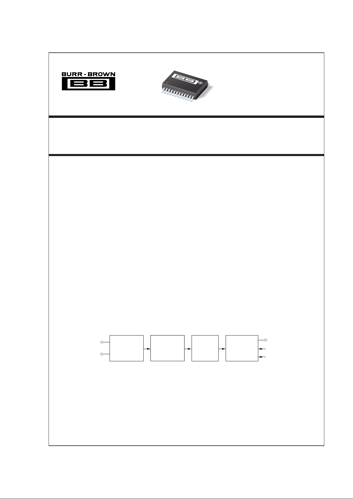
PCM1800
®
FEATURES
● DUAL 20-BIT MONOLITHIC ∆Σ ADC
● SINGLE-ENDED VOLTAGE INPUT
● 64X OVERSAMPLING DECIMATION FILTER:
Passband Ripple:
±0.05dB
Stopband Attenuation: –65dB
● HIGH PERFORMANCE:
THD+N: -88dB (typ)
SNR: 95dB (typ)
Dynamic Range: 95dB (typ)
Internal High Pass Filter
● PCM AUDIO INTERFACE:
Master/Slave Modes
4 Data Formats
● SAMPLING RATE: 32kHz, 44.1kHz, 48kHz
● SYSTEM CLOCK: 256f
S
, 384fS, or 512f
S
● SINGLE +5V POWER SUPPLY
● SMALL 24-PIN SSOP PACKAGE
DESCRIPTION
PCM1800 is a low cost, single chip stereo analog-todigital converter with single-ended analog voltage
inputs. The PCM1800 uses a delta-sigma modulator
with 64X oversampling, including a digital decimation filter and serial interface which supports both
Master and Slave Modes and four data formats.
PCM1800 is suitable for a wide variety of cost-sensitive consumer applications where high performance is
required.
PCM1800 is fabricated on a highly advanced CMOS
process.
© 1997 Burr-Brown Corporation PDS-1387 Printed in U.S.A. August, 1997
International Airport Industrial Park • Mailing Address: PO Box 11400, Tucson, AZ 85734 • Street Address: 6730 S. Tucson Blvd., Tucson, AZ 85706 • Tel: (520) 746-1111 • Twx: 910-952-1111
Internet: http://www.burr-brown.com/ • FAXLine: (800) 548-6133 (US/Canada Only) • Cable: BBRCORP • Telex: 066-6491 • FAX: (520) 889-1510 • Immediate Product Info: (800) 548-6132
Single-Ended Analog Input 20-Bit Stereo
ANALOG-TO-DIGITAL CONVERTER
PCM1800
Analog Input (L)
Analog Input (R)
Analog Front-End
Delta-Sigma
Modulator
Decimation
Digital
Filter
Serial Interface
and
Format Control
Digital Output
Mode/Format Control
System Clock
Page 2
®
2
PCM1800
SPECIFICATIONS
All specifications at +25°C, +VDD = +V
CC
= +5V, fS = 44.1kHz, and 20-bit input data, SYSCLK = 384fS, unless otherwise noted.
PCM1800E
PARAMETER CONDITIONS MIN TYP MAX UNITS
RESOLUTION 20 Bits
DIGITAL INPUT/OUTPUT
Input Logic Level:
V
IH
(1)
2.0 V
V
IL
(1)
0.8 V
Input Logic Current:
I
IN
(2)
±1 µA
I
IN
(3)
+100 µA
Output Logic Level:
V
OH
(4)
IOH = –1.6mA 4.5 V
V
OL
(4)
IOL = +3.2mA 0.5 V
Sampling Frequency 32 44.1 48 kHz
System Clock Frequency 256f
S
8.1920 11.2896 12.2880 MHz
384f
S
12.2880 16.9344 18.4320 MHz
512f
S
16.3840 22.5792 24.5760 MHz
DC ACCURACY
Gain Mismatch Channel-to-Channel ±1.0 ±2.5 % of FSR
Gain Error ±2.0 ±5.0 % of FSR
Gain Drift ±20
ppm of FSR/°C
Bipolar Zero Error High Pass Filter Bypass ±2.0 % of FSR
Bipolar Zero Drift High Pass Filter Bypass ±20
ppm of FSR/°C
DYNAMIC PERFORMANCE
(5)
THD+N at FS (–0.5dB) –88 –80 dB
THD+N at –60dB –92 dB
Dynamic Range EIAJ, A-weighted 90 95 dB
Signal-To-Noise Ratio EIAJ, A-weighted 90 95 dB
Channel Separation 88 93 dB
DYNAMIC PERFORMANCE
(5)
Dynamic Range 16-Bit, A-weighted 94 dB
Signal-To-Noise Ratio 16-Bit, A-weighted 94 dB
Channel Separation 16-Bit 92 dB
ANALOG OUTPUT
Input Range FS (V
IN
= 0dB) 2.828 Vp-p
Center Voltage 2.1 V
Input Impedance 30 kΩ
Anti-Aliasing Filter Frequency Response C
EXT
= 470pF, –3dB 170 kHz
DIGITAL FILTER PERFORMANCE
Passband 0.454f
S
Hz
Stopband 0.583f
S
Hz
Passband Ripple ±0.05 dB
Stopband Attenuation –65 dB
Delay Time (Latency) 17.4/f
S
sec
High Pass Frequency Response –3dB 0.019f
S
mHz
POWER SUPPLY REQUIREMENTS
Voltage Range +V
CC
+4.5 +5.0 +5.5 VDC
+V
DD
+4.5 +5.0 +5.5 VDC
Supply Current
(6)
+VCC = +VDD = +5V 18 25 mA
Power Dissipation +V
CC
= +VDD = +5V 90 125 mW
TEMPERATURE RANGE
Operation –25 +85 °C
Storage –55 +125 °C
Thermal Resistance,
θ
JA
100 °C/W
NOTES: (1) Pins 6, 7, 8, 9, 10, 11, 16 and 12, 13, 14: RSTB, BYPAS, FMT0, FMT1, MODE0, MODE1, SYSCLK, and FSYNC, LRCK, BCK under Slave Mode.
(2) Pins 16 and 12, 13, 14: SYSCLK and FSYNC, LRCK, BCK under Slave Mode (Schmitt Trigger input). (3) Pins 6, 7, 8, 9, 10, 11: RSTB, BYPAS, FMT0,
FMT1, MODE0, MODE1 (Schmitt Trigger input, with 100kΩ typical pull-down resistor). (4) Pins 15 and 12, 13, 14: DOUT and FSYNC, LRCK, BCK under Master
Mode. (5) f
IN
= 1kHz, using Audio Precisions System II, rms Mode with 20kHz LPF and 400Hz HPF in calculation. (6) No load on DOUT (pin 15) in the Slave
Mode.
Page 3
®
3 PCM1800
VINL
V
REF
1
REFCOM
V
REF
2
V
IN
R
RSTB
BYPAS
FMT0
FMT1
MODE0
MODE1
FSYNC
AGND
V
CC
CINPL
C
IN
NL
C
IN
PR
C
IN
NR
V
DD
DGND
SYSCLK
DOUT
BCK
LRCK
1
2
3
4
5
6
7
8
9
10
11
12
24
23
22
21
20
19
18
17
16
15
14
13
PCM1800
PIN CONFIGURATION
The information provided herein is believed to be reliable; however, BURR-BROWN assumes no responsibility for inaccuracies or omissions. BURR-BROWN assumes no
responsibility for the use of this information, and all use of such information shall be entirely at the user’s own risk. Prices and specifications are subject to change without notice.
No patent rights or licenses to any of the circuits described herein are implied or granted to any third party. BURR-BROWN does not authorize or warrant any BURR-BROWN
product for use in life support devices and/or systems.
PIN NAME I/O DESCRIPTION
1V
IN
L IN Analog Input, Lch
2V
REF
1 — Reference 1 Decoupling Capacitor
3 REFCOM — Reference Decoupling Common
4V
REF
2 — Reference 2 Decoupling Capacitor
5V
IN
R IN Input Reference, Rch
6 RSTB IN Reset Input, Active LOW
(1)
7 BYPAS IN High Pass Filter Bypass Control
(1)
8 FMT0 IN Audio Data Format 0
(1)
9 FMT1 IN Audio Data Format 1
(1)
10 MODE0 IN Master/Slave Mode Selection 0
(1)
11 MODE1 IN Master/Slave Mode Selection 1
(1)
12 FSYNC IN/OUT Frame Synchronization
13 LRCK IN/OUT Sampling Clock Input/Output (f
S
)
14 BCK IN/OUT Bit Clock Input/Output
15 DOUT OUT Audio Data Output
16 SYSCLK IN System Clock Input, 256f
S
, 384fS, or 512f
S
17 DGND — Digital Ground
18 V
DD
— Digital Power Supply
19 C
IN
NR — Anti-alias Filter Capacitor (–), Rch
20 C
IN
PR — Anti-alias Filter Capacitor (+), Rch
21 C
IN
NL — Anti-alias Filter Capacitor (–), Lch
22 C
IN
PL — Anti-alias Filter Capacitor (+), Lch
23 V
CC
— Analog Power Supply
24 AGND — Analog Ground
NOTE: (1) With 100kΩ typical pull-down resistor.
PIN ASSIGNMENTS
Top View SSOP
Supply Voltage: +V
DD, +VCC
......................................................................................
+6.5V
Supply Voltage Differences............................................................... ±0.1V
GND Voltage Differences.................................................................. ±0.1V
Digital Input Voltage ................................................. –0.3V to (V
DD
+ 0.3V)
Analog Input Voltage................................................ –0.3V to (V
CC
+ 0.3V)
Input Current (any pin except supplies) .......................................... ±10mA
Power Dissipation .......................................................................... 300mW
Operating Temperature Range ......................................... –25°C to +85°C
Storage Temperature ...................................................... –55°C to +125°C
Lead Temperature (soldering, 5s).................................................. +260°C
(reflow, 10s) ..................................................... +235°C
ABSOLUTE MAXIMUM RATINGS
PACKAGE DRAWING
PRODUCT PACKAGE NUMBER
(1)
PCM1800E 24-Pin SSOP 338
NOTE: (1) For detailed drawing and dimension table, please see end of data
sheet, or Appendix C of Burr-Brown IC Data Book.
PACKAGE INFORMATION
ELECTROSTATIC
DISCHARGE SENSITIVITY
This integrated circuit can be damaged by ESD. Burr-Brown
recommends that all integrated circuits be handled with
appropriate precautions. Failure to observe proper handling
and installation procedures can cause damage.
ESD damage can range from subtle performance degradation
to complete device failure. Precision integrated circuits may
be more susceptible to damage because very small parametric
changes could cause the device not to meet its published
specifications.
Page 4
®
4
PCM1800
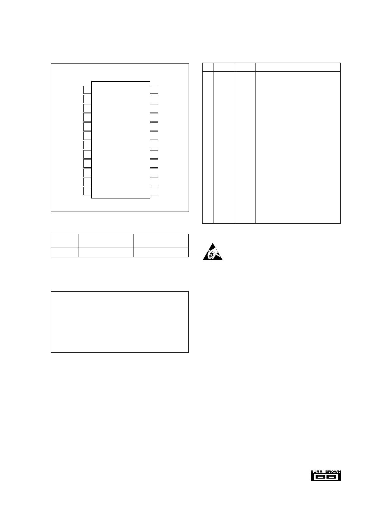
BLOCK DIAGRAM
ANALOG FRONT-END (Single-Channel)
30kΩ
1kΩ
C
EXT
470pF
2122
VINL
V
REF
2
C
IN
PL CINNL
1
4
3
2
1kΩ
Delta-Sigma
Modulator
(+)
(–)
V
REF
REFCOM
V
REF
1
+
+
1.0µF
4.7µF
+
4.7µF
Clock/Timing Control
Reset/Power Control
BYPAS
V
CC
V
DD
AGND
Reference
Mode/Format
Control
Interface
FMT0
FMT1
SYSCLK
RSTB
MODE0
MODE1
Serial Data
Interface
DOUT
BCK
LRCK
FSYNC
C
IN
PL
C
IN
NL
V
IN
L
V
REF
1
V
REF
2
V
IN
R
C
IN
NR
C
IN
PR
Power Supply
DGND
(–)
(+)
x1/64
Decimation
and
High Pass Filter
5th-Order
Delta-Sigma
Modulator
5th-Order
Delta-Sigma
Modulator
ADC
(+)
(–)
Single-End/
Differential
Converter
Single-End/
Differential
Converter
REFCOM
Page 5
®
5 PCM1800
TYPICAL PERFORMANCE CURVES
At TA = +25°C, +VDD = +V
CC
= +5V, fS = 44.1kHz, and 20-bit input data, SYSCLK = 384fS, unless otherwise noted.
THD+N vs POWER SUPPLY
Supply Voltage
(V)
THD+N at –0.5dB (%)
0.010
0.008
0.006
0.004
0.002
4.5 4.75 5.0 5.25 5.5
THD+N at –60dB (%)
4.0
3.0
2.0
1.0
0
–60dB
–0.5dB
SNR and DYNAMIC RANGE vs POWER SUPPLY
Supply Voltage (V)
SNR (dB)
98
96
94
92
90
4.5 4.75 5.0 5.25 5.50
Dynamic Range (dB)
98
96
94
92
90
SNR
Dynamic Range
THD+N vs SYSTEM CLOCK
and SAMPLING FREQUENCY
System Clock
THD+N at –0.5dB (%)
0.010
0.008
0.006
0.004
0.002
256f
S
384f
S
512f
S
THD+N at –60dB (%)
4.0
3.0
2.0
1.0
0
48kHz
44.1kHz
32kHz
48kHz
32kHz
–60dB
–0.5dB
44.1kHz
THD+N vs OUTPUT DATA RESOLUTION
Resolution
THD+N at –0.5dB (%)
THD+N at –60dB (%)
0.010
0.008
0.006
0.004
0.002
16-Bit 20-Bit
4.0
3.0
2.0
1.0
0
–0.5dB
–60dB
THD+N vs TEMPERATURE
Temperature (°C)
THD+N at –0.5dB (%)
0.010
0.008
0.006
0.004
0.002
–25 0 25 50 75 85 100
THD+N at –60dB (%)
4.0
3.0
2.0
1.0
0
–60dB
–0.5dB
SNR, DYNAMIC RANGE vs TEMPERATURE
Temperature (°C)
SNR (dB)
98
96
94
92
90
–25 0 25 50 75 85 100
Dynamic Range (dB)
4.0
3.0
2.0
1.0
0
SNR
Dynamic Range
Page 6

®
6
PCM1800
–60dBFS FFT
Frequency (kHz)
Amplitude (dB)
0
–10
–20
–30
–40
–50
–60
–70
–80
–90
–100
–110
–120
–130
–140
–150
–160
0462 8 10 12 14 16 18 20
TYPICAL PERFORMANCE CURVES (CONT)
At TA = +25°C, +VDD = +V
CC
= +5V, fS = 44.1kHz, and 20-bit input data, SYSCLK = 384fS, unless otherwise noted.
THD+N vs AMPLITUDE
Amplitude (dBr)
THD+N (dB)
0
–5
–10
–15
–20
–25
–30
–35
–40
–45
–50
–55
–60
–65
–70
–75
–80
–85
–90
–95
–100
–100 –90 –80 –60–70 –50 –30–40 –20 –10 0
THD+N vs FREQUENCY
Frequency (Hz)
THD+N (dB)
–80
–81
–82
–83
–84
–85
–86
–87
–88
–89
–90
–91
–92
–93
–94
–95
–96
–97
–98
–99
–100
20 50 100 500200 1k 2k 5k 10k 20k
Page 7

®
7 PCM1800
TYPICAL PERFORMANCE CURVES
DIGITAL FILTER
STOPBAND ATTENUATION CHARACTERISTICS
Normalized Frequency (x f
S
Hz)
Amplitude (dB)
0
–20
–40
–60
–80
–100
0.25 0.50 0.75 1.000
PASSBAND RIPPLE CHARACTERISTICS
Normalized Frequency (x f
S
Hz)
Amplitude (dB)
0.2
0.0
–0.2
–0.4
–0.6
–0.8
–1.0
0.1 0.30.2 0.4 0.50
TRANSIENT BAND CHARACTERISTICS
Normalized Frequency (x f
S
Hz)
Amplitude (dB)
0
–1
–2
–3
–4
–5
–6
–7
–8
–9
–10
0.46 0.47 0.48 0.49 0.50 0.51 0.52 0.53 0.54 0.550.45
OVERALL CHARACTERISTICS
Normalized Frequency (x f
S
Hz)
Amplitude (dB)
0
–50
–100
–150
–200
81624320
HIGH PASS FILTER RESPONSE
Normalized Frequency (x f
S
/1000Hz)
Amplitude (dB)
0
–10
–20
–30
–40
–50
–60
–70
–80
–90
–100
0.10.05 0.20.15 0.30.25 0.4-0.350
HIGH PASS FILTER RESPONSE
Normalized Frequency (x f
S
/1000Hz)
Amplitude (dB)
0.2
0.0
–0.2
–0.4
–0.6
–0.8
–1.0
1.00.5 2.01.5 3.02.5 4.03.50
HIGH PASS FILTER
Page 8

®
8
PCM1800
TYPICAL PERFORMANCE CURVES
ANTI-ALIASING FILTER
ANTI-ALIASING FILTER OVERALL
FREQUENCY RESPONSE (C
EXT
= 470pF, 1000pF)
Frequency (Hz)
Amplitude (dB)
0
–10
–20
–30
–40
–50
10 100 1k 10k 100k 1M 10M0
470pF
1000pF
ANTI-ALIASING FILTER PASSBAND
FREQUENCY RESPONSE (C
EXT
= 470pF, 1000pF)
Frequency (Hz)
Amplitude (dB)
0.2
0.0
–0.2
–0.4
–0.6
–0.8
–0.1
10 100 1k 10k 100k0
470pF
1000pF
Page 9

®
9 PCM1800
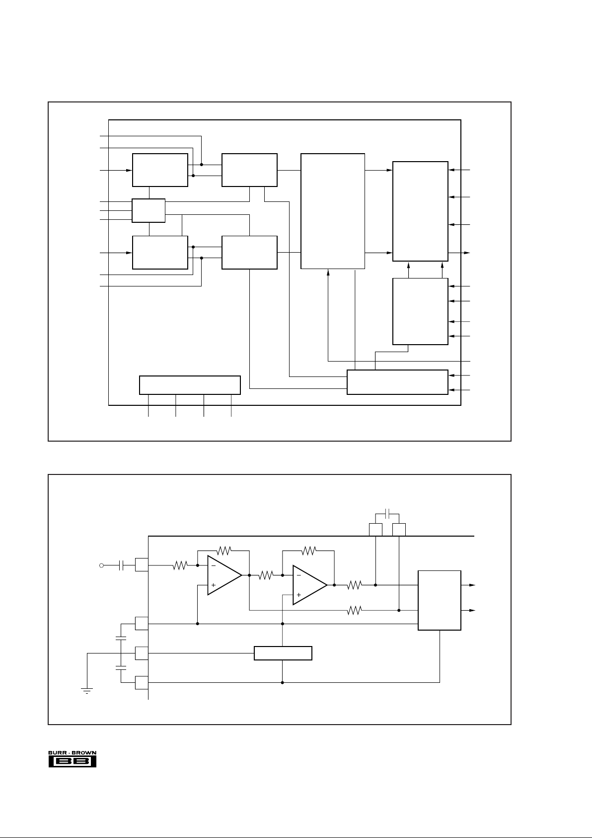
THEORY OF OPERATION
PCM1800 consists of a bandgap reference, two channels of
a single-to-differential converter, a fully differential 5thorder delta-sigma modulator, a decimation filter (including
digital high pass), and a serial interface circuit. The Block
Diagram illustrates the total architecture of PCM1800, the
Analog Front-End diagram illustrates the architecture of the
single-to-differential converter, and the anti-aliasing filter is
illustrated in the Block Diagram. Figure 1 illustrates the
architecture of the 5th-order delta-sigma modulator and
transfer functions.
An internal high precision reference with two external capacitors provides all reference voltages which are required
by the converter, and defines the full-scale voltage range of
both channels. The internal single-to-differential voltage
converter saves the design, space and extra parts needed for
external circuitry required by many delta-sigma converters.
The internal full differential architecture provides a wide
dynamic range and excellent power supply rejection performance.
The input signal is sampled at 64X oversampling rate,
eliminating the need for a sample-and-hold circuit, and
simplifying anti-alias filtering requirements. The 5th-order
delta-sigma noise shaper consists of five integrators which
use a switched-capacitor topology, a comparator and a
feedback loop consisting of a 1-bit DAC. The delta-sigma
modulator shapes the quantization noise, shifting it out of
the audio band in the frequency domain. The high order of
the modulator enables it to randomize the modulator outputs, reducing idle tone levels.
The 64f
S
, 1-bit stream from the modulator is converted to
1fS, 20-bit digital data by the decimation filter, which also
acts as a low pass filter to remove the shaped quantization
noise. The DC components are removed by a high pass filter,
and the filtered output is converted to time-multiplexed
serial signals through a serial interface which provides
flexible serial formats and Master/Slave Modes.
SYSTEM CLOCK
The system clock for PCM1800 must be either 256f
S
, 384fS,
or 512fS, where fS is the audio sampling frequency. The
system clock must be supplied on SYSCLK (pin 16).
PCM1800 also has a system clock detection circuit which
automatically senses if the system clock is operating at
256f
S
, 384fS, or 512fS.
When 384f
S
and 512fS system clock is in Slave Mode, the
system clock is divided into 256fS automatically. The 256f
S
clock is used to operate the digital filter and the modulator.
Table I lists the relationship of typical sampling frequencies
and system clock frequencies. Figure 2 illustrates the system
clock timing.
FIGURE 1. Simplified Diagram of the PCM1800 5th-Order Delta-Sigma Modulator.
FIGURE 2. System Clock Timing.
+
+
–
+
+
+
5th SW-CAP
Integrator
4th SW-CAP
Integrator
3rd SW-CAP
Integrator
2nd SW-CAP
Integrator
1st SW-CAP
Integrator
+
+
+
+
–
+
+
–
1-Bit
DAC
H(z)
Qn(z)
Analog In
X(z)
Digital Out
Y(z)
Y(z) = STF(z) • X(z) + NTF(z) • Qn(z)
Signal Transfer Function
Noise Transfer Function
STF(z) = H(z)/[1 + H(z)]
NTF(z) = 1/[1 + H(z)]
Comparator
SAMPLING RATE FREQUENCY SYSTEM CLOCK FREQUENCY
(kHz) (MHz)
256f
S
384f
S
512f
S
32 8.1920 12.2880 16.3840
44.1 11.2896 16.9340 22.5792
48 12.2880 18.4320 24.5760
TABLE I. System Clock Frequencies.
t
CLKIH
System Clock Pulse Width High t
CLKIH
12ns (min)
System Clock Pulse Width Low t
CLKIL
12ns (min)
t
CLKIL
SYSCLK
2.0V
0.8V
Page 10

®
10
PCM1800
RESET
PCM1800 has both an internal power-on reset circuit and an
external forced reset (RSTB, pin 6). The internal power-on
reset initializes (resets) when the supply voltage (V
CC/VDD
)
exceeds 4.0V (typ). To initiate the reset sequence externally,
apply a logic level LOW to the RSTB pin.
The RSTB pin is terminated by an internal pull-down
resistor. If the RSTB pin is unconnected, the ADC will
remain in the reset state. During V
CC/VDD
< 4.0V (typ),
RSTB = LOW and 1024 system clock periods after VCC/
VDD 4.0V and RSTB = HIGH. The PCM1800 stays in the
reset state and the digital output is forced to zero. The
digital output is valid after reset state release and 18436f
S
periods. During reset, the logic circuits and the digital
filter stop operating. Figures 3 and 4 illustrate the internal
power-on reset and external reset timing.
SERIAL AUDIO DATA
INTERFACE
The PCM1800 interfaces the audio system through BCK (pin
14), LRCK (pin 13), FSYNC (pin 12) and DOUT (pin 15).
INTERFACE MODE
The PCM1800 supports Master and Slave Modes as interface modes and are selected by MODE1 (pin 11) and
MODE0 (pin 10), as shown in Table II. In case of the Master
Mode, the PCM1800 provides the timing of serial audio data
communications between the PCM1800 and the digital audio processor or external circuit. While in the case of the
Slave Mode, the PCM1800 receives the timing of data
transfer from an external controller.
MODE1 MODE0 INTERFACE MODE
0 0 Slave Mode (256/384/512f
S
)
0 1 Master Mode (512f
S
)
1 0 Master Mode (384f
S
)
1 1 Master Mode (256f
S
)
TABLE II. Interface Modes.
Master Mode
In the Master Mode, BCK, LRCK, and FSYNC are output
pins and are controlled by timing generated in clock circuitry of the PCM1800.
FSYNC is used to designate the valid data from the PCM1800.
The rising edge of FSYNC indicates the starting point of the
converted audio data and the following edge of this signal
indicates the ending points of data. The frequency of this
signal is fixed at 2xLRCK and duty cycle ratio depends on
data bit length. The frequency of BCK is fixed at 64X
LRCK.
Slave Mode
In Slave Mode, BCK, LRCK, and FSYNC are input pins.
FSYNC is used to enable BCK signal, and the PCM1800 can
shift out the converted data when FSYNC is HIGH.
FIGURE 4. RSTB-Pin Reset Timing.
1024 System Clock Periods
Reset
Reset Removal
System Clock
Internal Reset
RSTB-pin
t
RST
t
RST
= 40ns minimum
FIGURE 3. Internal Power-On Reset Timing.
1024 System Clock Periods
Reset
Reset Removal
4.4V
4.0V
3.6V
VCC/V
DD
Internal Reset
System Clock
Page 11

®
11 PCM1800
DATA FORMAT
PCM1800 supports four audio data formats in both Master
and Slave Modes, and are selected by FMT1 (pin 9) and
FMT0 (pin 8), as shown in Table III.
FORMAT # FMT1 FMT0 DATA FORMAT
0 0 0 20-bit, Left-justified
1 0 1 20-bit, I
2
S
2 1 0 16-bit, Right-justified
3 1 1 20-bit, Right-justified
NOTE: FMT1 and FMT0 must be stable at RSTB changing from LOW to
HIGH.
TABLE III. Data Format.
FIGURE 5. Audio Data Format (Slave Mode: FSYNC, LRCK, and BCK are inputs).
L–ch R–ch
FORMAT 0: FMT[1:0] = “00”
20-Bit, MSB-First, Left-Justified
MSB LSB
LRCK
BCK
DOUT
MSB LSB
123 18 19 20 123 18 19 20 1
MSB
L–ch R–ch
L–ch R–ch
LSB
LRCK
BCK
FORMAT 2: FMT[1:0] = “10”
FORMAT 3: FMT[1:0] = “11”
DIN
MSB LSB
16-Bit, MSB-First, Right-Justified
20-Bit, MSB-First, Right-Justified
116
20
23
14 15 16 123 14 15 16
MSB
LSB
LRCK
BCK
DOUT
MSB LSB
123 18 19 20 123 18 19 20
FORMAT 1: FMT[1:0] = “01”
L-ch
R-ch
20-Bit, MSB-First, I
2
S
MSB
LSB
LRCK
FSYNC
BCK
DOUT
MSB LSB
FSYNC
FSYNC
FSYNC
123 18 19 20 123 18 19 20
Page 12

®
12
PCM1800
FIGURE 6. Audio Data Format (Master Mode: FSYNC, LRCK, and BCK are outputs).
L–ch R–ch
FORMAT 0: FMT[1:0] = “00”
20-Bit, MSB-First, Left-Justified
MSB LSB
LRCK
BCK
DOUT
MSB LSB
123 18 19 20 123 18 19 20 1
MSB
L–ch R–ch
L–ch R–ch
LSB
LRCK
BCK
FORMAT 2: FMT[1:0] = “10”
FORMAT 3: FMT[1:0] = “11”
DIN
MSB LSB
16-Bit, MSB-First, Right-Justified
20-Bit, MSB-First, Right-Justified
116
20
23
14 15 16 123 14 15 16
MSB
LSB
LRCK
BCK
DOUT
MSB LSB
123 18 19 20 123 18 19 20
FORMAT 1: FMT[1:0] = “01”
L-ch
R-ch
20-Bit, MSB-First, I
2
S
MSB
LSB
LRCK
FSYNC
BCK
DOUT
MSB LSB
FSYNC
FSYNC
FSYNC
123 18 19 20 123 18 19 20
Page 13

®
13 PCM1800
FIGURE 8. Audio Data Interface Timing (Master Mode: FSYNC, LRCK, and BCK are outputs).
LRCIN
FSYNC 0.5V
DD
0.5V
DD
0.5V
DD
0.5V
DD
BCKIN
DOUT
t
BCKH
t
CKFS
t
FSYP
t
LRCP
t
CKDO
t
LRDO
t
CKLR
t
BCKP
t
BCKL
DESCRIPTION SYMBOL MIN TYP MAX UNITS
BCK Period t
BCKP
300 1/64fS600 ns
BCK Pulsewidth HIGH t
BCKH
150 300 ns
BCK Pulsewidth LOW t
BCKL
150 300 ns
Delay Time BCK Falling Edge to LRCK Valid t
CKLR
–20 40 ns
LRCK Period t
LRCP
20 1/f
S
40 µs
Delay Time BCK Falling Edge to FSYNC Valid t
CKFS
–20 40 ns
FSYNC Period t
FSYP
10 1/2 f
S
40 µs
Delay Time BCK Falling Edge to DOUT Valid t
CKDO
–20 40 ns
Delay Time LRCK Edge to DOUT Valid t
LRDO
–20 40 ns
Rising Time of All Signals t
RISE
20 ns
Falling Time of All SIgnals t
FALL
20 ns
NOTE: Timing measurement reference level is (VIH/VIL)/2. Rising and falling time is measured from 10% to
90% of I/O signals’ swing. Load capacitance of DOUT signal is 20pF.
FIGURE 7. Audio Data Interface Timing (Slave Mode: FSYNC, LRCK, and BCK are inputs).
LRCK
FSYNC 1.4V
1.4V
1.4V
0.5V
DD
BCK
DOUT
t
BCKH
t
FSSU
t
LRCP
t
CKDO
t
LRDO
t
BCKP
t
BCKL
t
LRHD
t
LRSU
t
FSHD
DESCRIPTION SYMBOL MIN TYP MAX UNITS
BCK Period t
BCKP
300 ns
BCK Pulsewidth HIGH t
BCKH
120 ns
BCK Pulsewidth LOW t
BCKL
120 ns
LRCK Set Up Time to BCK Rising Edge t
LRSU
80 ns
LRCK Hold Time to BCK Rising Edge t
LRHD
40 ns
LRCK Period t
LRCP
20 µs
FSYNC Set Up Time to BCK Rising Edge t
FSSU
40 ns
FSYNC Hold Time to BCK Rising Edge t
FSHD
40 ns
Delay Time BCK Falling Edge to DOUT Valid t
CKDO
–20 40 ns
Delay Time LRCK Edge to DOUT Valid t
LRDO
–20 40 ns
Rising Time of All Signals t
RISE
20 ns
Falling Time of All Signals t
FALL
20 ns
NOTE: Timing measurement reference level is (VIH/VIL)/2. Rising and falling time is measured from 10% to
90% of I/O signals’ swing. Load capacitance of DOUT signal is 20pF.
Page 14

®
14
PCM1800
SYNCHRONIZATION WITH
DIGITAL AUDIO SYSTEM
In Slave Mode, PCM1800 operates with LRCK synchronized to the system clock (SYSCLK). PCM1800 does not
require a specific phase relationship between LRCK and
SYSCLK, but does require the synchronization of LRCK
and SYSCLK. If the relationship between LRCK and
SYSCLK changes more than 6 bit clocks (BCK) during one
sample period due to LRCK or SYSCLK jitter, internal
operation of the ADC halts within 1/fS and digital output is
forced into BPZ code until resynchronization between LRCK
and SYSCLK is completed. In case of changes less than 5 bit
clocks (BCK), resynchronization does not occur and above
digital output control and discontinuity does not occur.
ADC DATA OUTPUT AT RESET
Figures 9 and 10 illustrate the ADC digital output when the
reset operation is done and synchronization is lost. During
undefined data, it may generate some noise in the audio signal.
Also, the transition of normal to undefined data and undefined
or zero data to normal makes a discontinuity of data on the
digital output, and may generate some noise in the audio signal.
BOARD DESIGN AND LAYOUT
CONSIDERATIONS
VCC, VDD PINS
The digital and analog power supply lines to the PCM1800
should be bypassed to the corresponding ground pins with
both 0.1µF ceramic and 10µF tantalum capacitors as close to
the pins as possible to maximize the dynamic performance
of the ADC. Although PCM1800 has two power lines to
maximize the potential of dynamic performance, using one
common power supply is recommended to avoid unexpected
power supply problems, such as latch-up or power supply
sequence.
AGND, DGND PINS
To maximize the dynamic performance of the PCM1800,
the analog and digital grounds are not internally connected.
These points should have very low impedance to avoid
digital noise feedback into the analog ground. They should
be connected directly to each other under the parts to reduce
potential noise problems.
FIGURE 9. ADC Output for Power-On Reset and RSTB Control.
FIGURE 10. ADC Output When Synchronization is Lost and for Resynchronization.
Reset Ready/Operation
Internal Reset
DOUT
(1)
Zero Data Normal Data
(2)
18436/f
S
Reset Release
Power ON
RSTB ON
NOTES: (1) In the Master Mode, FSYNC, BCK, and LRCK are outputs similar to DOUT.
(2) The HPF transient response (exponentially attenuationed signal from ±0.2% DC of FSR
with 200ms time constant) appears initially.
Synchronous Asynchronous
Synchronization
Lost
Resynchronization
1/f
S
Synchronous
Normal
Normal
(2 )
Zero Data
32/f
S
Undefined Data
State of
Synchronization
DOUT
(1 )
NOTES: (1) Applies only for Slave Mode—the loss of synchronization never occurs in Master Mode.
(2) The HPF transient response (exponentially attenuationed signal from ±0.2% DC of FSR
with 200ms time constant) appears initially.
Page 15

®
15 PCM1800
FIGURE 11. Typical Circuit Connection.
V
IN
PINS
A 1.0µF tantalum capacitor is recommended as an ACcoupling capacitor which establishes a 5.3Hz cut-off frequency. If a higher full-scale input voltage is required, the
input voltage range can be increased by adding a series
resistor to the V
IN
pins.
V
REF
INPUTS
A 4.7µF tantalum capacitor is recommended between V
REF
1,
V
REF
2, and REFCOM to ensure low source impedance for
the ADC’s references. These capacitors should be located as
close as possible to the V
REF
1 or V
REF
2 pin to reduce
dynamic errors on the ADC’s references. The REFCOM pin
should also be connected directly to AGND under the parts.
C
IN
P and CINN INPUTS
A 470pF to 1000pF film capacitor is recommended between
C
IN
PL and CINNL, CINPR and CINNR to create an antialiasing filter, which will have an 170kHz to 80kHz cut-off
frequency. These capacitors should be located as close as
possible to the CINP and CINN pins to avoid introducing
unexpected noise or dynamic errors into the delta-sigma
modulator.
DOUT, BCK, LRCK, FSYNC PINS
The DOUT, BCK, LRCK and FSYNC pins in Master Mode
have a large load drive capability, but locating the buffer
near the PCM1800 and minimizing the load capacitance is
recommended in order to minimize the digital analog crosstalk
and to maximize dynamic performance potential.
SYSTEM CLOCK
The quality of the system clock can influence dynamic
performance in the PCM1800. The duty cycle, jitter, and
threshold voltage at the system clock input pin must be
carefully managed. When power is supplied to the part, the
system clock, bit clock (BCK), and a word clock (LRCK)
should also be supplied simultaneously. Failure to supply
the audio clocks will result in a power dissipation increase
of up to three times normal dissipation and may degrade
long-term reliability if the maximum power dissipation limit
is exceeded.
RSTB Control
If the capacitance between V
REF
1 and V
REF
2 exceeds 4.7µF,
an external reset control delay time circuit must be used.
1
2
3
4
5
6
7
8
9
10
11
12
24
23
22
21
20
19
18
17
16
15
14
13
SYSCLK
DOUT
BCK
LRCK
/RESET
BYPASS
FORMAT0
FORMAT1
MODE0
MODE1
SYNC
+
4.7µF
+
1.0µF
(2)
Analog
Front-End
Analog
Front-End
Delta-Sigma
Decimation Filter
Digital Audio Interface
Reset
Clock
Audio
Data
Processor
Pin Program
or Control
Line In Left-Channel
+
1.0µF
(2)
Line In Right-Channel
GND
+5V
+
4.7µF
NOTES: (1) Bypass capacitor = 0.1µF ceramic and 10µF tantalum, depending on layout
and power supply. (2) A 1.0µF capacitor gives 5.3Hz (τ = 1µF x 30kΩ) cut-off frequency
of input HPF in normal operation and requires power-on settling time with 60ms time
constant in power on initialization period.
Ref
0.1µF/10µF
(1)
0.1µF/10µF
(1)
+
+
C
EXT
470pF
C
EXT
470pF
 Loading...