

Page 1
1
®
PCM1750
Dual CMOS 18-Bit Monolithic Audio
ANALOG-TO-DIGITAL CONVERTER
DESCRIPTION
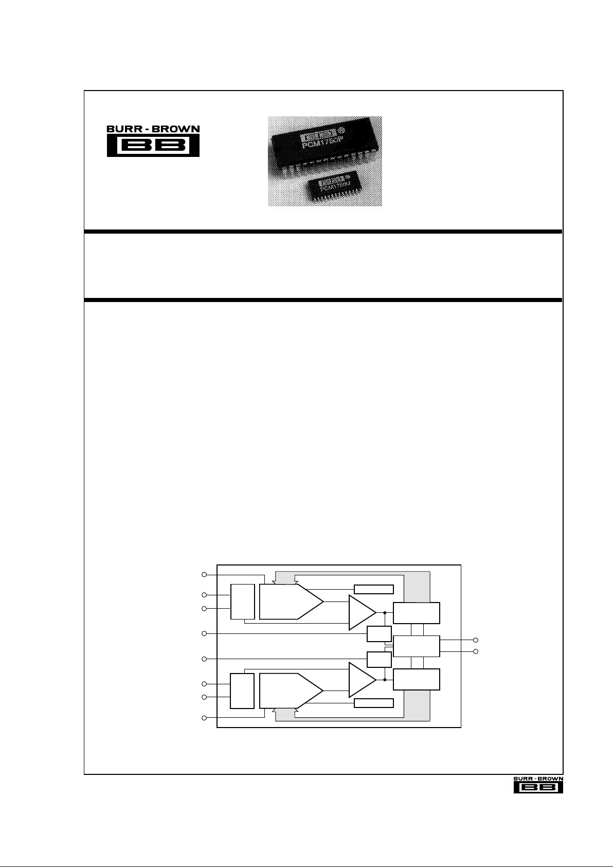
The PCM1750 is a low cost, dual 18-bit CMOS
analog-to-digital converter optimized for dynamic signal applications. The PCM1750 features true co-phased
inputs with an internal sample/hold function for each
channel. The PCM1750 also comes complete with an
internal reference. Total power dissipation is less than
300mW max using ±5V voltage supplies. Low maximum Total Harmonic Distortion + Noise (–88dB max)
is 100% tested. The very fast PCM1750 is capable
of 4X x audio bandwidth oversampling rates on both
input channels simultaneously, providing greater freedom to designers in selecting input anti-aliasing filters.
PCM1750 outputs serial data in a format that is compatible with many digital filter chips and comes packaged in a space saving 28-pin plastic DIP or SOIC.
Offset Adj Right
18-Bit SAR
18-Bit SAR
CDAC
Right
S/H
CDAC
Left
S/H
Reference
V Left
S Left
S Right
Comp
Clock
Convert
Offset Adj Left
MSB Adj Right
MSB Adj Left
V Right
IN
IN
Shift Register
Control Logic
OUT
OUT
Comp
Reference
Latch
Latch
FEATURES
● DUAL 18-BIT LOW-POWER CMOS AUDIO
A/D CONVERTER
● FAST 4.5
µs MIN CONVERSION TIME
INCLUDING S/H
● VERY LOW MAX THD+N: –88dB Without
External Adjust
● COMPLETE WITH INTERNAL
REFERENCE AND DUAL S/H FUNCTION
● TWO CO-PHASE SAMPLED,
±2.75V
AUDIO INPUTS
● CAPABLE OF 4X PER CHANNEL
OVERSAMPLING RATE
● RUNS ON
±5V SUPPLIES AND
DISSIPATES 300mW MAX
● COMPACT 28-PIN PLASTIC DIP OR SOIC
International Airport Industrial Park • Mailing Address: PO Box 11400 • Tucson, AZ 85734 • Street Address: 6730 S. Tucson Blvd. • Tucson, AZ 85706
Tel: (520) 746-1111 • Twx: 910-952-1111 • Cable: BBRCORP • Telex: 066-6491 • FAX: (520) 889-1510 • Immediate Product Info: (800) 548-6132
®
PCM1750P
PCM1750U
© 1990 Burr-Brown Corporation PDS-1084B Printed in U.S.A. October, 1993
Page 2
®
PCM1750 2
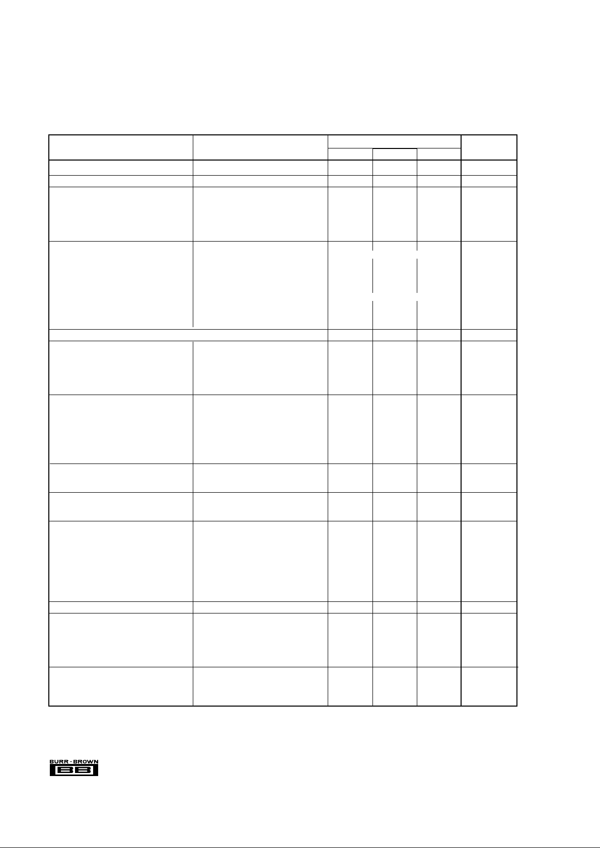
SPECIFICATIONS
ELECTRICAL
At 25°C, and ±VA = ±5.0V; +VD = +5.0V, unless otherwise noted. Where relevant, specifications apply to both left and right input/output channels.
NOTES: (1) Binary Two’s Complement coding. (2) The PCM1750 is tested and guaranteed at 5.2µs, however it will operate at 4.5µs. The dynamic performance is not
guaranteed or tested at this conversion rate. (3) Ratio of Signal
RMS
/ (Distortion
RMS
+ Noise
RMS
). (4) A/D converter sample frequency (4 x 48kHz; 4X oversampling per
channel). (5) A/D converter input frequency (signal level). (6) Referred to input signal level. (7) Ratio of (Distortion
RMS
+ Noise
RMS
) / Signal
RMS
. (8) Externally adjustable
to zero error. (9) Differential non-linearity error at bipolar major carry input code. Externally adjustable to zero error. (10) Full scale range (5.50V). (11) Refer to equivalent
circuit in Figure 1. (12) Worst case operating condition. Refer to typical performance curves.
PCM1750P, U
PARAMETER CONDITIONS MIN TYP MAX UNITS
RESOLUTION 18 Bits
DYNAMIC RANGE THD + N at –60dB Referred to Full Scale +88 +90 dB
ANALOG INPUT
Input Range ±2.75 V
Input Capacitance 20 pF
Aperture Delay 10 ns
Aperture Uncertainty (Jitter) 50 ps
rms
Full Power Input Bandwidth 500 kHz
DIGITAL INPUT/OUTPUT
Logic Family CMOS Compatible
Logic Level: V
IH
IIH = ±5µA +3.5 +VD + 0.3 V
V
IL
IIL = ±5µA –0.3 +1.5 V
V
OH
I
SOURCE
= 1.0mA +2.7 +4.7 V
V
OL
I
SINK
= 3.2mA +0.2 +0.4 V
Output Data Format Serial, MSB First, BTC
(1)
Convert Command Positive Edge
Convert Command Pulse Width 81 ns
Conversion Time Throughput Including Sample/Hold
(2)
4.5 5.2 20.8 µs
DYNAMIC CHARACTERISTICS (20Hz to 24kHz; 4X data decimated to 1X)
Signal-to-Noise Ratio
(3)
fs = 192kHz
(4)
; fIN = 1kHz (0dB)
(5)
+88 +90 dB
(6)
Total Harmonic Distortion + N
(7)
Without External Adjustments
f
IN
= 1kHz (0dB) fs = 192kHz –90 –88 dB
f
IN
= 1kHz (–20dB) fs = 192kHz –70 –68 dB
f
IN
= 1kHz (–60dB) fs = 192kHz –30 –28 dB
Channel Separation fs = 192kHz; f
IN
= 1kHz (0dB) and 0V +96 +108 dB
ACCURACY
Gain Error ±2 ±5%
Gain Mismatch Channel to Channel ±0.5 ±2.0 %
BPZ (Bipolar Zero) Error
(8)
±2mV
BPZ Error Mismatch Channel to Channel ±3mV
BPZ Differential Linearity Error
(9)
±0.002 % of FSR
(10)
Linearity Error ±0.003 % of FSR
Warm-up Time 1ms
DRIFT (With Internal Reference)
Gain 0°C to 70°C ±50 ppm/°C
Bipolar Zero 0°C to 70°C ±10 ppm of FSR/°C
DRIFT (Exclusive of Internal Reference)
Gain 0°C to 70°C ±10 ppm/°C
Bipolar Zero 0°C to 70°C ±3 ppm of FSR/°C
REFERENCE
V
REF
Output (Pins 19, 24):
Voltage +2.75 V
Current ±100 µA
Impedance 0.2 Ω
Accuracy ±25 mV
Drift 0°C to 70°C ±50 ppm/°C
V
REF
Input (Pins 18, P25):
Impedance
(11)
363 || 120 Ω || pF
POWER SUPPLY REJECTION % of V
IN
/ % of V
SUPPLY
(12)
0.03 % / %
POWER SUPPLY REQUIREMENTS
±V
A
Supply Voltage Range ±4.75 ±5.00 ±5.25 V
+V
D
Supply Voltage Range +4.75 +5.00 +5.25 V
+I
A
; +ID Combined Supply Current +VA; +VD = +5.0V +28 mA
–I
A
Supply Current –VA = –5.0V –13 mA
Power Dissipation ±V
A
= ±5.0V; +VD = +5.0V 210 300 mW
TEMPERATURE RANGE
Specification 0 +70 °C
Operating –40 +85 °C
Storage –60 +100 °C
Page 3
3
®
PCM1750
THD+N vs FREQUENCY
(Without 4X Digital Filter)
Frequency (kHz)
–20
–40
–60
–80
–100
0 20406080
100
V = –60dB
IN
V = –40dB
IN
IN
V = 0dB
IN
THD+N (dB)
V = –20dB
THD+N vs FREQUENCY
(With 4X Digital Filter)
–20
–40
–60
–80
–100
0 4 8 12 16 20 24
Frequency (kHz)
THD+N (dB)
V = –60dB
IN
V = –40dB
IN
V = –20dB
IN
V = 0dB
IN
PIN ASSIGNMENTS
PIN DESCRIPTION MNEMONIC
1 –5V Analog Supply Voltage –V
A
2 +5V Analog Supply Voltage +V
A
3 Serial Output (Left Channel) SOUTL
4 External Clock Input CLK
5 +5V Analog Supply Voltage +V
A
6 +5V Digital Voltage Supply +V
D
7 +5V Digital Voltage Supply +V
D
8 Digital Common Connection DCOM
9 Analog Common Connection ACOM
10 Digital Common Connection DCOM
11 Convert Command Input CONVERT
12 Serial Output (Right Channel) SOUTR
13 +5V Analog Supply Voltage +V
A
14 –5V Analog Supply Voltage –V
A
15 Offset Adjust (Right Channel) OFF
ADJR
16 MSB Adjust (Right Channel) MSB
ADJR
17 Analog Voltage Input (Right Channel; ±2.75V) V
INR
18 Reference Voltage Input (Right Channel) VREF
INR
19 Reference Voltage Output (Right Channel) VREF
OUTR
20 Analog Common Connection ACOM
21 Reference Voltage Decouple VREF
CAP
22 Reference Common Connection RCOM
23 Analog Common Connection ACOM
24 Reference Voltage Output (Left Channel) VREF
OUTL
25 Reference Voltage Input (Left Channel) VREF
INL
26 Analog Voltage Input (Left Channel; ±2.75V) V
INL
27 MSB Adjust (Left Channel) MSB
ADJL
28 Offset Adjust (Left Channel) OFF
ADJL
Analog Input Voltage (VIN) .................................. –VA –0.3V to +VA + 0.3V
+V
A
; +VD to ACOM/DCOM............................................................0 to +7V
–V
A
to ACOM/DCOM .................................................................... 0 to –7V
–V
A
to +VA; +VD.........................................................................0 to +14V
ACOM to DCOM .................................................................................. ±1V
Digital Inputs (pins 4, 11) to DCOM ........................... –0.3V to +V
D
+ 0.3V
Power Dissipation .......................................................................... 400mW
Lead Temperature, (soldering 10s)................................................ +300°C
Max Junction Temperature .............................................................. 165°C
Thermal Resistance,
θ
JA
: Plastic DIP............................................ 80°C/W
Thermal Resistance,
θ
JA
: Plastic SOIC .......................................100°C/W
NOTE: Stresses above those listed under Absolute Maximum Ratings may
cause permanent damage to the device. Exposure to absolute maximum
conditions for extended periods may affect device reliability.
ABSOLUTE MAXIMUM RATINGS
TYPICAL PERFORMANCE CURVES
At 25°C, and ±VA = ±5.0V; +VD = +5V, unless otherwise noted. Where relevant, specifications apply to both left and right input output channels.
PACKAGE INFORMATION
PACKAGE DRAWING
MODEL PACKAGE NUMBER
(1)
PCM1750P 28-Pin Plastic DIP 215
PCM1750U 28-Pin Plastic SOIC 217
NOTE: (1) For detailed drawing and dimension table, please see end of data
sheet, or Appendix D of Burr-Brown IC Data Book.
The information provided herein is believed to be reliable; however, BURR-BROWN assumes no responsibility for inaccuracies or omissions. BURR-BROWN assumes
no responsibility for the use of this information, and all use of such information shall be entirely at the user’s own risk. Prices and specifications are subject to change
without notice. No patent rights or licenses to any of the circuits described herein are implied or granted to any third party. BURR-BROWN does not authorize or warrant
any BURR-BROWN product for use in life support devices and/or systems.
Page 4
®
PCM1750 4
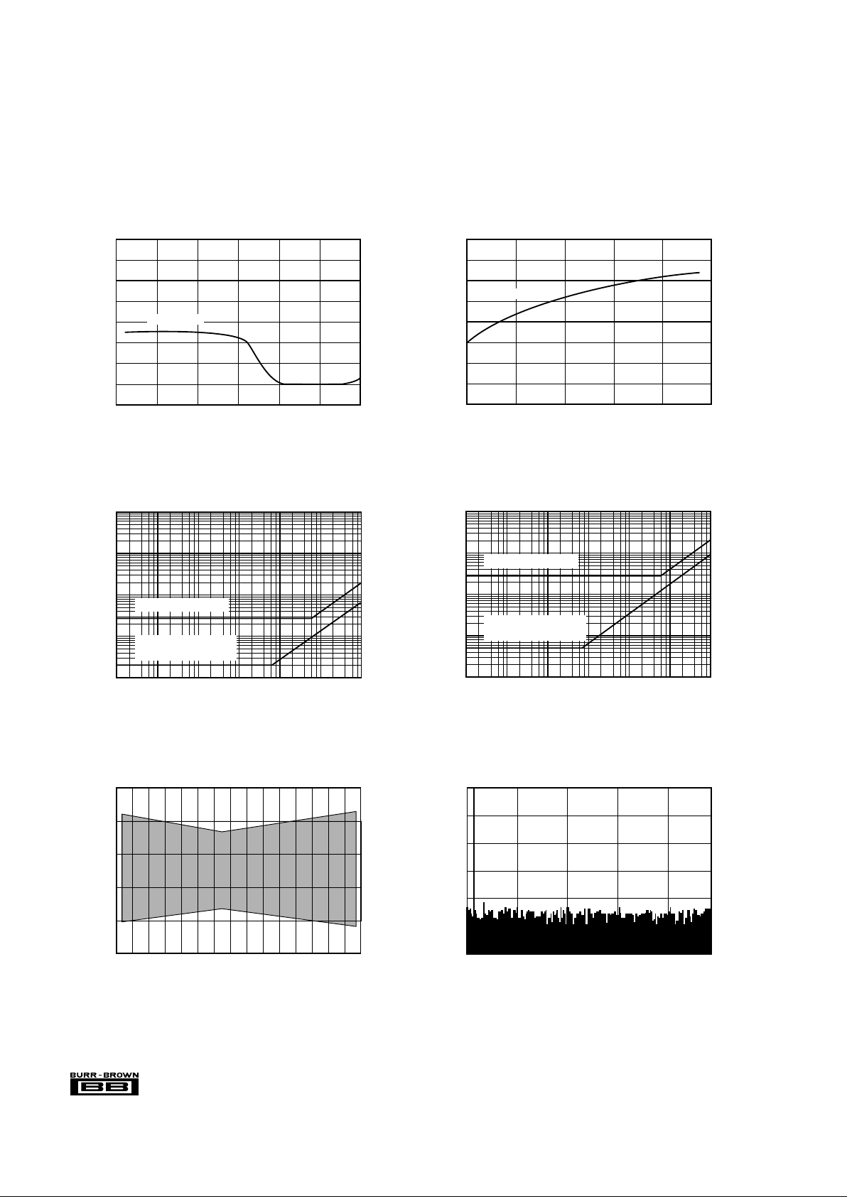
FFT 850Hz (24kHz BW; 2048 POINTS)
0
–25
–50
–75
–100
–125
–150
Amplitude (dB)
0
Frequency (kHz)
510152024
TYPICAL PERFORMANCE CURVES (CONT)
At 25°C, and ±VA = ±5.0V; +VD = +5.0V, unless otherwise noted. Where relevant, specifications apply to both left and right input-output channels.
THD vs FREQUENCY
(Without 4X Digital Filter)
Frequency (kHz)
THD (dB)
–70
–80
–90
–100
–110
0 20406080100
V = 0dB
IN
THD vs FREQUENCY
(With 4X Digital Filter)
Frequency (kHz)
–70
–80
–90
–100
–110
THD (dB)
V = 0dB
IN
0 4 8 12 16 20 24
PSR vs FREQUENCY
(–5V SUPPLY)
1
0.1
0.01
0.001
0.0001
% / %
1 10 100 1k 10k 100k 1M
Frequency (Hz)
% of V /% of V
IN SUPPLY
At BPZ:
% of FSR / % of V
SUPPLY
PSR vs FREQUENCY
(+5V SUPPLIES)
1
0.1
0.01
0.001
0.0001
% / %
1 10 100 1k 10k 100k 1M
Frequency (Hz)
% of V /% of V
IN SUPPLY
At BPZ:
% of FSR / % of V
SUPPLY
V vs TEMPERATURE
(V Outputs)
Temperature in °C
2.80
2.78
2.76
2.74
2.72
2.70
–40 –20 0 20 40 60 80 100
V
REF
(V)
REF
REF
Page 5
5
®
PCM1750
FFT 88kHz and 92kHz (96kHz BW; 16384 POINTS)
0
–25
–50
–75
–100
–125
–150
Amplitude (dB)
0
Frequency (kHz)
20 40 60 80 96
–6dB
FFT 92kHz (96kHz BW; 2048 POINTS)
0
–25
–50
–75
–100
–125
–150
Amplitude (dB)
0
Frequency (kHz)
20 40 60 80 96
FFT 20kHz (24kHz BW; 2048 POINTS)
0
–25
–50
–75
–100
–125
–150
Amplitude (dB)
0
Frequency (kHz)
510152024
TYPICAL PERFORMANCE CURVES (CONT)
At 25°C, and ±VA; +VD = ±5V, unless otherwise noted. Where relevant, specifications apply to both left and right input-output channels.
FFT 17kHz and 21kHz (24kHz BW; 16384 POINTS)
0
–25
–50
–75
–100
–125
–150
Amplitude (dB)
0
Frequency (kHz)
510152024
–6dB
FFT 3.7kHz (96kHz BW; 2048 POINTS)
0
–25
–50
–75
–100
–125
–150
Amplitude (dB)
0
Frequency (kHz)
20 40 60 80 96
FFT 52kHz (96kHz BW; 2048 POINTS)
0
–25
–50
–75
–100
–125
–150
Amplitude (dB)
0
Frequency (kHz)
20 40 60 80 96
Page 6
®
PCM1750 6
25k
25k
150k
5k
5k
12a
3b
3a
2b
1b
1a
2T
1T
3T
12T
off
S
C
V
REF
P16, P27
+V (+5V)
P15, P28
.01µF
P19, P24
500
13.25k
A1
A2
Latch
Comparator
Data Out
AZ
CAZ
(MSB)
S
V
C
10PF
1
2
3
IN
REF
5PF
20PF
1
L
V
S
S
3
C
2
C
1
1
CAZ
2
AZ
2
AZ
CAZ
3
3
CAZ
4
AZ
4
47k
A
.01µF
+V (+5V)
A
off
C
R
offb
500
R
12b
R
S
12T
R
R
R
S
3T
C
S
2T
C
S
1T
C
R
R
a
b
R
R
Ω
Ω
Ω
Ω
Ω
Ω
Ω
2a
R
Ω
Ω
100mV
H1 H2
P18, P25
V
Simplified
V Circuit
REFIN
REFIN
+V (+5V)
A
917
Ω
P18, P25
V
REFIN
R
offa
47k
Ω
V
REFOUT
Optional External
Adjustment Circuitry
TDAC
Auto-Zeroed Comparator
CDAC
0 to 120pF
(Code
dependent)
MSB Adj
Off Adj
= 2.75V
600
Ω
13.25k
Ω
THEORY OF OPERATION
OVERVIEW
The PCM1750 is a dual 18-bit successive approximation
CMOS analog-to-digital converter with serial data outputs
designed especially for digital audio and similar applications. The single-chip converter is fabricated on a 3µ P-well
CMOS process which includes poly-poly capacitors, lasertrimmable nichrome resistors, and two layers of interconnect
metal. The dual converter employs a switched capacitor
architecture which provides separate, simultaneous S/H
(sample/hold) functions for each input channel. The separate
S/H for each channel results in a desired feature called
co-phase sampling which means that both S/H circuits are
switched at the same time into the HOLD mode to capture
their respective input signals simultaneously. This eliminates phasing errors produced by alternative architecture
ADCs which do not sample the two input channels at the
same time.
Switched binary-weighted poly-poly capacitors are used in
CDAC (capacitive digital-to-analog converter) configurations to form the successive approximation converter sec-
FIGURE 1. PCM1750 Simplified Circuit Diagram.
Page 7

7
®
PCM1750
tions of the PCM1750. Two other switched-capacitor TDACs
(trim-DACs, which employ laser-trimmed nichrome resistors) are also used to provide small correction voltages to the
latching comparators. These small correction voltages compensate for ratio matching errors of the binary-weighted
capacitors in the CDAC. The comparators contain autozeroed
preamplifier stages ahead of the latching amplifier stage to
produce a one bit, serial data stream that controls the
successive approximation algorithm for each channel of the
PCM1750.
To simplify user application, the PCM1750 includes an
internal band-gap reference with fast settling buffer amplifiers to drive the CDACs. The dual converters operate synchronously (to minimize digital noise conversion errors)
using an external system clock (normally at 1X, 2X or 4X
the standard 48kHz audio sampling rate). By operating at a
2X or 4X oversampling rate the roll-off requirement for the
input anti-aliasing filters is relaxed. For example, 1X systems typically use a 9 to 11 pole LPF (low pass filter)
whereas a 4X system can use a 6th (or smaller) order filter
when an appropriate digital filter such as the DF1750 is used
in conjunction with the sampling system. Oversampling also
has the added benefit of improved signal to noise ratio and
total harmonic distortion. Two serial outputs, one for each
input channel, provide binary-two’s-complement coded output to an optional external digital decimation filter when
over sampling operation is desired. The use of the optional
companion digital filter, the DF1750, is described later in
the installation and application sections of this product data
sheet. A separate product data sheet is also available for the
Burr-Brown DF1750 giving all the specifications and performance diagrams associated with this digital filter.
SAMPLE (TRACKING) MODE
After each conversion, the dual ADC returns to the SAMPLE
mode in order to track the input signals. The switches shown
in the simplified circuit diagram of Figure 1 will then be in
the following states: S1 connects V
IN
to C1 ; S2 to S18
connect C2 to C18 to V
REF
; H1 and H2 connect the top
plates of the capacitor arrays to analog common; and the
latching comparator is switched into its auto-zero mode by
closing AZ1 to AZ4. Notice that C1 serves two purposes: it
samples and stores the input signal V
IN
and it is the MSB of
the CDAC. Storing V
REF
on C2 to C18 creates a bipolar
offset, enabling V
IN
to cover a span from –V
REF
to +V
REF
.
The 1/f noise as well as the DC input offset voltage of the
comparator are removed by an autozeroing cycle which
* Clock from optional digital filter chip (DF1750 4x decimation filter).
P11 (CONVERT)
P4 (EXT CLK IN)
3
4
1
2
18 1916 17
*Master
System
Clock
64 1 2 3 4 5 6 7 8 9 10111213141516 50 515253 54 55 56 57 58 59 60 61 62 63 64 1 2
Bit 1
MSB
Bit 2
Bit 3
Bit 16 Bit 17
Bit 1
MSB
Bit 2
Bit 3 Bit 16 Bit 17
Bit 4
Bit 4
Bit 18
LSB
Bit 18
LSB
INTERNAL
S/H
CONTROL
SR1
SR2
SR3
P3 (SOUT L)
P12 (SOUT R)
Bit 3 test time
Bit 2 test time
Bit 1 test time
HOLD SAMPLE
FIGURE 2. PCM1750 Input/Output Timing Diagram.
Page 8

®
PCM1750 8
occurs during the SAMPLE period (see the timing diagram
shown in Figure 2). These errors are stored on the AC
coupling capacitors (CAZ1 to CAZ4, shown in Figure 1)
between the gain stages. During the SAMPLE period the
inputs to gain stages A1 and A2 and the latch are grounded
by switches H1, H2, and AZ1 to AZ4. Capacitors CAZ1 and
CAZ2 track the amplified offset voltage of gain stage A1
and capacitors CAZ3 and CAZ4 do the same for A2. At the
beginning of a conversion cycle, the autozeroing switches
open and the instantaneous amplified value of both the DC
offset voltage and the low-frequency flicker noise is stored
on the coupling capacitors to produce zero comparator offset
during a conversion cycle.
SUCCESSIVE APPROXIMATION
CONVERSION PROCESS
The timing diagram in Figure 2 illustrates the successive
approximation routine of the PCM1750. Control signals
CONVERT and CLK are derived from a master system
clock which comes from a 256f
S
(256 X the base sampling
frequency of 48kHz) clock used by the optional digital filter.
There are 64 clocks shown in the timing diagram because the
PCM1750 is shown operating at 4 times the standard 48kHz
sample rate (192kHz).
Several events occur on the rising edge of the CONVERT
command. Switches AZ1 to AZ4, H1 and H2 open and
switch S1 reconnects the MSB capacitor, C1, from V
IN
to
analog common (see Figure 1). This terminates the comparator auto-zero cycle and simultaneously switches (cophase sampling) both converters from tracking their respective input signals into the HOLD mode, thus capturing the
instantaneous value of V
IN
(with a small delay specified as
the aperture time).
At the start of a conversion cycle when S1 is switched to
analog common, the sampled input signal V
IN
will appear at
the comparator input as –V
IN
/2 due to the 2-to-1 capacitive
divider action of Cl = C2 + C3 + ... C18. In a somewhat
similar manner, V
REF
is transferred to the comparator input
as –V
REF
/2 to create a bipolar offset.
The 19-bit shift register, shown in Figure 4, controls testing
of the bits of the dual ADCs beginning with bit-1 (MSB) and
proceeding one bit at a time to bit-18 (LSB), leaving ON
those bits that don’t cause the cumulative value of the
CDAC to exceed the original input value and leaving OFF
those bits that do. Since the bits of both channels are tested
together, only one shift register is required to control both
ranks of 18 data latches.
For example, the testing of bit-2 proceeds in the following
manner. The positive pulse from the second shift register
element SR2, (see Figure 2 and 4) is applied to the bit-2 data
latch and NOR gate. The NOR gate in turn drives S2 and
switches bit-2 at the beginning of the bit-2 test interval. Note
that the bit interval must be long enough to allow both the
comparator input to settle and the comparator to respond. On
1
2
18 19 3
*Optional
Digital Filter
54
555657 58 59 606162 63 64123456
78910 11 12
T1
T4
T6
T3
T5
T7
T9
REF
T
Convert
Ext Clk In
SOUT
Bit 18
LSB
Bit 1
MSB
Bit 2
Bit 17
T8
T2
PARAMETER DESCRIPTION MIN NOMINAL MAX UNITS
T1 (1 x TREF) Convert Command High 24 33 55 % of T4
T2 (6 x TREF) S/H Acquisition Time 420 486 ns
T3 (4 x TREF) Convert to Clock time 281 326 1302 ns
T4 (3 x TREF) Master Clock Input 211 244 977 ns
T5 (1 x TREF) Clock High 24 33 55 % of T4
T6 (2 x TREF) Clock Low 45 67 76 % of T4
T7 Data Hold Time 10 ns
T8 Data Setup Time 100 ns
T9 Data Valid Time 120 154 1212 ns
TCONV (64 x TREF) Conversion Throughput Time 4.5 5.2 20.8 µs
TREF (Sample Rate /64) Ext Digital Filter Clock 70 81 326 ns
Note: The nominal timing shown in this diagram is all done automatically by the DF1750 digital filter. Only the
optional digital filter clock is required when the DF1750 is used.
FIGURE 3. PCM1750 Setup and Hold Timing Diagram.
Page 9

9
®
PCM1750
the next rising edge of CLKIN, at the end of the test interval,
the comparator latch is strobed, providing a feedback logic
level which tells the second data latch if bit-2 should be kept
or rejected. This logic level is stored in the data latch and is
passed on to switch S2 via the NOR gate on the falling edge
of the pulse from SR2. This decision to keep or reject bit-2
moves the comparator input closer to a null condition,
namely, zero potential. This sequential process continues for
bit-3 through bit-18 and nulls the comparator inputs to
within a value limited by the total system noise and the
resolution/speed of the comparator.
Notice from the timing diagram in Figure 2 that the successive approximation algorithm operates synchronously with
an external clock to minimize digitally-coupled switching
noise from corrupting either the sample-to-hold operation or
the critical comparator bit decisions. The two serial output
data streams are derived synchronously from the respective
latched comparator outputs and are available after a delay of
one CLKIN cycle as illustrated in Figure 2. The serial output
driver cells are TTL and CMOS compatible.
DIFFERENTIAL LINEARITY CALIBRATION
To understand the calibration of the PCM1750 it is necessary to discuss some of the characteristics of poly-poly
capacitors. Poly capacitors are known to have equal or better
stability and matching properties when compared to other
precision components such as thin film resistors. On a well
controlled process, ratio matching is typically 0.1%— a
very respectable number for an untrimmed component. Even
more impressive is their ratio tracking versus temperature of
approximately 0.1ppm/°C.
Achieving DLE (differential linearity error) of less than 1/2
LSB at the 16-bit level requires ratio matching of the more
significant bits to about 0.001%. Since the untrimmed ratio
matching of poly capacitors is about two orders of magnitude larger than this requirement, a one-time factory calibration of the upper bits is required as described in the next
section. Next, consider the effect of temperature due to the
ratio tracking of 0.lppm/°C. Over a 50°C span, DLE will
change less than 1LSB at 18-bits; therefore, recalibration at
temperature extremes is not necessary. Because of this
excellent stability versus temperature (and versus time, also),
the one-time factory calibration to correct initial DLE is
more than satisfactory in meeting the accuracy requirements
of the PCM1750.
TDAC OPERATION
Operation of the TDAC (trim DAC), which is laser trimmed
at the wafer level, is described using bit-1 as an example.
Switch S1T (see Figure 1) operates between two voltage
levels—a reference level set by voltage divider Ra, Rb and
a laser trimmable level set by R1a, R1b. The differences of
these two levels is coupled by capacitor C1T to the minus
input of the comparator to generate a correction voltage for
DQ
LR
DQ
R
SR
2
DQ
L
R
DQ
L
R
DQ
R
SR
18
DQ
L
R
DQ
L
R
DQ
S
SR
1
DQ
L
R
DQ
R
SR
19
Control
Logic
To MSB
Switches Left
To Bit 2
Switches Left
To Bit 18
Switches Left
To MSB
Switches Right
To Bit 2
Switches Right
To Bit 18
Switches Right
Serial Data
From Latching
Comparator
Serial Data
From Latching
Comparator
Data
Latches
Left Channel
19-Bit
Shift
Register
Data
Latches
Right Channel
FIGURE 4. PCM1750 Successive Approximation Logic Diagram.
Page 10

®
PCM1750 10
A Gain Change
Rotates
Transfer
Function
Offset Change
Shifts
Transfer
Function
1FFFF
H
1FFFE
H
00001
00000
H
3FFFF
H
20001
H
20000
H
Digital Output
* Gain drift (mostly due to reference drift) rotates the transfer function
around the bipolar zero code (00000 ).
NOTE: As the power supply voltages change (mostly due to the +V
supply), the transfer function rotates around BPZ. See the power
supply rejection specification in the spec table.
0.00V
+2.749979–20.98µV–2.75
HEX
H
bit-1. The switches of the CDAC and the switches of the
TDAC operate concurrently with each other, that is, when a
decision is made to keep or reject bit-1, the same decision is
made for the correction voltage for bit-1. Even though the
ratio stability of the nichrome resistors used in the TDAC
may not be as good as the poly capacitors, it is inconsequential because the correction voltage of each bit has a limited
range of adjustment.
The DLE at the major carry (a code change from 111...111
to 000...000; in binary two’s complement coding) is typically ±1/2 LSB at the 16-bit level, which is sufficient to
provide 90dB SNR and –30dB low level distortion (–60dB
input). For applications requiring less DLE at the major
carry, a pin is provided for each channel to make an external
MSB adjustment.
DISCUSSION
OF SPECIFICATIONS
RESOLUTION AND DYNAMIC RANGE
The theoretical resolution of the PCM1750 is 18-bits. The
maximum possible number of output codes or counts at 18bits is 262,144 or 108dB (calculated by raising 2 to the 18th
power). The relative accuracy of any A/D converter, however, is more a function of it’s absolute linearity and signalto-noise ratio than how many bits of resolution it has. These
more pertinent specifications are described later in this
section.
Dynamic range, as it is usually defined for digital audio
converters, is the measure of THD+N at an effective input
signal level of –60dB referred to 0dB. For the PCM1750 this
value is typically 90dB and a minimum of 88dB (for audio
bandwidth = 20Hz to 24kHz, THD+N at –60db = –30 db typ,
–28dB max; f
IN
= 1kHz and fS = 192kHz). Resolution is also
commonly used as a theoretical measure of dynamic range,
but it does not take into account the effects of distortion and
noise at low signal levels.
ANALOG INPUT RANGE
The analog input range for the PCM1750 is a bipolar ±2.75V
(nominal). Table I gives the precise input/output and voltage/code relationships for the PCM1750. Figure 5 shows
these same relationships in a graphical format. It should be
noted that the computed voltage input levels represent center
values (the midpoint between code transitions). Output coding is in binary two’s complement.
DIGITAL OUTPUT ANALOG INPUT VOLTAGE INPUT
262144 LSBs Full Scale Range 5.50000000V
1 LSB Minimum Step Size 20.98083496µV
1FFFF
HEX
+Full Scale +2.74997902V
00000
HEX
Bipolar Zero 0.00000000V
3FFFF
HEX
Bipolar Zero –1LSB –0.00002098V
20000
HEX
–Full Scale –2.75000000V
TABLE I. Analog Input to Digital Output Relationships.
From Figure 5, the effects of offset and gain errors can be
visualized. These errors can change value in response to
changes in temperature and/or supply voltage. In addition,
gain error (or the full scale range, FSR) changes in direct
proportion to the VREF
IN
voltage value.
SAMPLE AND HOLD PARAMETERS
Aperture Delay and Uncertainty
Aperture delay is the time required to switch from the
SAMPLE to HOLD mode. This time is typically 10ns for the
PCM1750 and it is constant. Aperture uncertainty (jitter) is
the amount of uncertainty associated with the aperture delay.
Aperture uncertainty affects the overall accuracy of the
converter and is greatest at the maximum input frequency of
the converter. The formula for determining the maximum
input frequency (f
MAX
) for a given error contribution due to
aperture uncertainty is: f
MAX
=(2XπXt
jitter
X 2N)–1 where
t
jitter
is the RMS aperture uncertainty and 2N is the desired
SNR (signal-to-noise ratio) expressed in total number of
quantization levels. A 15-bit SNR, therefore, would be
expressed as 2
15
or 32768. Using the typical PCM1750
aperture jitter of 50ps
rms
and an SNR at the 15-bit level, f
MAX
= (2 X π X 50ps X 32768)–1 or 97.1kHz. This matches very
closely with the rated dynamic accuracy of the PCM1750
where THD+N = –88dB max. This means the typical aperture jitter of PCM1750 only becomes a factor when input
signals to it exceed 97kHz and/or an SNR greater than 15
bits is desired.
Input Bandwidth
The full power bandwidth of the PCM1750 is that input
frequency above which significant distortion is observed
(THD+N > 10-bits or –60dB for a full scale input signal). In
the data sheet, this number is specified as typically being
500kHz. In wideband operation (when no digital filter is
used) the additional full power bandwidth of the PCM1750
FIGURE 5. Analog Input to Digital Output Diagram.
Page 11

11
®
PCM1750
can be used to purposely alias a band-limited signal down
into the baseband of the converter. This technique is called
undersampling and can be used to directly down-convert an
intermediate frequency riding on a much higher carrier
frequency.
DIGITAL I/O AND TIMING
Input/Output Logic Compatibility
Digital logic on the PCM1750 is CMOS compatible. Digital
outputs on the PCM1750 are capable of driving a minimum
of two standard TTL input loads.
Digital output coding is in binary two’s complement. Table I
gives the precise input/output voltage/code relationships for
the PCM1750. Figure 5 shows these same relationships in a
graphical format.
Convert Command and External Clock Input
A conversion is initiated on its positive going edge of the
convert command. Although the convert command can return low at any time (prior to 50ns before the rising edge of
the 19th clock), a typical convert command pulse width of
81ns (as called out in Figure 3) is specified for a 192kHz
sample rate (f
S
). The reason for a pulse width spec is to
reduce problems associated with digital logic feedthrough
noise. The return of convert command to a logic low level in
the specified time interferes least with the successive approximation process. Also, it should be noted that putting
fast logic edges (<5ns) on convert command (P11) and the
external clock input (P4) may cause logic feedthrough to the
analog stages in the converter and will result in added
distortion during the sampling and conversion process.
Using the optional DF1750 digital filter provides adequately
slow transitions to maintain full specification performance.
If necessary, an external RC, on the convert command line
may be used to slow fast logic edges.
As with the convert command, the external clock input is
positive edge triggered and is not duty-cycle dependent
other than to improve digital feedthrough noise immunity. A
50% duty cycle clock can be used instead of 33% if desired.
Refer to Figure 3 for recommended timing relationships.
Regardless of what clock duty cycle is used, all operations
relating to valid data clocking should be synchronized to the
rising edge of the clock input.
Although there is a maximum conversion time called out in
the specification table, the PCM1750 can have a considerably longer conversion cycle. Droop of the internal capacitors will ultimately determine what the true maximum
conversion time can be. The min/typ/max times shown in
Figure 3 are based on minimum sample rate of 48kHz, a
typical of 192kHz, and a maximum of 222kHz. All specifications are tested at 192kHz. The minimum sample rate
assumption is based on clock periods that increase as time
between convert commands increases. Any sample rate
down to near DC can be utilized by observing maximum
clock cycle requirements and spacing convert commands to
achieve lower sample rates. This means that the time interval
T2 shown in Figure 3 does not have a maximum value.
Clock Lockout
Any number of clocks can be given to the PCM1750 beyond
the 19 required for normal operation. If a continuous clock
is used, all clocks beyond the 19th are gated off by the
PCM1750’s internal logic until the next positive going edge
of the convert command. The converter also goes into the
sample (track) mode starting on the positive edge of the 19th
clock until the next positive edge of the convert command,
regardless of how many additional clocks are offered. The
ideal operation of the converter stops the clock input after
the 19th during this critical signal acquisition time. This is
the timing shown in Figure 3 . The critical timing aspect that
must be observed if a clock input other than the recommended is used, is that ample time following the positive
edge of convert command proceed the next rising clock
edge. If this time is shortened, the most important bit-1
(MSB) decision, which is finalized on the first clock edge
after convert command, will be adversely affected. In other
words, the clock input cannot have a rising edge during the
time interval T3 shown in Figure 3.
SIGNAL-TO-NOISE RATIO
Another specification for A/D converters is signal-to-noise
ratio (SNR). For this measurement, a full-scale 1kHz signal
is applied and the sampling rate of the PCM1750 is set at
192kHz. An FFT is performed on the digital output and the
noise power in the non-harmonic audio-bandwidth frequency
bins (20Hz to 24kHz) is summed and expressed in relation
to the full-scale input signal.
One advantage of using the PCM1750 in this oversampled
mode with the optional DF1750 digital decimation filter is
that the converter noise is spread over the full 0Hz to 96kHz
passband and then suppressed by the digital filter stopband
attenuation (from 24kHz to 96kHz). This effectively increases the SNR of the PCM1750 by 6dB when it is used as
an audio bandwidth converter. The other advantage is that
the need for a higher-order anti-aliasing input filtering is
greatly reduced.
THD + N
The key specification for the PCM1750 is total harmonic
distortion plus noise (THD+N). In terms of signal measurement, THD+N is the ratio of Distortion
RMS
+ Noise
RMS
/
Signal
RMS
expressed in dB. For the PCM1750, THD+N is
100% tested at all three specified input levels using the
production test setup shown in Figure 6. For this measurement, as with the SNR test, a full-scale 1kHz signal is
applied and the sampling rate of the PCM1750 is set at
192kHz (which is 4X the standard digital audio sample rate
of 48kHz). An FFT is performed on the digital output and
the total power in all audio-bandwidth frequency bins (20Hz
to 24kHz) is summed and expressed in relation to the fullscale input signal.
For the audio band, the THD+N of the PCM1750 is essentially flat for all frequencies and input signal levels. In the
Typical Performance Curves THD+N versus Frequency
Page 12

®
PCM1750 12
plots are shown at four different input signal levels (with and
without a 4X decimation filter): 0dB, –20dB, –40dB, and –
60dB.
CHANNEL SEPARATION
To test channel separation a 1kHz signal sampled at 192kHz
is placed on one input of the PCM1750 while the other input
is held at 0V. An FFT is performed on the idle (0V) channel
and the result checked to insure that the 1kHz tone is
suppressed by a minimum of 96dB.
GAIN AND OFFSET ERRORS
Initial gain and bipolar offset errors are laser trimmed at the
wafer level and 100% final tested to insure compliance with
the electrical specifications. Bipolar offset errors can be
further reduced to zero by using the optional offset adjustment circuitry shown in the connection diagram (Figure 7).
Gain errors can be adjusted by varying V
REF
to either
channel of the converter. This is accomplished by either
using an adjustable external reference or by placing buffer
amplifiers with adjustable gain between VREF
OUT
and
VREF
IN
as shown in Figure 8a.
INTEGRAL AND DIFFERENTIAL LINEARITY
DC Linearity Testing
The absolute linearity of the PCM1750 is on the order of 15
bits or more as can be seen from the THD versus Frequency
plots in the Typical Performance Curves. Not every code in
the converter must be 15-bit linear to achieve the specified
THD+N performance, but a very high percentage will be
that linear. The same observation also applies to differential
linearity errors in the PCM1750. Because the PCM1750 is
not 100% tested for DC linearity specifications, no minimum or maximum specifications are given for integral or
differential linearity errors.
No Missing Codes Operation
A no missing codes specification is not given for the
PCM1750 for the same reasons as given above. The
PCM1750, however, typically has fewer than 16 codes (less
than 0.01%) missing at a 14-bit resolution level. A 100% no
missing codes specification cannot be maintained above the
12-bit level, although this has very little impact on overall
dynamic performance (THD+N). The few missing codes
that do occur at higher resolution levels are at the bit-2 and
lower major carry transitions of the converter. There are
typically no missing codes (at 14 bits) around the critical
bipolar zero operation zone (±1/8 of full scale range around
bipolar zero or 0V). The critical bipolar differential linearity
error can be reduced from its initial value to zero using the
optional MSB adjustment circuitry shown in the connection
diagram (Figure 7).
REFERENCE
The gain drift of the PCM1750 is primarily due to the drift
associated with the reference. Better drift performance can
be achieved using an external reference like the ones explained in the applications section (Figures 8b, 8c). The
Typical Performance Curves plot of V
REF
Output versus
Temperature shows the full range of operation including
initial error and typical gain drift. Pertinent performance
data are found in the electrical specification table.
Reference Bypass
Both P18 and P25 (VREF
IN
) should be bypassed with a
10µF to 47µF tantalum capacitor. If there are important
system reasons for using the PCM1750 reference externally,
the outputs of P19 and P24 must be appropriately buffered,
and bypassed (see Figure 8).
FIGURE 6. PCM1750 Production Test Setup.
PCM1750
Low Pass
Filter
FTT
Analyzer
High
Accuracy
Sine Wave
Generator
Timing
Control
f = 192kHz
f = 1kHz
Serial Data Left
Serial Data Right
IN
V
INL
INR
V
s
Parametric
Tester
Page 13

13
®
PCM1750
POWER SUPPLY REJECTION
Because of the architecture of the PCM1750, power supply
rejection varies with input signal size. The spec table value
is expressed in the relative terms of percent of V
IN
per
percent change of the supply voltage. The PSR versus
Frequency plot in the Typical Performance Curves show
PSR expressed versus an increase in power supply ripple
frequency.
PERFORMANCE OVER TEMPERATURE
Specification Temperatures
All critical specifications are tested at 25°C. The drift
specification temperature range is from 0°C to +70°C. The
PCM1750 will operate over the wider temperature range of
–40°C to +85°C.
Gain and Offset Drift
Although the PCM1750 is primarily meant for use in dynamic applications, specifications are also given for more
traditional DC drift parameters such as temperature gain and
offset drift. The primary cause of drift in the PCM1750 is the
bandgap reference. Much lower gain drift can be realized if
necessary by using any circuit similar to the external reference circuits shown in Figure 8. Also, refer to the Typical
Performance Curves of V
REF
Output versus Temperature.
Dynamic Performance
Dynamic performance is predominated by the absolute linearity of the PCM1750. Because of the excellent ratio
tracking versus temperature of poly-poly capacitors, there is
virtually no change in dynamic performance of the converter
over temperature (primarily THD+N). The dynamic specifications over temperature cannot be guaranteed, however, as
they are not 100% tested.
INST ALLATION
ANTI-ALIASING FILTER
To prevent unwanted input signals from being aliased into
the passband of the converter, it is necessary to suppress all
out of band signals above 1/2 the sampling frequency of the
ADC by using a low-pass filter. The requirement for an antialiasing filter, however, can be reduced by using oversampling
techniques. By raising the sample rate of the converter by a
factor of 2 or even 4, the roll off of the anti-aliasing filter can
be reduced. In Figure 9, a 6th order, linear-phase, antialiasing filter is implemented using low-cost dual audio op
amps. This filter will suppress frequencies above 96kHz by
80dB. For many applications a 4th or 2nd order anti-aliasing
filter will be adequate when using the PCM1750 in the 4x
oversampling mode.
FIGURE 7. PCM1750 Connection Diagram.
+
10µF*
or
47µF
0.1µF
150kΩ
25kΩ
47kΩ
25kΩ
+
10µF*
or
47µF
10µF*
+
+5V
–5V
= Connect directly to ground plane
Optional External Adjust
–V
+V
SOUT Left
Ext Clk In
+V
+V
+V
DCOM
ACOM
DCOM
Convert
SOUT Right
+V
–V
Offset Adj Left
MSB Adj Left
V Left
Ref In Left
Ref Out Left
ACOM
Ref Com
Ref Bypass
ACOM
Ref Out Right
Ref In Right
V Right
MSB Adj Right
Offset Adj Right
IN
IN
A
A
D
D
D
A
A
1
2
3
4
5
6
7
8
9
10
11
12
13
14
150kΩ
25kΩ
47kΩ
25kΩ
Optional External Adjust
10Ω
10Ω
10µF*
+
220pF
150Ω
220pF
47kΩ
0.01µF
0.01µF
0.01µF
0.01µF
47kΩ
(low
leakage,
ceramic)
* High quality tantalum.
28
27
26
25
24
23
22
21
20
19
18
17
16
15
150Ω
Page 14

®
PCM1750 14
INPUT SIGNAL CONDITIONING
RC Input Circuit
Note the 150Ω resistors and 220pF capacitors on each
analog input as shown in the connection diagram (Figure 7).
This input circuit configuration is required to achieve optimum SNR performance of the PCM1750. Various other
component values will yield satisfactory results, but the
resistor should never exceed 200Ω.
Buffer Amplifier
To avoid introducing distortion, the PCM1750 input must be
driven by a low active impedance source (op amps such as
the NE5532, Burr-Brown OPA2604, or equivalent are ideal).
EXTERNAL ADJUSTMENTS
The simplified circuit diagram (see Figure 1) shows one of
two complete channels on the PCM1750. The input switched
capacitors, trim DAC and comparator are detailed. The trim
DAC switches are activated whenever the corresponding bit
is chosen during the successive approximation routine. The
first 12 bits of the ADC have corresponding trim DAC
circuits. The R1a to R12a and R1b to R12b resistors can be
laser trimmed at the wafer level if necessary to correct for
any nonlinearities. The nominal voltage for the internally
generated V
REF
is 2.75V and it is a relatively low impedance, buffered voltage output. It should be noted that just
the act of connecting the optional adjustment circuits will
affect the MSB DLEs and bipolar offsets since it is unlikely
that the initial potentiometer settings (even if centered)
would match the factory trimmed null potentials. If connected, the potentiometers must be properly adjusted.
MSB Adjust
The MSB adjust pin connects to the center of the R1a/R1b
resistive divider for bit-1. After laser trimming this point is
nominally 100mV. All the MSB and offset adjust pins
should be connected to ground using a 0.01µF capacitor,
especially if traces to the potentiometers are long. If the
adjust pins are not used, they should still be bypassed to
ground.
Since there are internal 5kΩ resistors and clamp diodes to
both ground and +5V on the MSB and offset adjust pins,
there are obvious limits to their range of adjustment. With a
nominal internal voltage on these points of +100mV, there
will be a greater limitation in making negative adjustments
than positive. A negative voltage at either adjustment pin,
however, is acceptable up to one diode drop (–0.6V) below
ground.
The preferred method of MSB DLE adjustment is to input a
small level signal and adjust for minimum THD+N.
Offset Adjust
The offset adjust switch (S
OFF
) position is controlled by
whether the ADC is in the sample or hold mode. Switching
from sample to hold effectively allows any charge offsets
associated with the sampling process to be eliminated.
Grounding the input to the converter as far ahead of the A/D
as possible (in front of the anti-aliasing filter for example)
and then adjusting the bipolar zero error will remove the
offsets associated with the entire sampling system.
LAYOUT CONSIDERATIONS
Power Requirements
Noise on the power supply lines can degrade converter
performance, especially noise and spikes from a switching
power supply. Appropriate supplies or filters must be used.
Although the PCM1750 positive supplies have separate
digital and analog +5V, for most applications the +5V
digital supply pins should be connected to the +5V analog
supply. If they aren’t connected together, a potential latchup
condition can occur when the power supplies are not turned
on at the same time. If one supply pin is powered and the
other is not, the PCM1750 may latch up and draw excessive
current. In normal operation, this is not a problem because
both +V
A
and +VD should be connected together. However,
during evaluation, incoming inspection, repair, etc., where
the potential of a “hot” socket exists, care should be taken to
power the PCM1750 only after it has been socketed.
All supplies should be bypassed as shown in Figure 7. The
bypass capacitors should placed as close to their respective
supply pins as possible. Additional .01µF capacitors may be
placed in parallel with the larger value capacitors to increase
high-frequency rejection, but generally they are not required
when high quality tantalums are used. The 0.1µF capacitor
between P21 and P22 should be a low leakage type (such as
ceramic) and must be put as close to these pins as possible
to reduce noise pickup.
FIGURE 8a. Circuit for External Gain Adjustment Using the
Internal Reference.
10µF
+
18
1kΩ
19
1/2 5532
VREF
VREF
INR
OUTR
10µF
+
25
1kΩ
24
1/2 5532
VREF
VREF
INL
OUTL
39kΩ
+5V
–5V
+5V
–5V
50kΩ 50kΩ
1µF
+
1µF
+
39kΩ
Page 15

15
®
PCM1750
The PCM1750 is sensitive to supply voltages outside the
absolute maximum ratings shown in the specification tables.
Do not exceed –8V on the negative supplies at any time or
irreversible damage may occur. Note the 10Ω resistors in
series with each –5V supply line (shown in Figure–7) to help
protect the part from severe damage if the supplies are overranged momentarily.
Grounding Requirements
Because of the high resolution and linearity of the PCM1750,
system design problems such as ground path resistance and
contact resistance become very important.
The ACOM and DCOM pins are separated internally on the
PCM1750. To eliminate unwanted ground loops, all commons (both analog and digital) should be connected to the
same low-impedance ground plane. This should be an analog ground plane separate from other high-frequency digital
ground planes on the same board. If the analog and digital
commons of the PCM1750 are connected to different ground
planes, care should be taken to keep them within 0.6V of
each other to insure proper operation of the converter.
A ground plane is usually the best solution for preserving
dynamic performance and reducing noise coupling into
sensitive converter circuits. Where any compromises must
be made, the common return of the analog input signals
should be referenced to the ACOM pins. This will prevent
voltage drops in the power supply returns from appearing in
series with the input signal.
Coupling between analog input and digital lines should be
minimized by careful layout. For instance, if the lines must
cross, they should do so at right angles. Parallel analog and
digital lines should be separated from each other by a pattern
connected to common.
If external MSB and offset adjust potentiometers are used,
the potentiometers and related resistors should be located as
close to the PCM1750 as possible.
Minimizing “Glitches”
Coupling of external transients into an analog-to-digital
converter can cause errors which are difficult to debug. Care
should be taken to avoid glitches during critical times in the
sampling and conversion process. Since the PCM1750 has
an internal sample/hold function, the signal that switches it
into the HOLD state (CONVERT going HIGH) is critical, as
it would be on any sample/hold amplifier. The CONVERT
rising edge should have minimal ringing, especially during
the 20ns after it rises.
APPLICATIONS
USING A DIGITAL FILTER
A 4x decimation filter is available for the PCM1750 called
the DF1750. It is available in a 28-pin DIP or a 40-pin SOIC
package. The use of this filter greatly eases the implementation of the PCM1750 in audio band applications.
10µF
+
18
1/2 5532
10µF
+
25
1/2 5532
VREF
INL
VREF
INR
MC1403
+5V
2.5V
+
24
VREF
OUTL
+
19
VREF
OUTR
1µF
1µF
2.75V
2.75V
+
1µF
+
1µF
909Ω
909Ω
1kΩ
1kΩ
10kΩ
10kΩ
3
1
2
0.1µF
26.36kΩ
1/2 5532
1/2 5532
10kΩ
REF102
+15
10µF
+
18
10µF
+
25
VREF
INL
VREF
INR
+
24
VREF
OUTL
+
19
VREF
OUTR
1µF
1µF
2.75V
2.75V
6
8
10V
4
2
+
1µF
FIGURE 8b. External Reference Circuit Using Standard
2.5V Reference.
FIGURE 8c. Low Noise, Low Drift External Reference
Circuit.
Page 16

®
PCM1750 16
FIGURE 9. Complete Sampling A/D Circuit with Anti-aliasing and Digital Filter, (44.1kHz output data rate).
150
47k
47k
47k
150k
150k
25k
25k
25k
Ω
Ω
Ω
ΩΩΩ
Ω
Ω
Ω
1.00MΩ
10
10
Ω
Ω
10
µ
F
+
+
+
+
+5V
+5V
+5V
–5V
10pF
16.9344 MHz
10
10
0.01
0.01
0.1
µ
µ
µ
µ
µ
F
F
F
F
F
220pF
220pF
–VA
+VA
SOUTL
CLK
+VD
+VD
+VD
DCOM
ACOM
DCOM
CONVERT
SOUTR
+VA
–VAOFF ADJ
MSB ADJ
VINR
VREF IN
VREF OUT
ACOM
REF CAP
REF COM
ACOM
VREF OUT
VREF IN
VINL
MSB ADJ
OFF ADJ
CKO
SCSL1
SCSL2
TEST
2DS
IMOD
VSS2
DINRCCBBC
IBCK
IBO
DINL
VDD2 OW20
FSEN
LRCK
LRPOL
OBPOL
WDCK
VSS1
BCK
DOUT
MUTE
XTI
XTO
CKEN
VDD1
Interleaved
Digital Output
PCM1750P
DF1750P
(28-PIN DIP PKG)
AGND DGND
25kΩ
47kΩ
1
2
3
4
5
6
7
8
9
10
11
12
13
14
28
27
26
25
24
23
22
21
20
19
18
17
16
15
14
13
12
11
10
9
8
7
6
5
4
3
2
1
15
16
17
18
19
20
21
22
23
24
25
26
27
28
10pF
10
µ
F
3.92k 1.33k
3.92k
7.32k
7.32k
7.32k
7.32k
A2*
A1*
1000pF
1000pF
1000pF
A1*
A3*
3.48k
1000pF
A2*
1000pF
1000pF
1.33k
A5*
A5*
A6*
A4*
A4*
3.92k
3.48k
1000pF
7.32k
7.32k
1000pF
1000pF
1000pF
7.32k
7.32k
1.33k
3.92k
1.33k
1000pF
3.48k
3.48k
A6*
A3*
ΩΩ
Ω
Ω
Ω
Ω
Ω
Ω
Ω
Ω
Ω
Ω
Ω
Ω
Ω
Ω
Ω
Ω
Ω
Right Channel
Analog Input
Left Channel
Analog Input
3
2
1
7
6
5
7
6
5
7
6
5
3
2
1
7
6
5
7
6
5
3
2
1
3
2
1
3
2
1
3
2
1
7
6
5
Ω
150Ω
0.01µF
0.01µF
1000pF
*A1 - A6 = 1/2 Burr-Brown OPA2604 with ±15V supplies (or NE5532 equivalent with ±5V supplies).
Page 17

17
®
PCM1750
USING AN EXTERNAL REFERENCE
Normally VREF
OUT
is connected directly to VREFIN. The
typical value for V
REF
versus Temperature is shown in the
Typical Performance Curves. If better drift or power supply
rejection performance is desired, one of the external reference circuits shown in Figures 8b and 8c can be used. Note
that the decoupling capacitors are still connected to VREF
IN
.
External gain adjustment is now possible by using the
variable output options available on some precision voltage
references or by varying the gain on external buffer amplifiers. The range of acceptable external references is from
+2.0V to +V
A
– 2.0V, with 2.5V types being the most
commonly available. Full scale input voltage range will be
±VREF
IN
(a +2.5V VREFIN results in a ±2.5V input range).
If an external reference is used, P19 and P24 must be
bypassed with at least 1µF capacitors.
SAMPLING A/D SYSTEM
Figure 9 is a partial schematic of the demonstration fixture
for the PCM1750 (orderable by model number DEM1133).
It shows the implementation of (1) a 6th order, linear-phase,
anti-aliasing filter (22kHz low-pass); (2) the PCM1750P
A/D converter; and (3) a 4x digital decimation filter called
the DF1750P. Not shown on this schematic, but included on
the demo fixture, are latched parallel data outputs with
strobe and a serial digital interface format (SPDIF) data
transmitter. Also included on the DEM1133 are user breadboard areas for application specific circuit implementation.
CONNECTION TO DSP WITH DIGITAL FILTER
The PCM1750 and DF1750 combination can be connected to
the serial ports of most popular DSP processor ICs (such as
those made by AT&T, Motorola, TI, and AD) by adding a
small amount of external glue logic. Figures 10 and 11 show
the timing diagram and schematic for this interface.
To use this interface, the DSP processor IC must be configured
for 32-bit word inputs. The glue logic generates a flag bit, as
the first bit of the 32-bit word, that signifies either left or right
channel data. The flag bit will be low for left channel data and
high for right channel data.
The DF1750 can be configured for either 16- or 20-bit data,
although only 16-bit data is shown in Figure 10. After the data
is transferred into the DSP processor IC, it must be shifted
toward the LSB by one bit in order to compensate for a clock
delay in the glue logic.
FIGURE 10. PCM1750/DF1750 To DSP IC Timing Diagram.
LRCK
(LRPOL = H)
WDCK
Frame Syn L
Flag Enable
Bit Clock
Data to DSP
DATA DATA
Channel Flag (Right Channel)
Page 18

®
PCM1750 18
FIGURE 11. PCM1750/DF1750 to DSP IC Schematic.
98U3
74HC74
+5V
+5V
D
Q
PR
CQ
13
10
D
Q
CL
CQ
1
4
5
6
U3
74HC74
+5V
+5V
98U2
74HC74
+5V
D
Q
CL
CQ
13
10
D
Q
CL
CQ
1
4
5
6
U2
74HC74
+5V
2
3
12
11
2
3
12
11
PR
PR
PR
U4
74HC08
U4
74HC08
U5
74HC32
6
3
3
1
2
4
5
1
2
Data In
Frame
Sync
Bit
Clock
WDCK
OBPOL
+5V
DOUT
BCK
LRCK
LRPOL
U1
74HC04
2
1
TMS32020/C20/C25
DSP56001
ADSP-2102/2105
DF1750
98U3
74HC74
+5V
+5V
D
Q
PR
CQ
13
10
D
Q
CL
CQ
1
4
5
6
U3
74HC74
+5V
+5V
98U2
74HC74
+5V
D
Q
CL
CQ
13
10
D
Q
CL
CQ
1
4
5
6
U2
74HC74
+5V
2
3
12
11
2
3
12
11
PR
PR
PR
U4
74HC08
U4
74HC08
U5
74HC32
6
3
3
1
2
4
5
1
2
Data In
ILD
ICK
WDCK
OBPOL
+5V
DOUT
BCK
LRCK
LRPOL
U1
74HC04
2
1
DSP16/DSP32C
DF1750
CL
CL
 Loading...