

Page 1
®
1
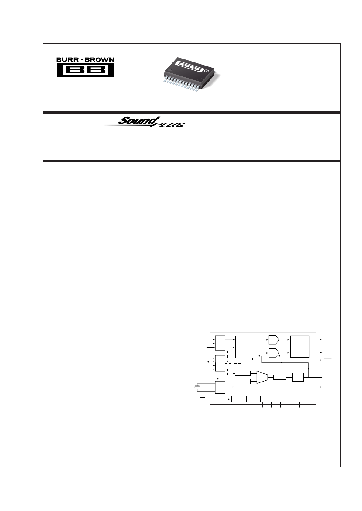
PCM1740
Stereo Audio
DIGITAL-TO-ANALOG CONVERTER
with VCXO and PLL
PCM1740
®
FEATURES
● COMPLETE DELTA-SIGMA STEREO DAC
● VOLTAGE-CONTROLLED CRYSTAL
OSCILLATOR: 27MHz ±150ppm Output with
0V to 3V Input
● PROGRAMMABLE PLL
256fS or 384fS Audio System Clock Output
● DYNAMIC PERFORMANCE:
Dynamic Range: 94dB
SNR: 94dB
THD+N: –89dB
● SAMPLING FREQUENCIES:
16kHz, 22.05kHz, 24kHz
32kHz, 44.1kHz, 48kHz
64kHz, 88.2kHz, 96kHz
● SERIAL AUDIO INTERFACE:
Standard or I2S Data Formats
16-, 20-, or 24-Bit Data
● I2C-BUS® INTERFACE FOR CONTROL
REGISTERS
(1)
:
Slave Receiver Operation
7-Bit Addressing
Standard Transfer Rate (up to 100kbps)
● PROGRAMMABLE CONTROLS:
Digital Attenuation (256 steps)
Soft Mute
Infinite Zero Detect Mute
De-Emphasis (32kHz, 44.1kHz, 48kHz)
DAC Output Mode
● SINGLE +5V SUPPLY
● SMALL SSOP-24 PACKAGE
© 2000 Burr-Brown Corporation PDS-1551A Printed in U.S.A. February, 2000
For most current data sheet and other product
information, visit www.burr-brown.com
TM
DESCRIPTION
The PCM1740 is a complete stereo audio digital-to-analog
converter with on-chip PLL and VCXO. The PCM1740 is
designed specifically for set-top box applications requiring
high-quality audio playback, a precision tuned 27MHz master clock source, and support for multiple audio-sampling
frequencies.
The stereo D/A converter utilizes multi-bit, delta-sigma
architecture, which includes an 8x interpolation filter, thirdorder noise shaping, 5-level amplitude quantization, and an
analog low-pass filter. The PCM1740 includes a number of
user-programmable functions, which are accessed via a
standard I2C-Bus interface.
APPLICATIONS
● SET-TOP BOXES
● DIGITAL BROADCAST RECEIVERS
International Airport Industrial Park • Mailing Address: PO Box 11400, Tucson, AZ 85734 • Street Address: 6730 S. Tucson Blvd., Tucson, AZ 85706 • Tel: (520) 746-1111
Twx: 910-952-1111 • Internet: http://www.burr-brown.com/ • Cable: BBRCORP • Telex: 066-6491 • FAX: (520) 889-1510 • Immediate Product Info: (800) 548-6132
NOTE: (1) I2C-Bus® is a registered trademark of Philips Semiconductor.
PCM1740
PCM
Audio
I/F
I
2
C
I/F
and
REGs
VCXO
SCL
SDA
AD1
AD0
XTUN
XT1
XT2
RST
27MHz
Crystal
8x
Oversampling
Digital Filter
and
Sub-Functions
Process
DAC
(R)
Counter N
V
OUT
L
V
COM
ZERO
SCKO
(256f
S
/384fS)
MCKO
(27MHz)
V
OUT
R
Counter M
Power Supply
Reset
BCK
LRCK
DATA
Phase
Detector
V
PP
AGND DGNDV
CC
V
DD
PGND
DAC
(L)
Low-Pass
Filter
and Amp
LPF
VCO
Page 2
®
2
PCM1740
SPECIFICATIONS
All specifications at TA = +25°C, V
CC
= V
DD
= V
PP
= 5.0V, fS = 44.1kHz, system clock = 384fS, 16-bit data, unless otherwise noted.
PCM1740E
PARAMETER CONDITIONS MIN TYP MAX UNITS
RESOLUTION 16 Bits
DATA FORMAT
Audio Interface Format Standard/ I
2
S Selectable
Audio Data Bit Length 16/20/24 Selectable Bits
Audio Data Format MSB First, Two’s Binary Complement
Sampling Frequency (f
S
) Standard (fS) 32 44.1 48 kHz
Half (fS) 16 22.05 24 kHz
Double (f
S
) 64 88.2 96 kHz
Internal System Clock Frequency 256f
S
/384f
S
DIGITAL INPUT/OUTPUT
Logic Family Input Logic TTL Compatible
High Level Input Voltage: V
IH
(1), (2)
2.0 VDC
Low Level Input Voltage: V
IL
(1), (2)
0.8 VDC
High Level Input Current: I
IH
(1), (2)
VIH = V
DD
±10 µA
Low Level Input Current:
I
IL
(1)
VIL = 0V ±10 µA
I
IL
(2)
VIL = 0V –120 µA
High Level Output Voltage: V
OH
(3)
IOH = –2mA VDD – 0.5V VDC
Low Level Output Voltage:
V
OH
(3)
IOL = 4mA 0.5 VDC
V
OL
(4)
IOL = 2mA 0.5 VDC
DIGITAL INPUT/OUTPUT of I
2
C-BUS INTERFACE
High Level Input Voltage: V
IH
(5)
3.0 V
Low Level Input Voltage: V
IL
(5)
–0.3 1.5 V
Low Level Output Voltage: V
OL
(6)
0 0.4 V
Output Fall Time: t
OF
(7)
250 ns
Input Logic Current: I
I
(8)
10% to 90% of V
DD
–10 10 µA
Capacitance for each I/O pin: C
I
(5)
10 pF
VCXO CHARACTERISTICS (MCKO) 27MHz, Fundamental Crystal
Crystal Clock Frequency
(9)
27.0000 MHz
Crystal Clock Accuracy
(9)
±30 ppm
XTUN Tuning Voltage Range
(10)
0 3.0 V
XTUN Input Impedance
(10)
60 kΩ
Output Clock Frequency XTUN = 1.3V 27.0000 MHz
Output Clock Accuracy XTUN = 1.3V ±50 ppm
VCXO Tuning Range XTUN = 0V – 3V 300 ppm
Output Clock Duty Cycle 10pF Load 35 45 55 %
Output Clock Jitter Standard Deviation 100 ps
Output Rise Time 20% to 80% V
DD
, 10pF Load 4 ns
Output Fall Time 80% to 20% V
DD
, 10pF Load 4 ns
Response Time
(11)
10 µs
Power Up Time
(12)
5ms
PLL AC CHARACTERISTICS (SCKO)
Output Clock Frequency MCKO = 27.0MHz 4.096 36.864 MHz
Output Clock Duty Cycle 10pF Load 40 50 60 %
Output Clock Jitter Standard Deviation 150 ps
Output Rise Time 20% to 80% V
DD
, 10pF Load 4 ns
Output Fall Time 80% to 20% V
DD
, 10pF Load 4 ns
Frequency Transition Time
(13)
20 ms
Power Up Time
(14)
15 30 ms
DYNAMIC PERFORMANCE
(15)
THD+N:
V
OUT
= 0dB fS = 44.1kHz 0.0035 0.01 %
fS = 96kHz 0.007 %
V
OUT
= –60dB fS = 44.1kHz 0.0035 0.01 %
f
S
= 96kHz 0.007 %
Dynamic Range f
S
= 44.1kHz, EIAJ, A-Weighted 90 94 dB
f
S
= 96kHz, A-Weighted 90 dB
Signal-to-Noise Ratio
(16)
fS = 44.1kHz, EIAJ, A-weighted 90 94 dB
f
S
= 96kHz, A-weighted 90 dB
Channel Separation f
S
= 44.1kHz 88 92 dB
f
S
= 96kHz 88 dB
Level Linearity Error V
OUT
= –90dB ±1.0 dB
Page 3
®
3
PCM1740
The information provided herein is believed to be reliable; however, BURR-BROWN assumes no responsibility for inaccuracies or omissions. BURR-BROWN assumes
no responsibility for the use of this information, and all use of such information shall be entirely at the user’s own risk. Prices and specifications are subject to change
without notice. No patent rights or licenses to any of the circuits described herein are implied or granted to any third party. BURR-BROWN does not authorize or warrant
any BURR-BROWN product for use in life support devices and/or systems.
DC ACCURACY
Gain Error ±1.0 ±3.0 % of FSR
Gain Mismatch, Channel-to-Channel ±1.0 ±3.0 % of FSR
Bipolar Zero Error ±1.0 % of FSR
ANALOG OUTPUT
Voltage Range Full Scale (0dB) 0.62 V
CC
Vp-p
Center Voltage 0.5 V
CC
VDC
Load Impedance AC Coupled 5 kΩ
DIGITAL FILTER PERFORMANCE
Passband 0.445 f
S
Hz
Stopband 0.555 f
S
Hz
Passband Ripple ±0.17 dB
Stopband Attenuation –35 dB
De-Emphasis Error –0.2 +0.55 dB
Delay Time 11.125 / f
S
sec
ANALOG FILTER PERFORMANCE
Frequency Response 20Hz to 20kHz –0.16 dB
20Hz to 40kHz –0.6 dB
POWER SUPPLY REQUIREMENTS
Voltage Range V
DD
, VCC, V
PP
+4.5 +5 +5.5 VDC
Supply Current, I
DD
+ ICC + I
PP
VDD = VCC = V
PP
= +5V 25 30 mA
Power Dissipation V
DD
= VCC = V
PP
= +5V 125 150 mW
TEMPERATURE RANGE
Operation –25 +85 °C
Storage –55 +125 °C
Thermal Resistance,
θ
JA
100 °C/W
NOTES: (1) Pins 6, 7, 18, 19: AD0, AD1, BCK, DATA, LRCK (Schmitt trigger input). (2) Pin 10: RST (Schmitt trigger input with internal pull-up resistor). (3) Pins
5, 21: MCKO, SCKO. (4) Pin 16: ZERO (open drain output). (5) Pins 8, 9: SCL, SDA. (6) Pin 9: SDA (open drain output, I
OL
= 3mA). (7) Pin 9: SDA (from V
IHMIN
to V
ILMAX
with a bus capacitance from 10pF to 400pF). (8) Pins 8, 9: SCL, SDA (input current each I/O pin with an input voltage between 0.1VDD and 0.9VDD).
(9) This characteristic is the requirement for crystal oscillator. (10) Pin 3: XTUN. (11) The maximum response time when the XTUN is changed. (12) The maximum
delay time from power on to oscillation. (13) The maximum lock up time when the PLL frequency is changed. (14) The maximum delay time from power on to lock
up. (15) Dynamic performance specifications are tested with a 20kHz low-pass filter using a Shibasoku distortion analyzer 725°C with 30kHz LPF, 400Hz HPF,
Average-Mode. (16) SNR is tested with infinite zero detection circuit disabled.
PCM1740E
PARAMETER CONDITIONS MIN TYP MAX UNITS
SPECIFICATIONS
All specifications at TA = +25°C, V
CC
= V
DD
= V
PP
= 5.0V, fS = 44.1kHz, system clock = 384fS, 16-bit data, unless otherwise noted.
Page 4
®
4
PCM1740
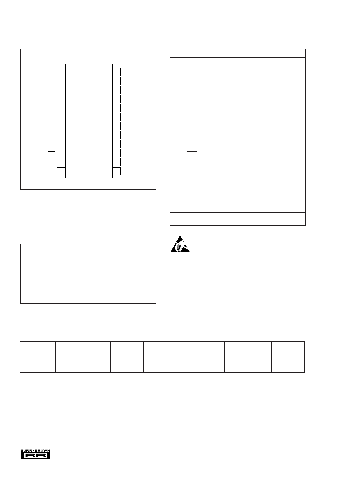
PIN NAME I/O FUNCTION
1 XT1 — 27MHz Crystal connection.
2 PGND — PLL and VCXO ground.
3 XTUN IN VCXO tune, tuning voltage range from 0V to 3V.
4V
PP
— PLL and VCXO power supply, +5V.
5 MCKO OUT Buffered clock output of VCXO.
6 AD0 IN Device address pin for I
2
C-BUS.
(1)
7 AD1 IN Device address pin for I2C-BUS.
(1)
8 SCL IN Bit clock input for I2C-BUS interface.
9 SDA
IN/OUT
Serial data for I2C-BUS interface.
10 RST IN Reset, active LOW.
(2)
11 V
OUT
R OUT Right-channel analog voltage output.
12 AGND — Analog ground.
13 V
CC
— Analog power supply, +5V.
14 V
OUT
L OUT Left-channel analog voltage output.
15 V
COM
— DC common-mode voltage output.
16 ZERO OUT Zero flag output, active LOW.
(3)
17 BCK IN Bit clock input for serial audio data.
(1)
18 DATA IN Serial audio data input.
(1)
19 LRCK IN Left and right word clock, equal to the sampling
rate (f
S
).
(1)
20 RSV — Reserved must be open.
21 SCKO OUT System clock output, 256/384 f
S
.
22 V
DD
— Digital power supply, +5V.
23 DGND — Digital ground.
24 XT2 — 27MHz Crystal connection.
NOTES: (1) Schmitt trigger input. (2) Schmitt trigger input with internal
pull-up resistor. (3) Open drain output.
Power Supply Voltage
(1)
...................................................................+6.5V
Supply Voltage Differences
(2)
........................................................... ±0.1V
GND Voltage Differences
(3)
.............................................................. ±0.1V
Digital Input Voltage................................................. –0.3V to (V
DD
+ 0.3V)
Analog Input Voltage................................................–0.3V to (V
CC
+ 0.3V)
Input Current (any pins except supplies) ........................................ ±10mA
Operating Temperature Range ......................................... –25°C to +85°C
Storage Temperature...................................................... –55°C to +125°C
Junction Temperature .................................................................... +150°C
Lead Temperature (soldering, 5s).................................................. +260°C
Package Temperature (IR reflow, peak, 10s) ................................ +235°C
NOTES: (1) V
CC
, VDD, VPP. (2) Among VCC, VDD, VPP. (3) Among AGND, DGND,
and PGND. Stresses above those listed under Absolute Maximum Ratings may
cause permanent damage to the device. Exposure to absolute maximum
conditions for extended periods may affect device reliability.
PIN ASSIGNMENTSPIN CONFIGURATION
Top View SSOP
ABSOLUTE MAXIMUM RATINGS
ELECTROSTATIC
DISCHARGE SENSITIVITY
This integrated circuit can be damaged by ESD. Burr-Brown
recommends that all integrated circuits be handled with
appropriate precautions. Failure to observe proper handling
and installation procedures can cause damage.
ESD damage can range from subtle performance degradation
to complete device failure. Precision integrated circuits may
be more susceptible to damage because very small parametric
changes could cause the device not to meet its published
specifications.
PACKAGE SPECIFIED
DRAWING TEMPERATURE PACKAGE ORDERING TRANSPORT
PRODUCT PACKAGE NUMBER RANGE MARKING NUMBER
(1)
MEDIA
PCM1740E SSOP-24 338 –25°C to +85°C PCM1740E PCM1740E Rails
" " " " PCM1740E PCM1740E/2K Tape and Reel
NOTE: (1) Models with a slash (/) are available only in Tape and Reel in the quantities indicated (e.g., /2K indicates 2000 devices per reel). Ordering 2000 pieces
of “PCM1740E/2K” will get a single 2000-piece Tape and Reel.
PACKAGE/ORDERING INFORMATION
XT1
PGND
XTUN
V
PP
MCKO
AD0
AD1
SCL
SDA
RST
V
OUT
R
AGND
PCM1740
XT2
DGND
V
DD
SCKO
RSV
LRCK
DATA
BCK
ZERO
V
COM
V
OUT
L
V
CC
1
2
3
4
5
6
7
8
9
10
11
12
24
23
22
21
20
19
18
17
16
15
14
13
Page 5

®
5
PCM1740
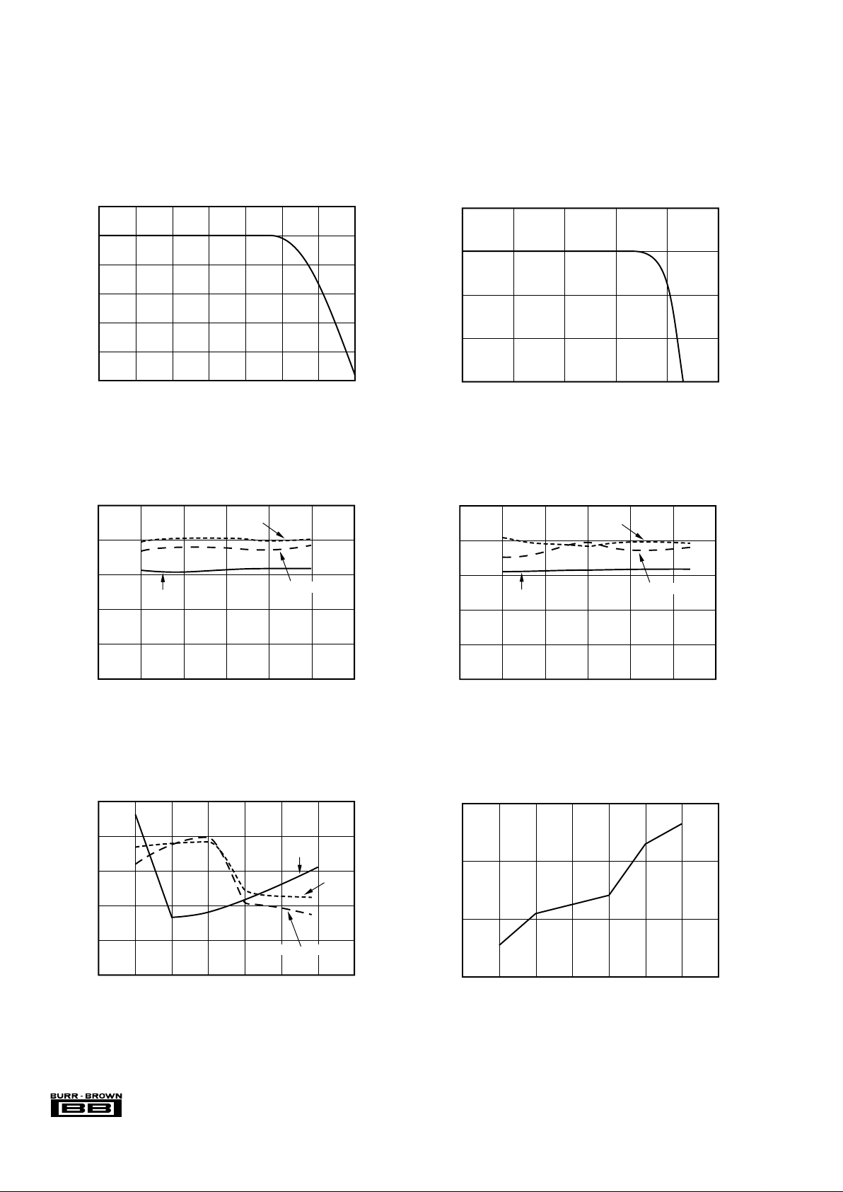
TYPICAL PERFORMANCE CURVES
At TA = +25°C, VCC = VDD = +5V, fS = 44.1kHz, F
SCKO
= 384fS = 16.9344MHz, and 16-bit data, unless otherwise noted.
FREQUENCY RESPONSE
(De-emphasis OFF, f
S
= 44.1kHz)
f
S
Level (dB)
0
–20
–40
–60
–80
–100
01234
PASSBAND RIPPLE
(De-emphasis OFF, f
S
= 44.1kHz)
f
S
Level (dB)
0
–0.2
–0.4
–0.6
–0.8
–1
0 0.20.1 0.3 0.4 0.5
DE-EMPHASIS FREQUENCY RESPONSE (3kHz)
0 5k 10k 15k 20k 25k
Frequency (Hz)
0
–2
–4
–6
–8
–10
–12
DE-EMPHASIS FREQUENCY RESPONSE (44.1kHz)
0 5k 10k 15k 20k 25k
Frequency (Hz)
0
–2
–4
–6
–8
–10
–12
DE-EMPHASIS FREQUENCY RESPONSE (48kHz)
0 5k 10k 15k 20k 25k
Frequency (Hz)
0
–2
–4
–6
–8
–10
–12
Level (dB) Level (dB) Level (dB)
DE-EMPHASIS ERROR (3kHz)
0 3628 7256 10884 14512
0 4999.8375 9999.675 14999.5125 19999.35
0 5442 10884 16326 21768
Frequency (Hz)
0.6
0.4
0.2
0
–0.2
–0.4
–0.6
0.6
0.4
0.2
0
–0.2
–0.4
–0.6
0.6
0.4
0.2
0
–0.2
–0.4
–0.6
DE-EMPHASIS ERROR (44.1kHz)
Frequency (Hz)
DE-EMPHASIS ERROR (48kHz)
Frequency (Hz)
Error (dB) Error (dB) Error (dB)
Page 6
®
6
PCM1740
TYPICAL PERFORMANCE CURVES (Cont.)
At TA = +25°C, VCC = VDD = +5V, fS = 44.1kHz, F
SCKO
= 384fS = 16.9344MHz, and 16-bit data, unless otherwise noted.
ANALOG FILTER
(1Hz to 10MHz)
Log Frequency (Hz)
Level (dB)
20
0
–20
–40
–60
–80
–100
0 0.20.1 0.1 0.3 0.40.4 0.5
ANALOG FILTER
(1Hz to 20kHz)
Log Frequency (Hz)
Level (dB)
0.05
0
–0.05
–0.1
–0.15
110 1k100 10k 100k
SUPPLY CURRENT vs SAMPLING FREQUENCY
Sampling Frequency (kHz)
Supply Current (mA)
35
30
25
20
32 64 88.244.1 48 96.0
THD+N (FS), DYNAMIC RANGE, and SNR
vs SUPPLY VOLTAGE
(Temperature = 25°C, 384f
S
, fS = 44.1kHz)
Supply Voltage (V)
THD+D (FS) (%)
0.005
0.004
0.003
0.002
0.001
0.000
Dynamic Range, SNR (dB)
95
94
93
92
91
90
4.25 4.5 5.254.75 5 5.5 5.75
SNR
THD+N
Dynamic Range
THD+N (FS), DYNAMIC RANGE, and SNR
vs TEMPERATURE
(V
CC
= VDD = VPP = 5V, 384fS, fS = 44.1kHz)
Temperature (°C)
THD+D (FS) (%)
0.005
0.004
0.003
0.002
0.001
0.000
Dynamic Range, SNR (dB)
95
94
93
92
91
90
–50 –25 500 25 75 100
SNR
THD+N
Dynamic Range
THD+N (FS), DYNAMIC RANGE, and SNR
vs SAMPLING FREQUENCY
Sampling Frequency (kHz)
THD+D (FS) (%)
0.010
0.008
0.006
0.004
0.002
0.000
Dynamic Range, SNR (dB)
96
94
92
90
88
86
32 64 88.244.1 48 96.0
SNR
THD+N
Dynamic Range
Page 7

®
7
PCM1740
3rd ORDER ∆Σ MODULATOR
Frequency (kHz)
Gain (–dB)
20
0
–20
–40
–60
–80
–100
–120
–140
–160
0 5 10 15 20 25
STEREO DIGITAL-TO-ANALOG
CONVERTER
The stereo D/A converters of the PCM1740 utilize a multilevel delta-sigma architecture. Based upon a third-order
noise shaper and a 5-level amplitude quantizer, this section
converts the 8x oversampled, 18-bit input data from the
interpolation filter to a 5-level delta-sigma format. A block
diagram of the multi-level delta-sigma modulator is shown
in Figure 1. This architecture has the advantage of improved
stability and increased tolerance to clock jitter when compared to the one-bit (2-level) delta-sigma D/A converters.
The combined oversampling rate of the delta-sigma modulator and the 8x interpolation filter is 48fS for a 384fS system
clock, and 64fS for a 256fS system clock. The theoretical
quantization noise performance for the 5-level delta-sigma
modulator is shown in Figure 2.
The output of the delta-sigma modulator is low-pass filtered
and buffered by an on-chip output amplifier. For best
performance, an external low-pass filter is recommended.
Refer to the “Applications Information” section of this data
sheet for details regarding DAC output filter recommendations.
The PCM1740 includes two analog outputs, V
OUT
L (pin 14)
and V
OUT
R (pin 11), corresponding to the left and right
audio outputs. The full-scale output amplitude is 0.62 • VCC,
or 3.1Vp-p with a +5V supply and an AC coupled load of
5kΩ or greater. The analog outputs are centered about the
DC common mode voltage, which is typically VCC/2.
The DC common-mode voltage is made available at the
V
COM
output (pin 15). This is an unbuffered output, prima-
Out
48f
S
(384fS)
64f
S
(256fS)
In
8f
S
18-Bit
+
++
4
3
2
1
0
5-level Quantizer
+
–
+
Z
–1
+
–
+
Z
–1
+
+
Z
–1
FIGURE 2. Quantization Noise Spectrum.
rily used for de-coupling purposes. See the “Applications
Information” section of this data sheet for more information
regarding the use of the V
COM
output for biasing external
circuitry.
VOLTAGE CONTROLLED CRYSTAL OSCILLATOR
(VCXO)
The PCM1740 includes an on-chip voltage-controlled crystal oscillator, or VCXO, which is used to generate the
27MHz master clock required by most digital broadcast and
MPEG-2 decoding applications.
FIGURE 1. 5-Level ∆Σ Modulator Block Diagram.
Page 8

®
8
PCM1740
The 27MHz clock is available at the MCKO output (pin 5).
The VCXO output frequency can be precisely tuned using a
control voltage at the XTUN input (pin 3). The tuning range
is 27MHz ±150ppm typical for a 0V to +3V control voltage
range. Figure 3 shows the VCXO equivalent circuit, while
Figure 4 shows the typical tuning curve.
At power up, the VCXO requires 5ms start up time. The
VCXO also exhibits a 10µs settling time in response to
changes in the XTUN control voltage. VCXO operation and
the MCKO output are not effected by the power on or
external reset functions, continuing to operate during the
initialization sequence.
Crystal Selection
The VCXO connects to an external 27MHz crystal via XT1
(pin 1) and XT2 (pin 24). The crystal should be AT-cut,
fundamental mode with ±30ppm accuracy and less than 50Ω
motional resistance. Crystal shunt capacitance should be 3pF
maximum, while load capacitance should be less than 7pF.
Miniature lead type or surface-mount devices are recommended. External load capacitors are not needed, since they
are provided on-chip. The crystal should be placed as close as
possible to the XT1 and XT2 pins to reduce effects of parasitic
capacitance and land resistance.
PROGRAMMABLE PHASE LOCKED LOOP (PLL)
The PCM1740 includes an on-chip PLL for generating a 256f
S
or 384fS audio system clock from the 27MHz VCXO output.
A block diagram of the PLL section is shown in Figure 5. The
PLL output clock is used by the digital filter and delta-sigma
modulator circuitry, and is made available at the SCKO output
(pin 21) for use with additional audio converters and signal
processors.
Tuning Voltage (V)
VCXO Output Frequency (MHz)
27.005
27.004
27.003
27.002
27.001
27.000
26.999
26.998
26.997
26.996
26.995
0.0 0.5 1.51.0 2.0 2.5 3.0 3.5 4.0
27MHz
Crystal
XTUN
0V to +3V
VCXO
MCKO
27MHz ±150ppm
SCKO
256/384f
S
Frequency
Selection
ROM
Phase
Detector
and
Loop Filter
PLL
N Counter
Frequency Selection
Control Register 3
VCO
M Counter
FIGURE 3. VCXO Equivalent Circuit.
FIGURE 4. VCXO Output Frequency (MCKO) versus
Tuning Voltage (XTUN).
XT1
27MHz
Crystal
27MHz
Tuned Clock
Voltage
Range
0 to 3V
1
24
3
XTUN
C
LV
XT2
C
L
FIGURE 5. PLL Block Diagram.
Page 9

®
9
PCM1740
The PLL can generate one of nine pre-programmed system
clock rates for either 256fS or 384fS output. The PLL output
and sampling frequencies are programmed using Control
Register 3. Table I shows the available sampling frequencies
and the corresponding PLL output clock rates. The reset
default condition for the PLL is fS = 44.1kHz with SCKO =
384fS, or 16.9344MHz.
At power up, the PLL requires 30ms start up time for
stabilization. The PLL also exhibits a settling time of 20ms
in response to changes in sampling frequency selection.
The PLL output continues to operate during power on or
external reset sequences, with the sampling frequency set to
fS = 44.1kHz and SCKO = 384fS.
RESET OPERATION
POWER ON RESET
The PCM1740 includes power-on reset circuitry for start up
initialization. The initialization sequence starts when V
DD
exceeds 2.2V (typical). The initialization sequence requires
1024 PLL output (or SCKO) clock cycles for completion.
During initialization, both V
OUT
L and V
OUT
R are forced to
VCC/ 2. Figure 6 shows the power on reset timing, while
Table II shows the reset default settings for user-programmable functions. The user should not attempt to write
control registers via the I2C-Bus interface during the initialization sequence.
EXTERNAL RESET
The PCM1740 includes an external reset input, RST (pin
10). This input may be used to force an initialization sequence. As shown in Figure 7, the RST pin must be held low
for a minimum of 20ns. The initialization sequence will then
start on the rising edge of RST. Initialization requires 1024
PLL output (or SCKO) clock cycles for completion. During
initialization, both V
OUT
L and V
OUT
R are forced to VCC/2.
Table II shows the reset default settings for user-programmable functions. The user should not attempt to write
control registers via the I2C-Bus interface during the initialization sequence.
SAMPLING INTERNAL SYSTEM INTERNAL SYSTEM
FREQUENCY (LRCK) Clock - 256f
S
Clock - 384f
S
16kHz Half 4.096MHz 6.144MHz
32kHz Normal 8.192MHz 12.288MHz
64kHz Double 16.384MHz 24.576MHz
22.05kHz Half 5.6448MHz 8.4672MHz
44.1kHz Normal 11.2896MHz 16.9344MHz
88.2kHz Double 22.5792MHz 33.8688MHz
24kHz Half 6.144MHz 9.216MHz
48kHz Normal 12.288MHz 18.432MHz
96kHz Double 24.576MHz 36.864MHz
TABLE I. PLL Sampling and System Clock Frequencies.
1024 System Clock Periods
Reset
Reset Removal
2.4V
2.2V
2.0V
VCC/V
DD
Internal Reset
System Clock
(SCKO)
1024 System Clock Periods
Reset
Reset Removal
System Clock
(SCKO)
Internal Reset
RST
t
RST
t
RST
t
RST
≥ 20ns
FIGURE 6. Power-On Reset Operation.
FIGURE 7. External Reset Operation.
Page 10

®
10
PCM1740
LRCK
BCK
DATA
SCKO
Frame Sync
Serial Bit Clock
Serial Data Output
Audio Clock
PCM1740Audio DSP/Decoder
14 15 16 1 2 3
14 15
1/fs
L_ch
R_ch
MSB LSB
16
LRCIN (pin 4)
(a) Standard Right - Justified Format
(b) I
2
S Format
BCKIN (pin 6)
AUDIO DATA WORD = 16-BIT
DIN (pin 5)
1 2 3
14 15
MSB LSB
16
18 19 20 1 2 3
18 19
MSB LSB
20
AUDIO DATA WORD = 20-BIT
DIN (pin 5)
1 2 3
18 19
MSB LSB
20
23 24 1 2 3
22 23
MSB LSB
24
AUDIO DATA WORD = 24-BIT
DIN (pin 5)
1 2 3
22 23
MSB LSB
24
1 2 3
14 15
1/fs
L_ch
R_ch
MSB LSB
16
LRCIN (pin 4)
BCKIN (pin 6)
AUDIO DATA WORD = 16-BIT
DIN (pin 5)
1 2 3
14 15
MSB LSB
16
1 2 3
18 19
MSB LSB
20
AUDIO DATA WORD = 20-BIT
DIN (pin 5)
1 2 3
18 19
MSB LSB
20
21
21
21
1 2 3
22 23
MSB LSB
24
AUDIO DATA WORD = 24-BIT
DIN (pin 5)
1 2 3
22 23
MSB LSB
24
The LRCK input is operated at the sampling frequency, fS.
The BCK input is operated at 32, 48, or 64 times the
sampling frequency. Both LRCK and BCK must be synchronous with the SCKO output for proper operation.
Data Formats
The PCM1740 supports two audio interface formats: Standard and I2S. These formats are shown in Figure 9. The
audio data word length for the Left and Right channels may
be 16-, 20-, or 24-bits. The audio data word length and
format are programmed using Control Registers 2 and 3. The
reset default condition is Standard format with 16-bit audio
data.
Timing Requirements
Figure 10 shows the audio interface timing requirements.
ZERO FLAG OUTPUT
The PCM1740 includes a zero flag output, ZERO (pin 16).
This is an open-drain output, and a 10kΩ pull-up resistor
connected to VDD is recommended when using the ZERO
flag as a logic output.
The PCM1740 includes an infinite zero detection function
that monitors the audio data at the DATA input (pin 18). If
the audio data for both the left and right channels is all zeros
for 65,536 continuous BCK clock cycles, the zero flag will
be activated, turning on a MOSFET switch and connecting
the ZERO pin to ground. This provides an active low output
that may be used to control an external mute circuit, or as a
logic indicator for an audio DSP/decoder or microprocessor.
AUDIO SERIAL INTERFACE
The PCM1740 includes a three-wire serial audio interface.
This includes LRCK (pin 19), BCK (pin 17), and DATA
(pin 18). The LRCK input is the audio left/right clock, which
is used as a latch signal for the interface. The BCK input is
used to clock audio data into the serial port. The DATA
input carries multiplexed data for the left and right audio
channels. Audio data must be Two’s Complement, MSB
first formatted. Figure 8 shows the typical connection between the PCM1740 audio serial interface and an audio DSP
or decoder.
LRCK and BCK Rates
FIGURE 8. Interfacing the PCM1740 to an Audio DSP.
FIGURE 9. Audio Interface Formats.
Page 11

®
11
PCM1740
Loss of Synchronization
Ideally, LRCK and BCK will be derived from the SCKO
output, ensuring synchronous operation. For other cases, the
PCM1740 includes circuitry to detect loss of synchronization between the LRCK and the system clock, SCKO. A loss
of synchronization condition is detected when the phase
relationship between SCKO and LRCK exceeds ±6 BCK
cycles during one sample period, or 1/fS. If a loss of
synchronization condition is detected, the DAC operation
will halt within one sample period and the analog outputs
will be forced to VCC/ 2 until re-synchronization between
LRCK and SCKO is completed. Figure 11 shows the state of
the analog outputs given a loss of synchronization event.
During the undefined states, as well as transitions between
normal and undefined states, the analog outputs may generate audible noise.
USER PROGRAMMABLE FUNCTIONS
The PCM1740 includes a number of programmable functions, which are configured using five control registers.
These registers are accessed using the I2C-Bus interface.
This section describes the control registers, while the
I2C-Bus interface is described in a later section. Table II lists
the available functions and their corresponding reset default
condition.
Register Map
The control register map is shown in Table III. Sub-address
bits B8 through B10 are used to specify the register that is
being written. All reserved bits, shown as “res”, must be set
to ‘0’.
Register Descriptions
The following pages provide detailed descriptions of the five
control registers and their associated functions. All reserved
bits, shown as “res”, must be set to ‘0’.
FIGURE 10. Audio Interface Timing.
FIGURE 11. Loss of Synchronization and Analog Output State.
REGISTER B15 B14 B13 B12 B11 B10 B9 B8 B7 B6 B5 B4 B3 B2 B1 B0
Register 0 res res res res res A2 A1 A0 AL7 AL6 AL5 AL4 AL3 AL2 AL1 AL0
Register 1 res res res res res A2 A1 A0 AR7 AR6 AR5 AR4 AR3 AR2 AR1 AR0
Register 2 res res res res res A2 A1 A0 PL3 PL2 PL1 PL0 IW1 IW0 DEM MUT
Register 3 res res res res res A2 A1 A0 SF1 SF0 DSR1 DSR0 SYS ATC LRP IIS
Register 4 res res res res res A2 A1 A0 res res res res res OPE IZD LD
SUB ADDRESS BYTE
DATA BYTE
TABLE III. Control Register Map.
FUNCTION MODE BY DEFAULT
Audio Data Format Select:
Standard Format/I
2
S Format Standard Format
Audio Data Word Select:
16-Bit/20-Bit/24-Bit 16-Bit
Polarity of LR-clock Selection Left/Right = HIGH/LOW
De-emphasis Control:
OFF, 32kHz, 44.1kHz, 48kHz OFF
Soft Mute Control OFF
Attenuation Data for Left-channel 0dB
Attenuation Data for Right-channel 0dB
Attenuation Data Mode Control Left-channel, Right-channel Individually
Analog Output Mode Select Stereo Mode
Infinity Zero Detect Mute Control OFF
DACs Operation Control ON
System Clock Select: 256f
S
/384f
S
384f
S
Sampling Frequency Select:
32kHz Group, 44.1kHz Group, 48kHz Group 44.1kHz Group
Sampling Frequency Multiplier:
Normal/Double/ Half Normal, x1
TABLE II. User-Programmable Functions.
Normal Normal
Synchronous Asynchronous
within
1/f
S
Synchronous
Undefined Data
Undefined
Data
V
COM
(= 0.5 VCC)
22.2/f
S
State of
Synchronization
V
OUT
LRCKIN
BCKIN
DIN
1.4V
1.4V
1.4V
t
BCH
t
BCL
t
LB
t
BL
t
DS
BCKIN Pulse Cycle Time
BCKIN Pulse Width High
BCKIN Pulse Width Low
BCKIN Rising Edge to LRCIN Edge
LRCIN Edge to BCKIN Rising Edge
DIN Set-up Time
DIN Hold Time
: t
BCY
: t
BCH
: t
BCL
: t
BL
: t
LB
: t
DS
: t
DH
: 100ns (min)
: 50ns (min)
: 50ns (min)
: 30ns (min)
: 30ns (min)
: 30ns (min)
: 30ns (min)
t
DH
t
BCY
Page 12

®
12
PCM1740
REGISTER DEFINITIONS
B15 B14 B13 B12 B11 B10 B9 B8 B7 B6 B5 B4 B3 B2 B1 B0
Register 0 res res res res res 0 0 0 AL7 AL6 AL5 AL4 AL3 AL2 AL1 AL0
Left Channel Attenuation Data
Default: AL[7:0] = FF
HEX
Register 0 is used to set the digital attenuation level for the Left Channel. If the ATC bit in Register 3 is set to “1”, then this
data is also used to control the Right Channel attenuation. The attenuation level is defined by the following relationships:
Attenuation (dB) = 20 x log (AL[7:0]
DEC
÷ 256), when AL[7:0] = 01
HEX
(1
DEC
) through FE
HEX
(254
DEC
)
Attenuation (dB) = –∞ (or Mute), when AL[7:0] = 00
HEX
Attenuation (dB) = 0dB, when AL[7:0] = FF
HEX
The Attenuation Load bit, LD, in Register 4 must be set to “1” in order to update attenuation settings.
If LD is set to “0”, the attenuation remains at the previously programmed level, ignoring the new data until LD is set to “1”.
B15 B14 B13 B12 B11 B10 B9 B8 B7 B6 B5 B4 B3 B2 B1 B0
Register 1 res res res res res 0 0 1 AR7 AR6 AR5 AR4 AR3 AR2 AR1 AR0
Right Channel Attenuation Data
Default: AR[7:0] = FF
HEX
Register 1 is used to set the digital attenuation level for the Right Channel. If the ATC bit in Register 3 is set to ‘1’, then the
Left Channel attenuation data in Register 1 is used to control the Right Channel attenuation. The attenuation level is defined
by the following relationships:
Attenuation (dB) = 20 x log (AR[7:0]
DEC
÷ 256), when AR[7:0] = 01
HEX
(1
DEC
) through FE
HEX
(254
DEC
)
Attenuation (dB) = –∞ (or Mute), when AR[7:0] = 00
HEX
Attenuation (dB) = 0dB, when AR[7:0] = FF
HEX
The Attenuation Load bit, LD, in Register 4 must be set to 1 in order to update attenuation settings.
If LD is set to “0”, the attenuation remains at the previously programmed level, ignoring the new data until LD is set to “1”.
MUT Soft Mute Control
The MUT bit controls the soft mute function. Soft mute changes the digital attenuation level for both the Left
and Right channels, stepping from the currently programmed value to infinite attenuation one step per sample
period, or 1/fS. This provides a quiet muting of the outputs without audible noise.
MUT = 0 Soft Mute Disabled (default)
MUT = 1 Soft Mute Enabled
DEM Digital De-Emphasis
The DEM bit controls the digital de-emphasis function, which is valid only for 32kHz, 44.1kHz,
and 48kHz sampling frequencies. The de-emphasis plots are shown in the Typical Performance Curves section
of this data sheet.
DEM = 0 De-Emphasis OFF (default)
DEM = 1 De-Emphasis ON
B15 B14 B13 B12 B11 B10 B9 B8 B7 B6 B5 B4 B3 B2 B1 B0
Register 2 res res res res res 0 1 0 PL3 PL2 PL1 PL0 IW1 IW0 DEM MUT
Page 13

®
13
PCM1740
IW0 Audio Data Word Length
IW1
The IW0 and IW1 bits are used to select the data word length for the audio serial interface.
The audio data format is selected using the IIS bit in Register 3.
IW1 IW0 Word Length
0 0 16-bits (default)
0 1 20-bits
1 0 24-bits
1 1 Reserved
PL[3:0] Analog Output Mode Select
Bits PL[3:0] are used to set the output mode for the analog outputs. Refer to the table below.
PL3 PL2 PL1 PL0 V
OUT
LV
OUT
R Notes
0 0 0 0 Mute Mute Mute
0 0 0 1 Left Mute
0 0 1 0 Right Mute
0 0 1 1 (L+R)/ 2 Mute
0 1 0 0 Mute Left
0 1 0 1 Left Left
0 1 1 0 Right Left Reverse
0 1 1 1 (L+R)/ 2 Left
1 0 0 0 Mute Right
1 0 0 1 Left Right Stereo (default)
1 0 1 0 Right Right
1 0 1 1 (L+R)/ 2 Right
1 1 0 0 Mute (L+R)/2
1 1 0 1 Left (L+R)/ 2
1 1 1 0 Right (L+R)/2
1 1 1 1 (L+R)/ 2 (L+R)/2 Mono
IIS Audio Data Format
The IIS bit is used to select the audio data format, either Standard Right Justified or I2S.
IIS = 0 Standard Right Justified (default)
IIS = 1 I2S
LRP LRCK Polarity
The LRP bit selects the polarity of left/right clock input (LRCK) when using the Standard Right Justified audio
data format. This bit has no effect when using the I2S audio data format.
LRP = 0 Left Channel when LRCK = High; Right Channel when LRCK = Low (default)
LRP = 1 Left Channel when LRCK = Low; Right Channel when LRCK = High
ATC Attenuation Mode Control
The ATC bit is used to select independent or common attenuation data for the Left and Right channels.
ATC = 0 Independent: Left Channel uses Register 0 and Right Channel uses Register 1 (default)
ATC = 1 Common: Left and Right Channels both use Register 0
B15 B14 B13 B12 B11 B10 B9 B8 B7 B6 B5 B4 B3 B2 B1 B0
Register 3 res res res res res 0 1 1 SF1 SF0 DSR1 DSR0 SYS ATC LRP IIS
Page 14

®
14
PCM1740
SYS Audio System Clock (or SCKO)
The SYS bit is used to select the system clock (or SCKO) frequency, either 256fS or 384fS.
SYS = 0 384fS (default)
SYS = 1 256f
S
DSR0 Sampling Frequency Multiplier
DSR1
The DSR0 and DSR1 bits are used to select the multiplier used in conjunction with the SF0 and SF1 bits.
DSR1 DSR0 Multiplier
0 0 Normal, x1 (default)
0 1 Double, x2
1 0 Half, x 1/ 2
1 1 Reserved
SF0 Sampling Frequency Select
SF1
The SF0 and SF1 bits are used to select the sampling frequency group (32kHz, 44.1kHz, or 48kHz). The DSR0
and DSR1 bits, described previously, are used to select the multiplier.
SF1 SF0 Sampling Frequency Group
0 0 44.1kHz Group ( 22.05kHz, 44.1kHz, or 88.2kHz) (default)
0 1 48 kHz Group (24kHz, 48kHz, or 96kHz)
1 0 32 kHz Group (16kHz, 32kHz, or 64kHz)
1 1 Reserved
LD Attenuation Data Load Control
The LD bit is used to simultaneously set the Left and Right digital attenuation data. When LD is set to “1”, the
digital attenuation data given by Registers 0 and 1 is loaded for the Left and Right channels. When LD is set
to “0”, updates to Registers 0 and 1 are ignored, and the attenuation settings remain as previously programmed
until LD is set to “1”.
LD = 0 Disabled
LD = 1 Enabled: Left and Right Attenuation Data Updated Simultaneously
IZD Infinite Zero Detect Mute
The IZD bit is used to enable/disable the infinite zero detect mute function. The PCM1740 includes infinite zero
detection logic that monitors the audio data at the DATA input (pin 18). If the audio data for both the Left and
Right channels is all zeros for 65,536 continuous BCK clock cycles, the zero flag will be activated and output
amplifier will be disconnected from the output of the delta-sigma modulator. The output amplifier’s input is
switched to the DC common mode voltage. This forces V
OUT
L and V
OUT
R to VCC/2. The ZERO output flag (pin
16) is not affected by the setting of this bit.
IZD = 0 Disabled (default)
IZD = 1 Enabled
OPE DAC Operation Control
The OPE bit is used to enable/disable the operation of the D/A converters. When enabled, the DAC outputs are
connected to the output amplifier for normal operation. When disabled, the output amplifier is disconnected from
the DAC output and switched to the DC common mode voltage. This forces V
OUT
L and V
OUT
R to VCC/2.
OPE = 0 Enabled: Normal Operation(default)
OPE = 1 Disabled: Outputs forced to VCC/2
B15 B14 B13 B12 B11 B10 B9 B8 B7 B6 B5 B4 B3 B2 B1 B0
Register 4 res res res res res 1 0 0 res res res res res OPE IZD LD
Page 15

®
15
PCM1740
I2C-BUS INTERFACE DESCRIPTION
The PCM1740 includes an I2C-Bus interface for writing the
internal control registers. This provides an industry standard
method for interfacing a host CPU control port to the
PCM1740. The PCM1740 operates as a Slave receiver on
the bus, and supports data transfer rates up to 100 kilobitsper-second (kbps).
The I2C-Bus interface is comprised of four signals: SDA
(pin 9), SCL (pin 8), AD0 (pin 6), and AD1 (pin 7). The SCL
input is the serial data clock, while SDA is the serial data
input. SDA carries start/stop, slave address, sub-address (or
register address), register, and acknowledgment data. The
AD0 and AD1 inputs form the lower two bits of the slave
address.
Slave Address
The PCM1740 Slave address consists of seven bits, as shown
in Figure 12. The five most significant bits are fixed, while the
two least significant bits, named A0 and A1, are defined by the
logic levels present at the AD0 and AD1 input pins. This
allows four PCM1740’s to reside on the same I2C-Bus.
Bus Operation
Figure 13 shows the typical configuration of the PCM1740 on
the I2C-Bus. The Master transmitter or transmitter/receiver is
typically a microcontroller, or an audio DSP/decoder. The
Master device controls the data transfers on the bus. The
PCM1740 operates as a Slave receiver, and accepts data from
the Master when it is properly addressed. The data transfer
may be comprised of an unlimited number of bytes, or 8-bit
data words. Figure 14 shows the message transfer protocol.
For normal bit transfer on the bus, data on SDA must
be static while SCL is High. Data on SDA may change
High / Low states when SCL is Low. The exception to this
rule is the Start and Stop conditions.
The Start condition is defined by a High-to-Low transition on
SDA while SCL is High, and is denoted with an “S” in Figure
12. The Stop condition is defined by a Low-to-High transition
on SDA while SCL is High, and is denoted with a “P” in
Figure 12. The Start and Stop conditions are always generated
by the Master. All data transfers from Master to Slave begin
with a Start condition and end with a Stop condition. The bus
is considered to be busy after the Start condition, and becomes
free some time after the Stop condition.
Master
Transmitter/
Receiver
SCL
SDA
Slave
Receiver
(PCM1740)
Slave
Transmitter/
Receiver
Master
Transmitter/
Receiver
SDA
SCL
Start
Condition
Start
Condition
StopAddress AddressR/W R/WACK ACKACKData
1-7 1-78 89 9981-7
NOTES: (1) Clock LOW (min) = 4.7µs; clock HIGH (min) = 4µs. (2) The dased line is the
acknoweledgement of the receiver. (3) Mark-to space ratio = 1:1 (LOW-to-HIGH). (4) Maximum
number of bytes is unrestriced. (5) Premature termination of transfer is allowed by generation of
STOP condition. (6) Acknowledge clock bit must be provided by master.
FIGURE 12. Control Data Format.
FIGURE 13. Typical I2C-Bus Configuration.
FIGURE 14. I2C Bus Data Transfer.
01
Slave Address
1A1A0S10 0
MSB R/W
A B12 B11 B10B15 B14 B13 B09 B08 A B07 B06
B02 B01 B00B05 B04 B03
A
Internal Strobe for
Data Latching
Not Acknowledge
P
Acknowledge
from
Slave
Acknowledge
from
Slave
Start
from
Master
Stop
from
Master
Sub Address Byte Data Byte
Page 16

®
16
PCM1740
Data transfer begins with a Start condition, and is immediately followed by the Slave address and Read/Write bit. The
Read / Write bit is set to “0” for the PCM1740, in order to
write data to the control register specified by the subaddress. This is followed by an acknowledgment from the
PCM1740, the sub-address (i.e., control register address),
another acknowledgment from the PCM1740, the control
register data, and another acknowledgment from the
PCM1740. What happens after this depends upon if the user
wants to continue writing additional control registers, or if
they want to terminate the data transfer. If the user wants to
continue, the acknowledgment is followed by a Start condi-
tion for the next write sequence. If the user decides to
terminate the data transfer, then a Stop condition is generated by the Master.
The I2C-Bus specification defines timing requirements for
devices connected to the bus. Timing requirements for the
PCM1740 are shown in Figure 15.
Reference
For additional information regarding the I2C-Bus, please
refer to the I2C-Bus Specification, Version 2.0, published in
December 1998 by Philips Semiconductors.
FIGURE 15. I2C Bus Timing.
SDA
SCL
S: START condition
Sr: repeated START condition
P: STOP condition
t
F
t
HD; STA
S Sr P S
t
HD; DAT
t
HIGH
t
SU; STA
t
SU; STO
t
R
t
HD; STA
t
R
t
LOW
t
F
t
SU, DAT
t
BUF
SYMBOL DESCRIPTION MIN TYP MAX UNITS
f
SCL
SCL Clock Frequency 100 kHz
t
HD; STA
Hold time (repeated) START condition, 4.0 µs
after this period, the first clock pulse is
generated
t
LOW
LOW period of the SCL clock 4.7 µs
t
HIGH
HIGH period of the SCL clock 4.0 µs
t
SU:STA
Set-up time for a repeated START condition
4.7 µs
t
HD;DAT
Data hold time for I2C-BUS devices 0 3.45(2) µs
t
SU;DAT
Data set-up time 250 ns
t
R
Rise time of both SDA and SCL signals 1000 ns
t
F
Fall time of both SDA and SCL signals 300 ns
t
SU;STO
Set-up time for STOP condition 4.0 µs
t
BUF
Bus free time between a STOP and START
4.7 µs
condition
C
B
Capacitive load for each bus line 400 pF
V
NL
Noise margin at the LOW level for each 0.1 V
DD
V
connected device (including hysteresis)
V
NH
Noise margin at the HIGH level for each 0.2 V
DD
V
connected device (including hysteresis)
Page 17

®
17
PCM1740
FIGURE 16. Basic Connection Diagram.
+
+
XT1
PGND
XTUN
V
PP
MCKO
AD0
AD1
SCL
SDA
RST
V
OUT
R
AGND
1
2
3
4
5
6
7
9
8
10
XT2
DGND
V
DD
SCKO
RSV
LRCK
DATA
BCK
ZERO
V
COM
V
OUT
L
V
CC
I2C BUS
and Reset
Control
from µP
VCXO
Control
Voltage
(0V to +3V)
27MHz
Master Clock
Low Pass
Filter
(2)
Right Channel
Output
From Audio
Decoder
Serial
Interface
256/384f
S
to AudioDecoder
and Data Converters
Buffer
(1)
Buffer
(1)
X
C
3
10kΩ
Zero Flag
+
C
4
+
C
5
C
6
NOTES: (1) Use buffer when driving multiple nodes.
(2) See applications information section for filter
recommendations.
C
1
+
PCM1740
27MHz Crystal
C
1
to C6 = 1µF to 10µF Capacitors
( Aluminum Electrolytic or tantalum)
Low Pass
Filter
(2)
Left Channel
Output
Analog
Ground
C
2
+5V
+
APPLICATIONS INFORMATION
Basic Connection Diagram
A basic connection diagram is shown in Figure 16. Power
supply and reference de-coupling capacitors should be located
as close as possible to the PCM1740 package. The 27MHz
crystal should also be located as close as possible to the
package, to reduce the effects of parasitic capacitance on
VCXO operation.
A single +5V supply is recommended, to avoid issues with
power-supply sequencing and SCR latch-up. It is recommended that this supply be separate from the system’s
digital power supply. In cases where this is not practical, an
Audio
Serial
I/F
I
2
C
I/F
and
REGs
VCXO
AD1
AD0
SCL
SDA
I2C-bus GPIO
XTUN
XTI
XTO
RST
27MHz
Crystal
8x
Interpolation
Filter
and
Programmable
Functions
DAC
(R)
Counter N
V
OUT
L
V
COM
ZERO
SCKO
MCKO
T o Audio Decoder
and Data Converters
To Other Devices
V
OUT
R
Counter M
Power Supply
Reset
BCIN
LRCIN
DIN
V
CP
AGND DGNDV
CC
V
DD
PGND
DAC
(L)
Low-Pass
Filter
and Output
Amp
Audio
Decoder
MPEG
System Controller
27MHz Reference
Generated by
Receive Counter
Line-Out_L
Line-Out_R
LPFPD
VCO
Low-Pass
Filter
and
Analog
Mute
LPF
VCXO Control Voltage
Phase
Detec.
FIGURE 17. Typical Application Diagram.
inductor or ferrite bead should be placed in series with the
+5V supply connection to reduce or eliminate high-frequency noise on the supply line.
In cases where overshoot or ringing is present on the LRCK
or BCK signals, a series resistance of 25Ω to 100Ω should
be added. The resistor forms a simple RC filter with the
device input and PCB parasitic capacitance, dampening the
overshoot and ringing effects, while reducing high-frequency
noise emissions.
Typical Application Diagram
Figure 17 shows the PCM1740 being used as part of the
audio sub-system in a set-top box application.
Page 18

®
18
PCM1740
The VTUN control voltage is generated by the MPEG-2
controller, which compares the MCKO output clock from
the PCM1740 with the clock count received from the transmitter. VTUN is adjusted to retain clock synchronization
between the transmitted and received signals. The SCKO
output is used as the audio master clock for the audio
decoder and additional data converters.
V
COM
Output
The unbuffered DC common-mode voltage output, V
COM
(pin 15), is brought out mainly for de-coupling purposes.
V
COM
is nominally biased to VCC/2. The V
COM
output may
be used to bias external circuits, but it must be connected to
a high-impedance node or buffered using a voltage follower.
Figure 18 shows examples of the proper use of the V
COM
output for external biasing applications.
DAC Output Filtering
Delta-Sigma D/A converters utilize noise shaping techniques to improve in-band signal-to-noise (SNR) performance at the expense of generating increased out of band
noise above the Nyquist frequency, or fS/2. The out of band
noise must be low-pass filtered in order to provide optimal
converter performance. This is accomplished by a combination of on-chip and external low-pass filtering.
The PCM1740 includes an on-chip low-pass filter as part of
the output amplifier stage. The frequency response for the
filter is shown in the Typical Performance Curves section
of this data sheet. The –3dB cutoff frequency is fixed at
100kHz.
Figure 19 shows the recommended external low-pass active
filter circuits for dual and single-supply applications. These
circuits are second-order Butterworth filters using the Multiple Feedback (MFB) circuit arrangement. Both filters have
a cutoff frequency of 30kHz. Figure 19(a) is a dual-supply
filter with a gain of 1.85 (for a standard 2 V
RMS
line output
level). Figure 19(b) is a single-supply filter with a gain of 1.
Values for the filter components may be calculated using the
FilterPro program, available from the Burr-Brown web site
(www.burr-brown.com) and local sales offices. For more
information regarding MFB active filter design and the
FilterPro program, please refer to Burr-Brown Applications
Bulletin, AB-034.
Since the overall system performance is defined primarily
by the quality of the D/A converters and their associated
analog output circuitry, op amps designed specifically for
audio applications are recommended for the active filters.
Burr-Brown’s OPA2134, OPA2353, and OPA2343 dual op
amps are ideal for use with the PCM1740.
FIGURE 18. Using V
COM
To Bias External Circuitry.
+
V
OUT
Non-Polarized
1µF
PCM1740
1-10µF
V
COM
V
CC
PCM1740
OPA337
OPA343
+
1-10µF
Use voltage follower
to buffer V
COM
To Bias
Nodes
V
COM
(a) Biasing an External Active Filter Stage
(b) Using a Buffer to Provide Bias for Multiple or
Low Input Impedance Nodes
Page 19

®
19
PCM1740
R
1
3.16kΩ
R
2
5.76kΩ
R
3
10kΩ
C
1
220pF
C
2
2200pF
1µF
to
10µF
+
+
+
1µF
to
10µF
(a) Dual-Supply Filter Circuit
Filtered
Output
V
OUT
R/L
PCM1740
+V
A
–V
A
OPA134 Series
R
1
3.83kΩ
R
2
3.83kΩ
R
3
15kΩ
C
1
220pF
V
CC
2
C
2
2200pF
(b) Single-Supply Filter Circuit
4.7µF
to 10µF
Filtered
Output
V
OUT
R/L
V
COM
PCM1740
1µF
to
10µF
V
CC
OPA343/353 Series
FIGURE 19. Recommended Output Filter Circuits.
Page 20
®
20
PCM1740
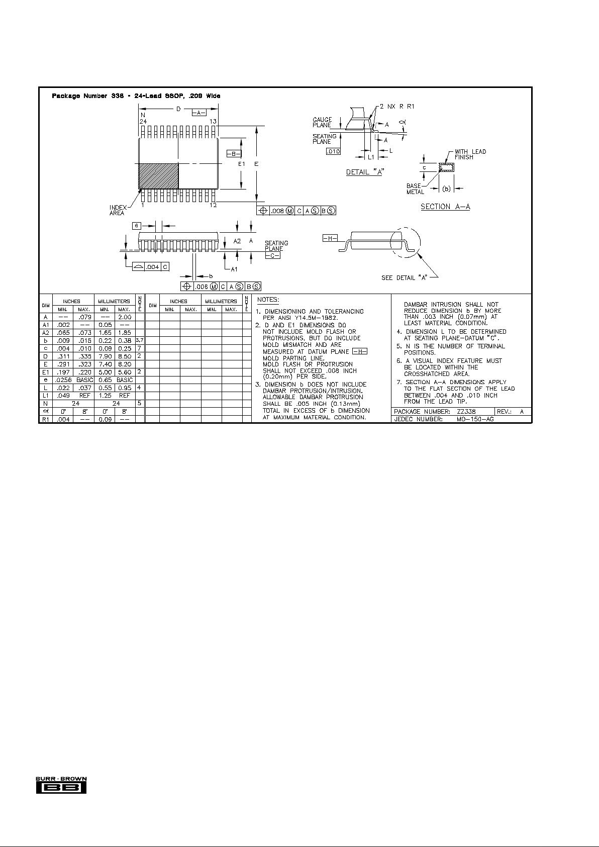
PACKAGE DRAWING
 Loading...