

Page 1
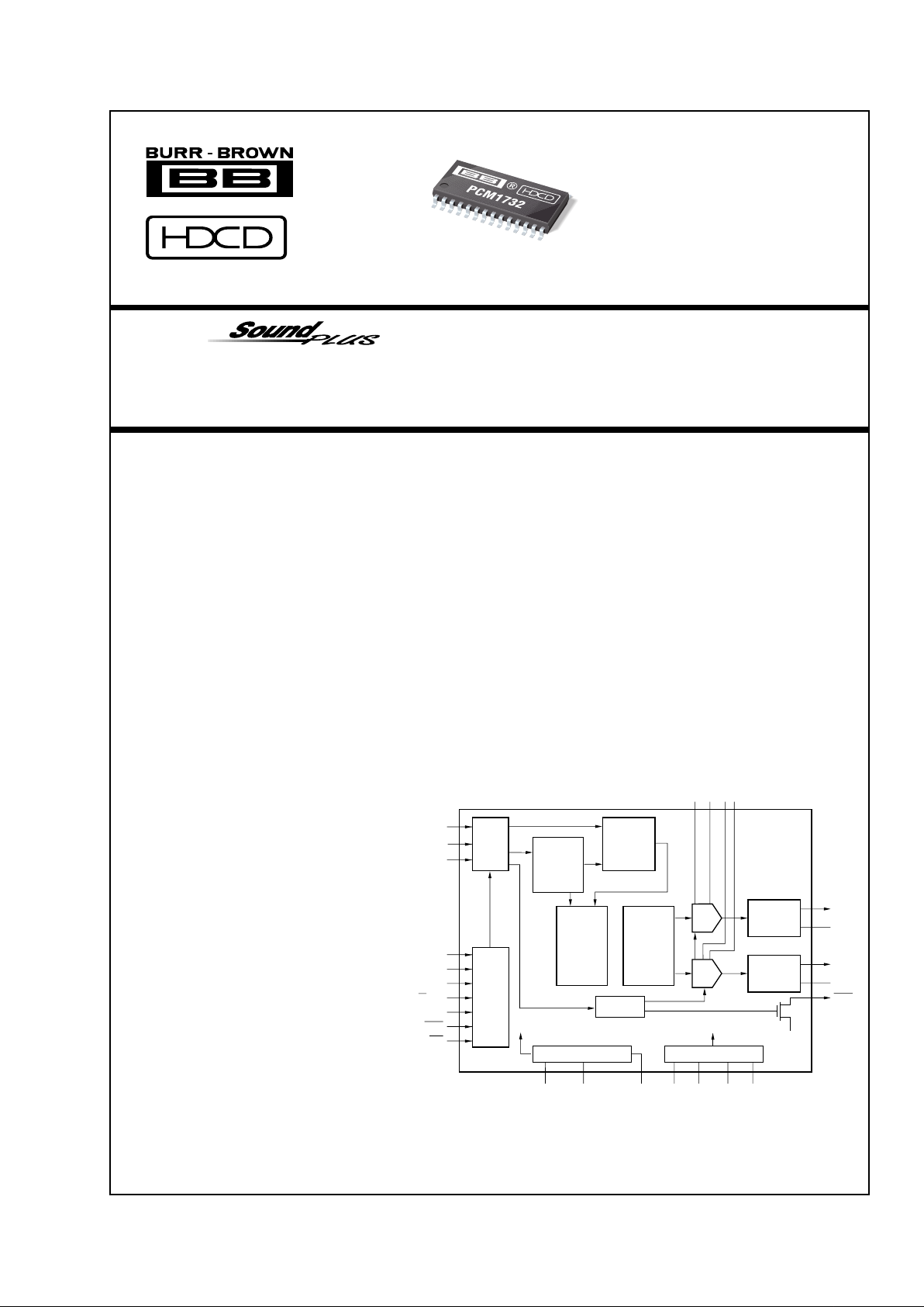
24-Bit, 96kHz, Stereo Audio
DIGITAL-TO-ANALOG CONVERTER
With HDCD® Decoder
49%
FPO
PCM1732
®
TM
FEATURES
● ENHANCED MULTI-LEVEL ∆Σ DAC
● INPUT AUDIO DATA WORD: 16-, 20-, 24-Bit
● SAMPLING FREQUENCY (fs): 16kHz - 96kHz
● SYSTEM CLOCK: 256, 384, 512, 768f
S
● HIGH PERFORMANCE:
THD+N: –96dB
Dynamic Range: 104dB
SNR: 104dB
● AUDIO OUTPUT LEVEL: 0.57 x VCC (Vp-p)
● 8x OVERSAMPLING DIGITAL FILTER WITH
HDCD DECODER:
Stopband Attenuation: –120dB
Passband Ripple: ±0.00001dB
HDCD Filter Optimized for 44.1kHz to 48kHz
and 88.2kHz to 96kHz
● MULTI-FUNCTIONS:
Digital De-emphasis
Soft Mute
Digital Attenuation
Zero Detect
Digital Gain Scaling
Reversible Output Phase
● +5V SINGLE-SUPPLY OPERATION
● SMALL SO-28 PACKAGE
© 1999 Burr-Brown Corporation PDS-1522B Printed in U.S.A. August, 1999
For most current data sheet and other product
information, visit www.burr-brown.com
®
DESCRIPTION
The PCM1732 is designed for mid- to high-grade
digital audio applications which achieve 96kHz sampling rates with 24-bit audio data, such as High Definition Compatible Digital (HDCD) CD players, DVD
players, mini-disc players and AV receivers.
PCM1732 uses a newly-developed “enhanced, multilevel delta-sigma modulator” architecture that improves audio dynamic performance and reduces jitter
sensitivity.
The internal digital filter operates at 8x oversampling
at a 96kHz sampling rate, with –120dB stopband
attenuation.
International Airport Industrial Park • Mailing Address: PO Box 11400, Tucson, AZ 85734 • Street Address: 6730 S. Tucson Blvd., Tucson, AZ 85706 • Tel: (520) 746-1111
Twx: 910-952-1111 • Internet: http://www.burr-brown.com/ • Cable: BBRCORP • Telex: 066-6491 • FAX: (520) 889-1510 • Immediate Product Info: (800) 548-6132
®
HDCD® is a registered trademark of Pacific Microsonics, Inc.
HDCD
®
technology is provided under license from Pacific Microsonics
Inc. The PCM1732’s design is covered by the following patents:
In the USA: 45,479,168, 5,638,074, 5,640,161, 5,808,574, 5,838,274
5,854,600, 5,864,311, 5,872,531.
In Australia: 669,114.
Other patents pending.
Serial
Input
I/F
Mode
Control
I/F
HDCD
Hidden
Code
Recovery
HDCD
8x
Oversampling
Digital Filter
Enhanced
Multi-Level
∆Σ
Modulator
Crystal/OSC
XTI
SCK
XTO CLKO V
CC1
AGND1 VDDDGND
HDCD
Amplitude
Decoding
V
OUT
L
V
CC2
L
V
CC2
R
AGND2R
AGND2L
EXTL
PCM1732
Open
Drain
DAC
Low-Pass
Filter
Low-Pass
Filter
BPZ Control
V
OUT
R
EXTR
ZERO
DAC
ML/I2S
MC/DEM
MD/FSS
CS/IWO
MODE
MUTE
RST
LRCIN
DIN
BCKIN
Power Supply
Power-On Reset
NOTE: An HDCD license from Pacific Microsonics, Inc. is
required to purchase the PCM1732.
Page 2
®
2
PCM1732
SPECIFICATIONS
24-Bit Data Performance
All specifications at +25°C, +VCC = +V
DD
= +5V, fS = 44.1kHz, and SYSCLK = 384fS, unless otherwise noted.
PCM1732
PARAMETER CONDITIONS MIN TYP MAX UNITS
RESOLUTION 24 Bits
DATA FORMAT
Audio Data Interface Format Standard/I
2
S
Data Bit Length 16/20/24 Selectable
Audio Data Format MSB-First, Binary Two’s Complement
Sampling Frequency (f
S
) 16 96 kHz
System Clock Frequency
(1)
256/384/512/768f
S
System Clock Duty Cycle 40 60 %
DIGITAL INPUT/OUTPUT LOGIC LEVEL
Input Logic Level (except XTI): V
IH
2.0 V
V
IL
0.8 V
Output Logic Level (CLKO): V
OH
I
OH
= 2mA 4.5 V
V
OL
I
OL
= 4mA 0.5 V
CLKO PERFORMANCE
(2)
Output Rise Time 20 ~ 80% VDD, 10pF 5.5 ns
Output Fall Time 80 ~ 20% V
DD
, 10pF 4 ns
Output Duty Cycle 10pF Load 30 %
DYNAMIC PERFORMANCE
(3, 4)
THD+N VO = 0dB fS = 44.1kHz –96 –90 dB
f
S
= 96kHz –94 dB
V
O
= –60dB fS = 44.1kHz –42 dB
Dynamic Range f
S
= 44.1kHz, EIAJ A-weighted 98 104 dB
f
S
= 96kHz, A-weighted 103 dB
Signal-to-Noise Ratio
(5)
fS = 44.1kHz, EIAJ A-weighted 98 104 dB
f
S
= 96kHz, A-weighted 103 dB
Channel Separation f
S
= 44.1kHz 96 104 dB
f
S
= 96kHz 101 dB
DC ACCURACY
Gain Error ±1.0 ±3.0 % of FSR
Gain Mismatch Channel-to-Channel ±1.0 ±3.0 % of FSR
Bipolar Zero Error V
O
= 0.5VCC at Bipolar Zero ±30 ±60 mV
ANALOG OUTPUT
Output Voltage
(6)
Full Scale (0dB) 0.57 V
CC
Vp-p
Center Voltage 0.5 V
CC
V
Load Impedance AC Load 5 kΩ
DIGITAL FILTER PERFORMANCE
Filter Characteristics 1
(f
S
= 44.1kHz/48kHz optimal)
Passband ±0.002dB 0.471f
S
–3dB 0.487f
S
Stopband 0.515f
S
Passband Ripple < 0.453f
S
±0.0001 dB
Stopband Attenuation Stopband = 0.515f
S
–109 dB
Stopband = 0.520f
S
–123 dB
Delay Time 81/f
S
sec
Filter Characteristics 2
(f
S
= 88.2kHz/96kHz optimal)
Passband ±0.005dB 0.395f
S
–3dB 0.441f
S
Stopband 0.538f
S
Passband Ripple < 0.341f
S
±0.0001 dB
Stopband Attenuation Stopband = 0.538f
S
–132 dB
Delay Time 31/f
S
sec
De-Emphasis Error ±0.1 dB
INTERNAL ANALOG FILTER
–3dB Bandwidth 100 kHz
Passband Response f = 20kHz –0.16 dB
POWER SUPPLY REQUIREMENTS
Voltage Range V
DD, VCC
4.5 5 5.5 VDC
Supply Current: I
CC
+ I
DD
fS = 44.1kHz 85 105 mA
f
S
= 96kHz 93 mA
Power Dissipation f
S
= 44.1kHz 425 525 mW
f
S
= 96kHz 465 mW
TEMPERATURE RANGE
Operating –25 +70 °C
Storage –55 +100 °C
Thermal Resistance,
θ
JA
67 °C/W
NOTES: (1) Refer to the System Clock section of this data sheet. (2) An external buffer is recommended. (3) Dynamic performance specifications are tested with 20kHz low-pass
filter and THD+N specifications are tested with 30kHz LPF, 400Hz HPF, Average Mode. (4) Dynamic performance specifications are tested with HDCD gain scaling set to analog
gain scaling. (5) SNR is tested with infinite zero detection off. (6) Output level is for sine wave. DAC outputs 0.64 V
CC
(peak-to-peak) due to filter response as transient.
Page 3
®
3 PCM1732
SPECIFICATIONS
16-Bit Data Performance
All specifications at +25°C, +VDD = +V
CC
= +5V, fS = 44.1kHz, and SYSCLK = 384fS, unless otherwise noted. For discussion of HDCD scaling options, see the
Applications Considerations section of this data sheet.
PCM1732U
PARAMETER CONDITIONS MIN TYP MAX UNITS
DYNAMIC ANALOG PERFORMANCE,
STANDARD CD, ANALOG HDCD SCALING
(1)
Total Harmonic Distortion + Noise
V
O
= 0dB 0dBFS –95 dB
V
O
= –60dB –37 dB
Dynamic Range EIAJ A-Weighted 99 dB
Output Voltage, Sine Wave 0dBFS
(2)
0.57V
CC
Vp-p
DYNAMIC ANALOG PERFORMANCE,
HDCD CD, ANALOG HDCD SCALING
(3)
Total Harmonic Distortion + Noise
VO = 0dB 0dBFS –94 dB
V
O
= –60dB –38 dB
Dynamic Range EIAJ A-Weighted
(4)
104 dB
Output Voltage, Sine Wave 0dBFS, Without Peak Extend
(2)
0.57V
CC
Vp-p
0dBFS, With Peak Extend
(5)
0.285V
CC
Vp-p
+6dBFS
(5, 6)
0.57V
CC
Vp-p
DYNAMIC ANALOG PERFORMANCE,
Standard CD, Digital HDCD SCALING
(1)
Total Harmonic Distortion + Noise
V
O
= 0dB 0dBFS –92 dB
V
O
= –60dB –33 dB
Dynamic Range EIAJ A-Weighted 96 dB
Output Voltage, Sine Wave 0dBFS 0.285V
CC
Vp-p
DYNAMIC ANALOG PERFORMANCE
HDCD CD, Digital HDCD SCALING
(2)
Total Harmonic Distortion + Noise
VO = 0dB 0dBFS –91 dB
V
O
= –60dB –34 dB
Dynamic Range EIAJ A-Weighted
(4)
104 dB
Output Voltage, Sine Wave 0dBFS 0.285V
CC
Vp-p
+6dBFS
(5)
0.57V
CC
Vp-p
NOTES: (1) Without dither. (2) Gain pin is LOW. (3) With the rectangular PDF dither. (4) Including Peak Extend to +6dBFS. (5) Gain pin is HIGH. (6) +6dBFS is
the full Peak Extend, while dynamic range numbers are with Peak Extend.
The information provided herein is believed to be reliable; however, BURR-BROWN assumes no responsibility for inaccuracies or omissions. BURR-BROWN assumes
no responsibility for the use of this information, and all use of such information shall be entirely at the user’s own risk. Prices and specifications are subject to change
without notice. No patent rights or licenses to any of the circuits described herein are implied or granted to any third party. BURR-BROWN does not authorize or warrant
any BURR-BROWN product for use in life support devices and/or systems.
Page 4
®
4
PCM1732
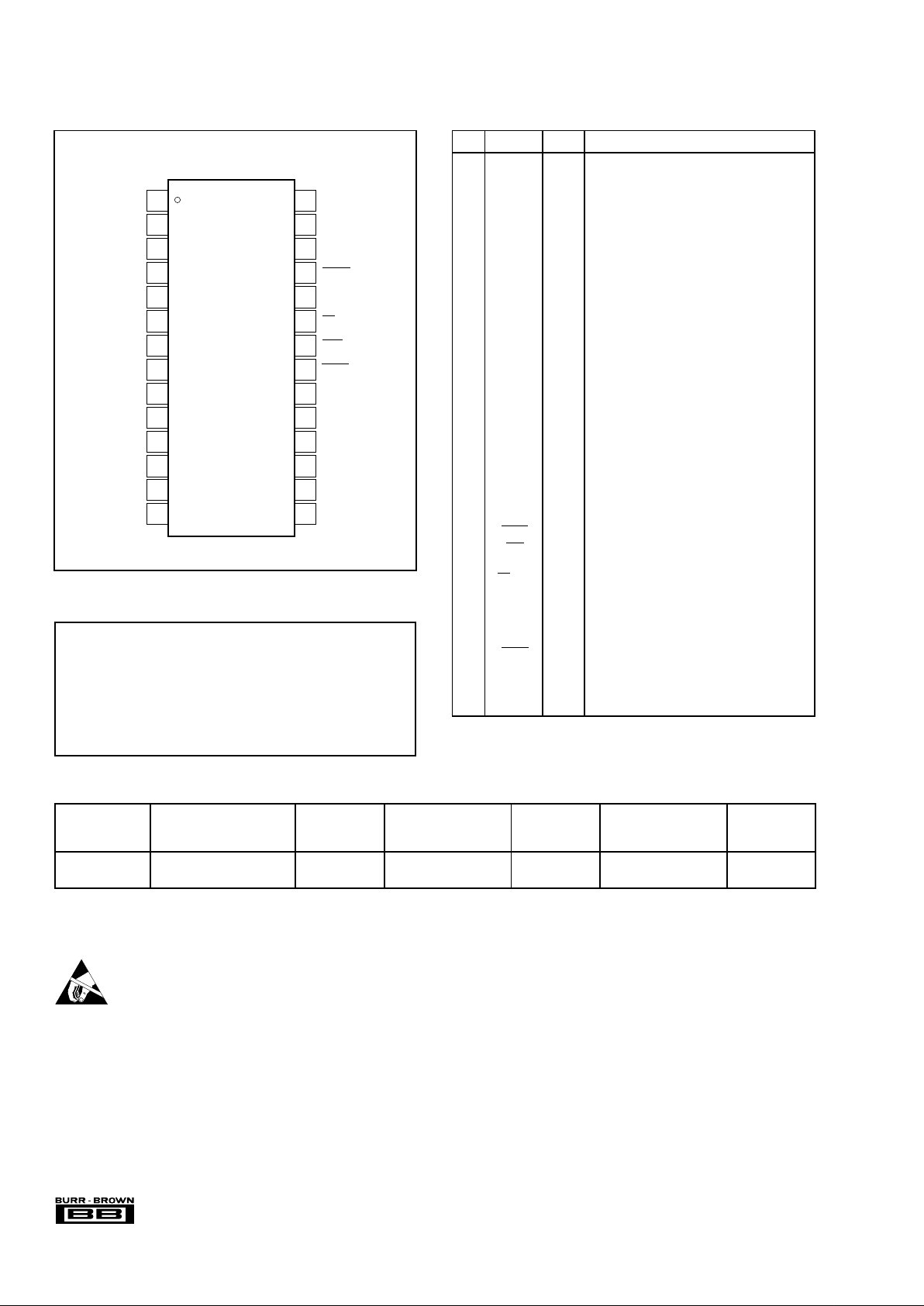
PIN NAME I/O DESCRIPTION
1 LRCIN IN Left and Right Clock Input. This clock is equal to
the sampling rate, fS.
(1)
2 DIN IN Serial Audio Data Input
(1)
3 BCKIN IN Bit Clock Input for Serial Audio Data
(1)
4 CLKO OUT Buffered System Clock Output.
5 XTI IN Oscillator Input/External Clock Input
(2)
6 XTO OUT Oscillator Output
7 DGND — Digital Ground
8V
DD
— Digital Power +5V
9 HDCD OUT HDCD Encoded Data Detect
10 V
CC
2R — Analog Power +5V, Rch
11 AGND2R — Analog Ground, Rch
12 EXTR — Common Mode Voltage for Analog Output Amp,
Rch
13 V
OUT
R OUT Analog Voltage Output, Rch
14 AGND1 — Analog Ground
15 V
CC
1 — Analog Power +5V
16 V
OUT
L OUT Analog Voltage Output, Lch
17 EXTL — Common Mode Voltage for Analog Output Amp,
Lch
18 AGND2L OUT Analog Ground, Lch
19 V
CC
2L — Analog Power +5V, Lch
20 GAIN OUT External (analog) Gain Scaling
21 ZERO OUT Zero Data Flag
22 RST IN Reset. When this pin is LOW, the digital filter
and modulators are held in reset.
(3)
23 CS/IW0 IN Chip Select/Input Format Selection. When this
pin is LOW, the Mode Control interface is enabled.
(4)
24 MODE IN
Mode Control Select: H = Software; L =
Hardware
(3)
25 MUTE IN Mute Control
(3)
26 MD/FSS IN Mode Data/Sampling Rate Range Select
(3)
27
MC/DEM
IN Mode Clock/De-Emphasis Select
(3)
28 ML/I2S IN Mode Latch/Input Format Select
(3)
NOTES: (1) Schmitt Trigger input. (2) CMOS logic level input. (3) Schmitt
Trigger input with pull-up resister. (4) Schmitt Trigger input with pull-down
resistor.
PIN ASSIGNMENTSPIN CONFIGURATION
ELECTROSTATIC
DISCHARGE SENSITIVITY
This integrated circuit can be damaged by ESD. Burr-Brown
recommends that all integrated circuits be handled with
appropriate precautions. Failure to observe proper handling
and installation procedures can cause damage.
ESD damage can range from subtle performance degradation
to complete device failure. Precision integrated circuits may
be more susceptible to damage because very small parametric
changes could cause the device not to meet its published
specifications.
Power Supply Voltage ...................................................................... +6.5V
+V
CC
to +VDD Difference ................................................................... ±0.1V
Input Logic Voltage .................................................. –0.3V to (V
DD
+ 0.3V)
Input Current (except power supply)............................................... ±10mA
Power Dissipation .......................................................................... 750mW
Operating Temperature Range ......................................... –25°C to +70°C
Storage Temperature...................................................... –55°C to +125°C
Lead Temperature (soldering, 5s)................................................. +260°C
(reflow, 10s) .................................................... +235°C
ABSOLUTE MAXIMUM RATINGS
LRCIN
DIN
BCKIN
CLKO
XTI
XTO
DGND
V
DD
HDCD
V
CC
2R
AGND2R
EXTR
V
OUT
R
AGND1
ML/I
2
S
MC/DEM
MD/FSS
MUTE
MODE
CS/IWO
RST
ZERO
GAIN
V
CC
2L
AGND2L
EXTL
V
OUT
L
V
CC
1
1
2
3
4
5
6
7
8
9
10
11
12
13
14
28
27
26
25
24
23
22
21
20
19
18
17
16
15
PCM1732U
Top View SO-28
PACKAGE SPECIFIED
DRAWING TEMPERATURE PACKAGE ORDERING TRANSPORT
PRODUCT PACKAGE NUMBER
(1)
RANGE MARKING NUMBER
(2)
MEDIA
PCM1732U SO-28 217 –25°C to +70°C PCM1732U PCM1732U Rails
"""""PCM1732U/1K Tape and Reel
NOTES: (1) For detailed drawing and dimension table, please see end of data sheet, or Appendix C of Burr-Brown IC Data Book. (2) Models with a slash (/ ) are
available only in Tape and Reel in the quantities indicated (e.g., /1K indicates 1000 devices per reel). Ordering 1000 pieces of “PCM1732U/1K” will get a single
1000-piece Tape and Reel. For detailed Tape and Reel mechanical information, refer to Appendix B of Burr-Brown IC Data Book.
PACKAGE/ORDERING INFORMATION
Page 5
®
5 PCM1732
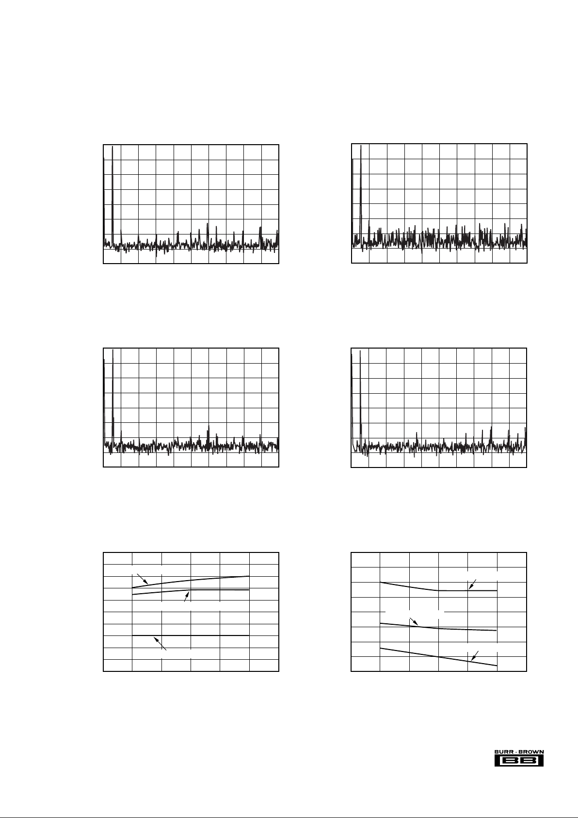
TYPICAL PERFORMANCE CURVES
All specifications at +25°C, +VCC = +V
DD
= +5V, fS = 44.1kHz, and 24-bit input data, SYSCLK = 384fS, unless otherwise noted.
108
107
106
105
104
103
102
101
100
99
98
DYNAMIC RANGE vs SUPPLY VOLTAGE
Power Supply Voltage (V)
4.25 4.50 4.75 5.00 5.25 5.50 5.75
Dynamic Range (dB)
fS = 44.1kHz, 24-Bit
fS = 44.1kHz, 16-Bit
HDCD with Peak Extend
–86
–88
–90
–92
–94
–96
98
100
–102
THD+N vs SUPPLY VOLTAGE
Power Supply Voltage (V)
4.25 4.50 4.75 5.00 5.25 5.50 5.75
THD+N at 0dB (dB)
fS = 44.1kHz, 16-Bit
HDCD With Peak Extend
fS = 44.1kHz, 24-Bit
–60
–70
–80
–90
–100
–110
–120
–130
–140
0246810
Frequency (kHz)
–60dB AMPLITUDE vs FREQUENCY
24-Bit Data
Amplitude (dB)
12 14 16 18 20
–60
–70
–80
–90
–100
–110
–120
–130
–140
–60dB AMPLITUDE vs FREQUENCY
16-Bit Data
Frequency (kHz)
0 2 4 6 8 101214161820
Amplitude (dB)
–60
–70
–80
–90
–100
–110
–120
–130
–140
–60dB AMPLITUDE vs FREQUENCY
HDCD Without Peak Extend
Frequency (kHz)
0 2 4 6 8 101214161820
Amplitude (dB)
–60
–70
–80
–90
–100
–110
–120
–130
–140
–60dB AMPLITUDE vs FREQUENCY
HDCD With Peak Extend
Frequency (kHz)
0 2 4 6 8 101214161820
Amplitude (dB)
Page 6
®
6
PCM1732
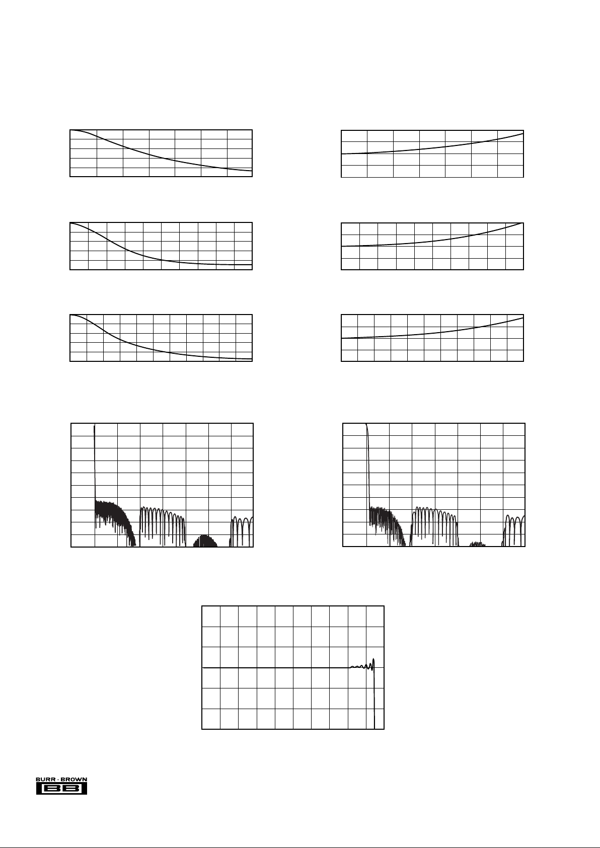
TYPICAL PERFORMANCE CURVES
DIGITAL FILTER
06
Frequency (kHz)
DE-EMPHASIS FREQUENCY RESPONSE (32kHz)
Level (dB) Level (dB)
DE-EMPHASIS FREQUENCY RESPONSE (44.1kHz)
02468101214161820
0
–2
–4
–6
–8
–10
Level (dB)
DE-EMPHASIS FREQUENCY RESPONSE (48kHz)
0 2 4 6 8 10121416182022
Frequency (kHz)
0
–2
–4
–6
–8
–10
0
2
4 6 8 10 12 14
Frequency (kHz)
0
–2
–4
–6
–8
–10
Level (dB)
0
DE-EMPHASIS ERROR (32kHz)
DE-EMPHASIS ERROR (44.1kHz)
DE-EMPHASIS ERROR (48kHz)
0 2 4 6 8 10121416182022
Frequency (kHz)
2
468101214
Frequency (kHz)
0.02
0.01
0
–0.01
–0.02
0
2
4 6 8 101214161820
Level (dB)
0.02
0.01
0
–0.01
–0.02
Level (dB)
0.04
0.02
0
–0.02
–0.04
Level (dB)
0
–20
–40
–60
–80
–100
–120
–140
–160
–180
–200
FREQUENCY RESPONSE
(De-Emphasis Off, f
S
= 44.1kHz)
Frequency (x f
S
Hz)
0 3.50.5 1.0 1.5 2.0 2.5 3.0 4.0
Amplitude (dB)
0
–20
–40
–60
–80
–100
–120
–140
–160
–180
–200
FREQUENCY RESPONSE
(FSS High, 96kHz Filter)
Frequency (x f
S
Hz)
0 3.50.5 1.0 1.5 2.0 2.5 3.0 4.0
Amplitude (dB)
0.003
0.002
0.001
0
–0.001
–0.002
–0.003
PASSBAND RIPPLE CHARACTERISTICS
Frequency (x f
S
Hz)
0 0.05 0.1 0.15 0.2 0.25 0.3 0.35 0.4 0.45 0.5
Amplitude (dB)
Page 7

®
7 PCM1732
SYSTEM CLOCK
The system clock for PCM1732 must be either 256fS, 384fS,
512fS or 768fS, where fS is the audio sampling frequency
(typically 32kHz, 44.1kHz, 48kHz, 88kHz, or 96kHz). A
768fS system clock is not supported for 88.2kHz and 96kHz
sampling frequencies.
The system clock can be either a crystal oscillator placed
between XTI (pin 5) and XTO (pin 6), or an external clock
input to XTI. If an external system clock is used, XTO is
open (floating). Figure 1 illustrates the typical system clock
connections.
PCM1732 has a system clock detection circuit which automatically senses if the system clock is operating at 256fS ~
768fS. The system clock should be synchronized with the
left/right clock (LRCIN, pin 1). LRCIN operates at the sampling frequency (fS). In the event these clocks are not
synchronized, the PCM1732 can compensate for the phase
difference internally. If the phase difference between leftright and system clocks is greater than 6-bit clocks (BCKIN),
the synchronization is performed internally. While the synchronization is processing, the analog output is forced to a
DC level at bipolar zero. The synchronization typically
occurs in less than 1 cycle of LRCIN.
SYSTEM CLOCK FREQUENCY (MHz)
SAMPLING RATE FREQUENCY (f
S
) 256f
S
384f
S
512f
S
768f
S
32kHz 8.1920 12.2880 16.3840 24.5760
44.1kHz 11.2896 16.9340 22.5792 33.8688
(1)
48kHz 12.2880 18.4320 24.5760 36.8640
(1)
88.2kHz 22.5792 33.8688
(1)
45.1584
(1)
—
96kHz 24.5760 36.8640
(1)
49.1520
(1)
—
NOTE: (1) The internal crystal oscillator frequency cannot be larger than 24.576MHz.
TABLE I. Typical System Clock Frequencies.
Typical input system clock frequencies to the PCM1732 are
shown in Table I and external input clock timing requirements are shown in Figure 2.
FIGURE 1. System Clock Connection.
FIGURE 2. XTI Clock Timing.
DATA INTERFACE FORMATS
Digital audio data is interfaced to the PCM1732 on pin 1
(LRCIN), pin 2 (DIN), and pin 3 (BCKIN). The PCM1732
can accept standard, I2S, and left-justified data formats.
Figure 3 illustrates acceptable input data formats. Figure 4
shows required timing specifications for digital audio data.
Reset
PCM1732 has both an internal power-on reset circuit and a
RST pin (pin 22), which accepts an external reset when RST
= LOW. For internal power-on reset, initialization (reset) is
done automatically at power-on when VDD > 2.2V (typical).
During internal reset = LOW, the output of the DAC is
invalid and the analog outputs are forced to VCC/ 2. Figure
5 illustrates the timing of the internal power-on reset.
PCM1732 accepts an external forced reset when RST =
LOW. When RST = LOW, the output of the DAC is invalid
and the analog outputs are forced to VCC/2 after internal
initialization (1024 system clocks count after RST = HIGH.)
Figure 6 illustrates the timing of the RST pin.
Zero Out (pin 21)
Zero is an open drain output. If the input data is continuously
zero for 65,536 cycles of BCKIN, an internal FET is switched
to “ON” and the drain of the internal FET is switched to
ground. The zero detect function is available in both software
mode and hardware mode.
System Clock
(256/384/512/768f
S
)
External Clock Input
CLKO
XTI
XTO
4
5
6
PCM1732
System Clock
Buffer Out
Crystal Resonator Oscillation
CLKO
XTI
XTO
4
5
6
PCM1732
XTAL
C
1
C
2
C1 C2 : 10pF ~ 30pF
Buffer
t
SCKH
System Clock Pulse Width HIGH: t
SCKIH
: 8ns (min)
System Clock Pulse Width LOW: t
SCKIL
: 8ns (min)
System Clock Duty: 40% to 60%
t
SCKL
70% of V
DD
30% of V
DD
H
L
XTI
Page 8

®
8
PCM1732
FIGURE 3. Audio Data Input Formats.
FIGURE 4. Audio Data Input Timing Specification.
14 15 16 1 2 3
14 15
1/f
S
L_ch
R_ch
MSB LSB
16
LRCIN (pin 1)
BCKIN (pin 3)
(1) 16-Bit Right Justified
DIN (pin 2)
1 2 3
14 15
MSB LSB
16
18 19 20 1 2 3
18 19
MSB LSB
20
(2) 20-Bit Right Justified
DIN (pin 2)
1 2 3
18 19
MSB LSB
20
23 24 1 2 3
22 23
MSB LSB
24
(3) 24-Bit Right Justified
DIN (pin 2)
(4) 24-Bit Left Justified
DIN (pin 2)
1 2 3
22 23
MSB LSB
24
1 2 3
22 23
MSB LSB
24
1 2 3
22 23
MSB LSB
24
1 2 3
14 15
1/f
S
L_ch
R_ch
MSB LSB
16
LRCIN (pin 1)
BCKIN (pin 3)
(5) 16-Bit I
2
S
DIN (pin 2)
1 2 3
14 15
MSB LSB
16
21
21
1 2 3
22 23
MSB LSB
24
(6) 24-Bit I
2
S
DIN (pin 2)
1 2 3
22 23
MSB LSB
24
LRCIN
BCKIN
DIN
1.4V
1.4V
1.4V
t
BCH
t
BCL
t
LB
t
BL
t
DS
BCKIN Pulse Cycle Time
BCKIN Pulse Width HIGH
BCKIN Pulse Width LOW
BCKIN Rising Edge to LRCIN Edge
LRCIN Edge to BCKIN Rising Edge
DIN Set-up Time
DIN Hold Time
: t
BCY
: t
BCH
: t
BCL
: t
BL
: t
LB
: t
DS
: t
DH
: 100ns (min)
: 50ns (min)
: 50ns (min)
: 30ns (min)
: 30ns (min)
: 30ns (min)
: 30ns (min)
t
DH
t
BCY
Page 9

®
9 PCM1732
FIGURE 5. Internal Power-On Reset Timing.
FUNCTIONAL DESCRIPTION
The PCM1732 can be operated in two different modes:
software or hardware mode. Software mode is a three-wire
interface using pin 28 (ML), pin 27 (MC), and pin 26 (MD).
PCM1732 can also be operated in hardware mode, where
static control signals are used on pin 28 (ML), pin 27 (DEM),
pin 26 (FSS) and pin 23 (IWO).
The mode of operation (software or hardware) is selected by
pin 24 (MODE), as shown in Table II.
TABLE II. Mode Control.
Table III indicates which functions are selectable within the
chosen mode. All of the functions shown are selectable within
the Software mode, but only de-emphasis control, soft mute
and input data format may be selected when using PCM1732
in the Hardware mode.
SOFTWARE HARDWARE
FUNCTION (Mode = H) (Mode = L)
Input Data Format Selection O P
Input Data Bit Selection O P
Input LRCIN Polarity Selection O X
Sampling Frequency Range O O
De-Emphasis Control O P
Mute O O
Attenuation O X
Infinity Zero Mute Control O X
DAC Operation Control O X
Output Phase Selection O X
CLKO Output Selection O X
NOTE: O = selectable, X = not selectable, P = partially selectable.
TABLE III. Mode Control, Selectable Functions.
FIGURE 6. External Reset Timing.
1024 system (= XTI) clocks
Reset
Reset Removal
V
CC
= V
DD
Internal Reset
XTI
1024 system (XTI) clocks
Reset
Reset Removal
XTI
Internal Reset
RST
t
RST
(1)
NOTE: (1) t
RST
= 20ns min.
CONTROL MODE (Pin 24) SELECTION
H Software
L Hardware
Page 10

®
10
PCM1732
I2S (Pin 28) IWO (Pin 23) DATA FORMAT
L L 16-Bit Data Word, Normal, Right-Justified
L H 20-Bit Data Word, Normal, Right-Justified
H L 16-Bit Data Word, I
2
S Format
H H 24-Bit Data Word, I
2
S Format
TABLE VI. Data Format Control.
SOFT MUTE
The Soft Mute function can be controlled by MUTE (pin 25).
SOFTWARE MODE (MODE = H)
The PCM1732’s special functions in the Software mode are
shown in Table VIII. These functions are controlled using a
ML, MC, MD serial control signal.
FUNCTION DEFAULT MODE
Input Audio Data Format Selection
Standard Format
Left-Justified Standard Format
I
2
S Format
Input Audio Data Bit Selection
16-Bit 16-Bit
20-Bit
24-Bit
Sampling Rate Range
f
S
≤ 52kHz fS ≤ 52kHz
f
S
> 52kHz
Input LRCIN Polarity Selection
Lch/Rch = HIGH/LOW Lch/Rch = HIGH/LOW
Lch/Rch = LOW/HIGH
De-Emphasis Control OFF
Soft Mute Control OFF
Attenuation Control
Lch, Rch Individually 0dB, Individual
Lch, Rch Common
Infinite Zero Mute Control Not Operated
DAC Operation Control Operated
Sampling Rate Selection for De-Emphasis
Standard Frequency
44.1kHz 44.1kHz
48kHz
32kHz
HDCD Hidden Code Bit Location Bit 16
Bits 16, 20, 22, 24
Output Phase Selection Not Inverted
CLKO Output Selection Input Frequency
TABLE VIII. Selectable Functions and Default.
B15 B14 B13 B12 B11 B10 B9 B8 B7 B6 B5 B4 B3 B2 B1 B0
MODE0 res res res res res A1 A0 LDL AL7 AL6 AL5 AL4 AL3 AL2 AL1 AL0
MODE1 res res res res res A1 A0 LDR AR7 AR6 AR5 AR4 AR3 AR2 AR1 AR0
MODE2 res res res res res A1 A0 CB1 CB0 SCA FSS IW1 IW0 OPE DEM MUT
MODE3 res res res res res A1 A0 IZD SF1 SF0 CK0 REV res ATC LRP I
2
S
FIGURE 7. Mode Register Mapping.
Sampling Rate Range Selection
The sampling rate range must be selected by FSS (pin 26)
as fS ≤ 52kHz or fS > 52kHz.
Input Audio Data Format
Input Data format can be selected by I2S (pin 28) and IW0
(pin 23).
B15 B14 B13 B12 B11 B10 B9 B8 B7 B6 B5 B4 B3 B2 B1 B0
ML (pin 28)
MC (pin 27)
MD (pin 26)
FIGURE 8. Three-Wire Serial Interface.
TABLE VII. Soft Mute Control.
FSS (Pin 26) SAMPLE RATE
Lf
S
≤ 52kHz
Hf
S
> 52kHz
TABLE V. Sampling Rate Range Select.
MUTE (Pin 25) SOFT MUTE
L Mute ON
H Mute OFF (normal operation)
HARDWARE MODE (MODE = L)
In Hardware mode, the following functions can be selected:
De-Emphasis Control
De-emphasis control can be selected by DEM (pin 26).
DEM (Pin 26) DE-EMPHASIS
L OFF
H Mute OFF (Normal Operation)
TABLE IV. De-Emphasis Control.
PROGRAM REGISTER BIT MAPPING
PCM1732’s special functions are controlled using four program registers which are 16 bits long. These registers are all
loaded using MD. After the 16 data bits are clocked in, ML
is used to latch in the data to the appropriate register. Figure
7 shows the complete mapping of the four registers and
Figure 8 illustrates the serial interface timing.
Page 11

®
11 PCM1732
REGISTER BIT
NAME NAME DESCRIPTION
Register 0 AL (7:0) DAC Attenuation Data for Lch
LDL Attenuation Data Load Control for Lch
A (1:0) Register Address
res Reserved, set to LOW
Register 1 AR (7:0) DAC Attenuation Data for Rch
LDR Attenuation Data Load Control for Rch
A (1:0) Register Address
res Reserved, set to LOW
Register 2 MUT Left and Right DACs Soft Mute Control
DEM De-Emphasis Control
OPE Left and Right DACs Operation Control
IW (1:0) Input Audio Data Bit and Format Select
FSS Sampling Rate Range Select
SCA HDCD Grain Scaling Select
C3 (1:0) HDCD Hidden Code Location
A (1:0) Register Address
res Reserved, set to LOW
Register 3 I
2
S Audio Data Format Select
LRP Polarity of LRCIN Select
ATC Attenuator Control
REV Output Phase Select
CKO CLKO Output Select
SF (1:0) Sampling Rate Select
IZD Internal Zero Detection Circuit Control
A (1:0) Register Address
res Reserved, set to LOW
TABLE IX. Register Functions.
REGISTER 0 (A1 = 0, A0 = 0)
B15 B14 B13 B12 B11 B10 B9 B8 B7 B6 B5 B4 B3 B2 B1 B0
res res res res res A1 A0 LDL AL7 AL6 AL5 AL4 AL3 AL2 AL1 AL0
Register 0 is used to set the attenuation data for the left
output channel.
When ATC = 1 (Bit B2 of Register MODE3 = 1), the left
channel attenuation data AL[7:0] is used for both the left and
right channel attenuators.
When ATC = 0, (Bit B2 of Register MODE3 = 0), left
channel attenuation data is taken from AL[7:0] of register
MODE0, and right channel attenuation data is taken from
AR[7:0] of register MODE1.
AL[7:0] Left Channel Attenuator Data, where AL7 is the
MSB and AL0 is the LSB.
Attenuation Level is given by:
ATTEN = 0.5 • (DATA – 255)dB
For DATA = FFH, ATTEN = –0dB
For DATA = FEH, ATTEN = –0.5dB
For DATA = 01H, ATTEN = –127.5dB
For DATA = 00H, ATTEN = infinity = Mute
FIGURE 9. Program Register Input Timing.
1.4V
1.4V
1.4V
ML
MC
MD
t
MLH
t
MCHtMCL
t
MDS
t
MCY
t
MLS
t
MLL
t
MHH
1.4V
CS
t
CSML
t
MLCS
t
MDH
LSB
MC Pulse Cycle Time
MC Pulse Width LOW
MC Pulse Width HIGH
MD Hold Time
MD Set-up Time
ML Low Level Time
ML High Level Time
ML Hold Time
ML Set-up Time
CS LOW to ML LOW Time
(2)
ML HIGH to CS HIGH Time
(2)
NOTES: (1) System Clock Cycle. (2) CS should be changed during ML = HIGH.
: t
MCY
: t
MCL
: t
MCH
: t
MDH
: t
MDS
: t
MLL
: t
MHH
: t
MLH
: t
MLS
: t
CSML
: t
MLCS
: 100ns (min)
: 40ns (min)
: 40ns (min)
: 40ns (min)
: 40ns (min)
: 40ns (min) + 1SYSCLK
(1)
(min)
: 40ns (min) + 1SYSCLK
(1)
(min)
: 40ns (min)
: 40ns (min)
: 10ns (min)
: 10ns (min)
Page 12

®
12
PCM1732
When OPE (B2) is HIGH, the output of the DAC will be
forced to bipolar zero, irrespective of any input data.
IW0(B3), IW1 (B4) and I2S (B0) of Register 3
Resisters IW0, IW1, and I2S determine the input data word
and input data format as shown in Table XIII.
IW1 IW0 I2S AUDIO INTERFACE
L L L 16-Bit Standard (Right-Justified)
L H L 20-Bit Standard (Right-Justified)
H L L 24-Bit Standard (Right-Justified)
H H L 24-Bit Left-Justified (MSB First)
L L H 16-Bit I
2
S
L H H 24-Bit I
2
S
H L H Reserved
H H H Reserved
FSS (B5) SAMPLING RATE RANGE
FSS = L Sampling Rate, f
S
≤52kHz
FSS = H Sampling Rate, f
S
>52kHz
TABLE XIII. Data Format Control.
Sampling Rate Range is selected by the FSS (B5) register.
HDCD gain scaling can be implemented internally with digital
gain scaling (for normal CD and HDCD without peak extend),
or externally with analog gain scaling (for HDCD with and
without peak extend).
Digital gain scaling is implemented by 6dB attenuation for
normal CD and HDCD without peak extend, and also operated
as 0dB attenuation for HDCD with peak extend. Detection for
normal CD, HDCD without peak extend, and HDCD with
peak extend is done automatically.
SCA (B6) GAIN SCALING
SCA = L Digital Gain Scaling
SCA = H Analog Gain Scaling
TABLE XV. Gain Scaling Select.
B15 B14 B13 B12 B11 B10 B9 B8 B7 B6 B5 B4 B3 B2 B1 B0
res res res res res A1 A0 LDR AR7 AR6 AR5 AR4 AR3 AR2 AR1 AR0
LDL Left Channel Attenuation Data Load Control.
This bit is used to simultaneously set attenuation
levels of both the Left and Right channels.
When LDL = 1, the Left channel output level is
set by the data in AL[7:0]. The Right channel
output level is set by the data in AL[7:0], or the
most recently programmed data in bits AR[7:0]
of register MODE1.
When LDL = 0, the Left channel output data
remains at its previously programmed level.
REGISTER 1 (A1 = 0, A0 = 1)
B15 B14 B13 B12 B11 B10 B9 B8 B7 B6 B5 B4 B3 B2 B1 B0
res res res res res A1 A0
CB1 CB0 SCAFSS
IW1 IWO OPE DEM MUTE
MUT (B0)
MUT = L Soft Mute OFF
MUT = H Soft Mute ON
TABLE XII. DAC Operation Control.
DEM (B1)
DEM = L De-Emphasis OFF
DEM = H De-Emphasis ON
OPE (B2)
OPE = L Normal Operation
OPE = H DAC Operation OFF
TABLE XIV. Sampling Rate Range Select.
Register 1 is used to set the attenuation data for the Right
output channel.
When ATC = 1 (Bit B2 of Register MODE3 = 1), the Left
channel attenuation data AL[7:0] of register MODE0 is used
for both the Left and Right channel attenuators.
When ATC = 0, (Bit B2 of Register MODE3 = 0), Left
channel attenuation data is taken from AL[7:0] of register
MODE0, and Right channel attenuation data is taken from
AR[7:0] of register MODE1.
AR[7:0] Right Channel Attenuator Data, where AR7 is
the MSB and AR0 is the LSB. Attenuation
Level is given by:
ATTEN = 0.5 • (DATA – 255) dB
For DATA = FFH, ATTEN = –0dB
For DATA = FEH, ATTEN = –0.5dB
For DATA = 01H, ATTEN = –127.5dB
For DATA = 00H, ATTEN = infinity = Mute
LDR Right Channel Attenuation Data Load Control.
This bit is used to simultaneously set attenuation
levels of both the Left and Right channels.
When LDR = 1, the Right channel output level
is set by the data in AR[7:0], or by the data in
bits AL[7:0] of register MODE0. The Left channel output level is set to the most recently
programmed data in bits AL[7:0] of register
MODE0.
When LDR = 0, the Right channel output data
remains at its previously programmed level.
REGISTER 2 (A1 = 1, A0 = 0)
Register 2 is used to control soft mute, de-emphasis, operation enable, input resolution, and input audio data bit and
format.
TABLE X. Soft Mute Control.
TABLE XI. De-Emphasis Control.
Page 13

®
13 PCM1732
SF1 SF0 DE-EMPHASIS SAMPLING RATE
L L Reserved
L H 48kHz
H L 44.1kHz
H H 32kHz
CKO (B5) CLOCK OUTPUT RATE
CKO = L Buffer Out of XTI Clock
CKO = H Half (1/2) Frequency Out of XTI Clock
REV (B4) DAC OUTPUT PHASE
REV = L Normal Output
REV = H Inverted Output
TABLE XVII. Zero Mute Control.
B15 B14 B13 B12 B11 B10 B9 B8 B7 B6 B5 B4 B3 B2 B1 B0
res res res res res A1 A0
IZD SF1 SF0 CKO REV
res
ATC LRP
I2S
CB1 (B8) CB0 (B7) HDCD HIDDEN CODE BIT LOCATION
L L 16th Data (default for CD)
L H 20th Data
H L Reserved
H H 24th Data
TABLE XVI. Word Length Selection for Hidden Code Bit.
IZD (B8) ZERO MUTE
IZD = L Zero Detect Mute OFF
IZD = H Zero Detect Mute ON
TABLE XVIII. De-Emphasis Sampling Rate Selection.
These bits define the location of the bit in which the PCM1732
looks for HDCD hidden code, which is inserted into the Least
Significant Bit (LSB) of the audio data.
In the case of HDCD encoded data, the HDCD hidden code
is located in the Least Significant Bit (LSB) of 16-bit audio
data. It is not necessary to change the location of this hidden
code as default.
In the case of 20-bit or 24-bit data word with HDCD
encoded input signal, this HDCD hidden code bit location
must be changed to LSB of the 20- or 24-bit word to detect
HDCD encoded signal. The word length is selected by the
CB0 and CB1 bits.
TABLE XIX. Clock Output Rate Selection.
TABLE XX. Output Phase Inversion Control.
Bits 6 (SF0) and 7 (SF1) are used to select the sampling
frequency for de-emphasis.
LRP (B1) LRCIN POLARITY
LRP = L L R H/Lch
LRP = H L R L/Lch
ATC (B2) ATTENUATION CONTROL
ATC = L Individual Channel ATT Control
ATC = H Common ATT Control
TABLE XXI. Attenuation Control Bit.
TABLE XXII. LRCIN Polarity.
REV (B4) is output analog signal phase control.
REGISTER 3 (A1 = 1, A0 = 1)
Register 3 is used to control input data format and polarity,
attenuation channel control, system clock frequency, sampling frequency, infinite zero detection, output phase,
CLKO output, and slow roll-off.
Bit 8 is used to control the Infinite Zero Detection (IZD)
function.
When IZD is LOW, the zero detect circuit is off. Under
this condition, no automatic muting will occur if the input
is continuously zero. When IZD is HIGH, the zero detect
feature is enabled. If the input data is continuously zero for
65,536 cycles of BCKIN, the output will be immediately
forced to a bipolar zero state (VCC/2). The zero detection
feature is used to avoid noise which may occur when the
input is DC. When the output is forced to bipolar zero,
there may be an audible click. PCM1732 allows the zero
detect feature to be disabled so the user can implement an
external muting circuit.
CKO (B5) is output frequency control at CLKO pin, can be
selected as buffer (1/1) or half rate of input frequency (1/2).
ATC (B2) is used as an attenuation control. When bit 3 is
set HIGH, the attenuation data on Register 0 is used for
both channels, and the data in Register 1 is ignored. When
bit 3 is LOW, each channel has separate attenuation data.
Bit 0 (I2S)is used to control the input data format. A LOW
on bit 0 sets the format to MSB-first, right-justified standard format) and a HIGH sets the format to I2S (Philips
serial data protocol). Bit 1 (LRP) is used to select the
polarity of LRCIN (left/right clock). When bit 1 is LOW,
left channel data is assumed when LRCIN is in a HIGH
phase, and right channel data is assumed when LRCIN is
in a LOW phase. When bit 1 is HIGH, the polarity
assumption is reversed. LRP applies only to standard and
left-justified data formats.
Page 14

®
14
PCM1732
FIGURE 10. 8-Level Delta-Sigma Modulator.
012345678
0
–20
–40
–60
–80
–100
–120
–140
–160
–180
Amplitude (dB)
Frequency (fS)
FIGURE 11. Quantization Noise Spectrum.
FIGURE 12. Jitter Sensitivity.
THEORY OF OPERATION
The delta-sigma DAC portion of the PCM1732 is based on
an 8-level amplitude quantizer and a 4th-order noise shaper,
which converts the oversampled input data to an 8-level
delta-sigma format.
This newly developed “enhanced multi-level delta-sigma”
architecture achieves high-grade audio dynamic performance
and sound quality.
A block diagram of the 8-level delta-sigma modulator is
shown in Figure 10. This 8-level delta-sigma modulator has
several advantages over the typical one-bit (2 level) deltasigma modulator. These advantages include improved quantization noise performance, low out-of-band noise, low idle
channel tones, and improved jitter performance.
The theoretical quantization noise performance of an 8-level
delta-sigma modulator is shown in Figure 11 and a simulated
clock jitter sensitivity plot is shown in Figure 12.
+
Z
–1
8-Level Quantizer
+
Z
–1
+
Z
–1
–
+
Z
–1
+
+
0 100 200 300 400 500 600
125
120
115
110
105
100
95
90
85
80
Dynamic Range (dB)
Input Clock Jitter (ps)
Page 15

®
15 PCM1732
In order to ensure that the average system output level of
HDCD recordings (with peak extend) match that of standard
CD and HDCD (without peak extend), analog or digital gain
scaling is implemented.
DIGITAL GAIN SCALING
Digital gain scaling is automatically performed in the digital
attenuation section by detecting HDCD material encoded
with peak extend and reducing the gain of standard CD and
HDCD encoded without peak extend by 6dB.
Digital gain scaling produces a 6dB reduciton in dynamic
range, but does not require additional analog gain scaling
circutry.
Gain scaling is controlled by the SCA bit in Register 2.
Setting SCA = 0 enables digital gain scaling. Setting SCA
= 1 enables analog gain scaling. The reset default is SCA =
0, digital gain scaling.
ANALOG GAIN SCALING
Analog gain scaling (SCA = 1) is implemented by an
external switched analog gain circuit which is controlled by
the GAIN pin (pin 20). This switched analog gain circuit
provides +6dB of gain for HDCD disks with peak extend
0dB of gain for standard CD and HDCD disks without peak
extend. Since HDCD recording with peak extend may have
peaks similiar to standard CD recordings, the analog gain
circuits must provide enough headroom for these higher
signal levels when operating with +6dB of gain.
FIGURE 13. Low-Pass Filter Response.
FIGURE 14. Low-Pass Filter Response.
HDCD GAIN REFERENCE
CD SOURCE MATERIAL PIN PIN LEVEL
Standard CD L L 0dB
HDCD Without Peak Extend H L 0dB
HDCD With Peak Extend H H –6dB
TABLE XXIII. CD Source Material and Reference Levels.
OUTPUT FILTERING
For testing purposes, all dynamic tests are performed on the
PCM1732 using a 20kHz low-pass filter. This filter limits
the measured bandwidth for THD+N, etc. to 20kHz. Failure
to use such a filter will result in higher THD+N and lower
SNR and dynamic range readings than listed in the Specifications Table. The low-pass filter removes out-of-band noise.
Although it is not audible, it may affect dynamic performance specifications.
The performance of the internal low pass filter from DC to
40kHz is shown in Figure 13. The higher frequency roll-off
of the filter is shown in Figure 14. If the user’s application
has the PCM1732 driving a wideband amplifier, it is recommended to use an external low-pass filter.
APPLICATION
CONSIDERATIONS
TYPES OF CD SOURCE MATERIAL
There are two types of HDCD recordings: HDCD encoded
data “with peak extend” and “without peak extend.” Most
HDCD recordings are encoded using peak extension which
gives them more “headroom” than standard CD and HDCD
disks without peak extend.
PCM1732 automatically detects these various types of source
materials, indicates HDCD encoded source material by the
HDCD encoded data detect (pin 9), and indicates a peak
extended source by the GAIN (pin 20). Table XXII shows
the relationship between various types of CD source material and their corresponding reference levels.
1 10 100 1k 10k 100k
1
0.5
0
–0.5
–1
Level (dB)
Frequency (Hz)
1 10 100 1k 10k 100k 1M 10M
20
0
–20
–40
–60
–80
–100
Level (dB)
Frequency (Hz)
Page 16

®
16
PCM1732
FIGURE 15. Typical Circuit Connection Diagram.
POWER SUPPLY BYPASSING
The power supplies should be bypassed as close as possible
to the device. Refer to Figure 15 for optimal values of
bypass capacitors.
POWER SUPPLY CONNECTIONS
PCM1732 has four power supply pins for digital (VDD), and
analog (VCC). Each connection also has a separate ground.
If the power supplies turn on at different times, there is a
possibility of a latch-up condition. To avoid this condition,
it is recommended to have a common connection between
the digital and analog power supplies. If separate supplies
are used without a common connection, the delta between
the two supplies during ramp-up time must be less than
0.1V.
LRCIN
DIN
BCKIN
CLKO
XTI
XTO
DGND
V
DD
HDCD
V
CC
2R
AGND2R
EXTR
V
OUT
R
AGND1
ML/I
2
S
MC/DEM
MD/FSS
MUTE
MODE
CS/IWO
RST
ZERO
GAIN
V
CC
2L
AGND2L
EXTL
V
OUT
L
V
CC
1
1
2
3
4
5
6
7
8
9
10
11
12
13
14
28
27
26
25
24
23
22
21
20
19
18
17
16
15
PCM1732U
PCM
Audio
Interface
XTAL
DGND
C
1
15pF
C
2
15pF
C
2
C
4
C
6
C
5
+V
DD
HDCD
Indicator
Post
LPF
Post
LPF
Rch Audio Out Lch Audio Out
+5V
Gain Control
(Analog Scaling)
Mode Control
C
7
10µF
C
8
10µF
C4, C5, C6 : 10µF Alum Elec or Tant || 0.1µF ceramic capacitors.
+
+
+
+
+
+
Page 17

®
17 PCM1732
FIGURE 16. Low-Pass Filter and Amplifier (relay switched).
C
305
330pF
2
3
1
8
C
303
2700pF
C
301
10µF/16V
R
301
5.6kΩ
R
305
3.9kΩ
R
309
2kΩ
R
310
2kΩ
R
303
12kΩ
1/2
OPA2134
U301
RY301
G6H-2
D301
1SS133
10 9 8 7 6
12345
+
C
307
100pF
C
309
10µF/16V
C
310
10µF/16V
6
5
7
4
R
307
2kΩ
R
311
2kΩ
1/2
OPA2134
R
308
2kΩ
U301
–
+
+
+
+
AV
CC–
(optional)
(optional)
(optional)
(optional)
(optional)
(optional)
V
CC
Q301
DTC143ESA
C
306
330pF
2
3
1
C
304
2700pF
R
306
3.9kΩ
R
302
5.6kΩ
R
304
12kΩ
1/2
OPA2134
AV
CC+
C
302
10µF/16V
+
C
308
100pF
6
5
7
R
312
2kΩ
1/2
OPA2134
U302
CN302
RCA pj
CN301
RCA pj
4
U302
C
311
10µF/16V
C
312
10µF/16V
+
+
–AV
CC
+AV
CC
V
OUT
LRY
GAIN
V
OUT
RRY
Page 18

®
18
PCM1732
FIGURE 17. Low-Pass Filter and Amplifier (transistor swtiched).
Q205
DTC144ESA
GAIN
V
OUT
R-TR
V
OUT
L-TR
Q203
DTA144ESA
Q201
2SC2878
Q204
DTA144ESA
Q202
2SC2878
C
205
330pF
2
3
1
4
U201
C
203
3900pF
CN201
RCA pj
C
201
47µF/6.3V
R
205
13kΩ
1/2
OPA2134
+
R
210
10kΩ
R
203
6.8kΩ
R
210
10kΩ
R
201
6.8kΩ
R
207
1kΩ
R
202
6.8kΩ
R
212
10kΩ
R
211
10kΩ
R
209
10kΩ
C
206
330pF
R
214
100Ω
6
5
7
8
U201
C
204
3900pF
CN202
RCA pj
C
202
47µF/6.3V
R
206
13kΩ
1/2
OPA2134
R
213
100Ω
+
R
208
1kΩ
C
207
10µF/16V
C
208
10µF/16V
A
VCC–
A
VCC+
+
+
A
VCC+
 Loading...