

Page 1

®
1
PCM1725
Stereo Audio
DIGITAL-TO-ANALOG CONVERTER
16 Bits, 96kHz Sampling
TM
PCM1725
DESCRIPTION
The PCM1725 is a complete low cost stereo audio
digital-to-analog converter (DAC), operating off of a
256fS or 384fS system clock. The DAC contains a 3rdorder ∆Σ modulator, a digital interpolation filter, and
an analog output amplifier. The PCM1725 accepts
16-bit input data in either normal or I
2
S formats.
The digital filter performs an 8X interpolation function
and includes de-emphasis at 44.1kHz. The PCM1725
can accept digital audio sampling frequencies from
16kHz to 96kHz, always at 8X oversampling.
The PCM1725 is ideal for low-cost, CD-quality consumer audio applications.
®
FEATURES
● COMPLETE STEREO DAC: Includes Digital
Filter and Output Amp
● DYNAMIC RANGE: 95dB
● MULTIPLE SAMPLING FREQUENCIES:
16kHz to 96kHz
● 8X OVERSAMPLING DIGITAL FILTER
● SYSTEM CLOCK: 256f
S
/ 384f
S
● NORMAL OR I2S DATA INPUT FORMATS
● SMALL 14-PIN SOIC PACKAGE
PCM1725
International Airport Industrial Park • Mailing Address: PO Box 11400, Tucson, AZ 85734 • Street Address: 6730 S. Tucson Blvd., Tucson, AZ 85706 • Tel: (520) 746-1111 • Twx: 910-952-1111
Internet: http://www.burr-brown.com/ • FAXLine: (800) 548-6133 (US/Canada Only) • Cable: BBRCORP • Telex: 066-6491 • FAX: (520) 889-1510 • Immediate Product Info: (800) 548-6132
Serial
Input
I/F
Mode
Control
I/F
8X Oversampling
Digital Filter
SCKI
256f
S
/384f
S
V
CC
GND
Multi-level
Delta-Sigma
Modulator
V
OUT
L
CAP
DAC
Multi-level
Delta-Sigma
Modulator
Low-pass
Filter
Low-pass
Filter
V
OUT
R
DAC
FORMAT
LRCIN
DIN
BCKIN
DM
Power Supply
© 1997 Burr-Brown Corporation PDS-1373C Printed in U.S.A. January, 1998
Page 2
®
2
PCM1725
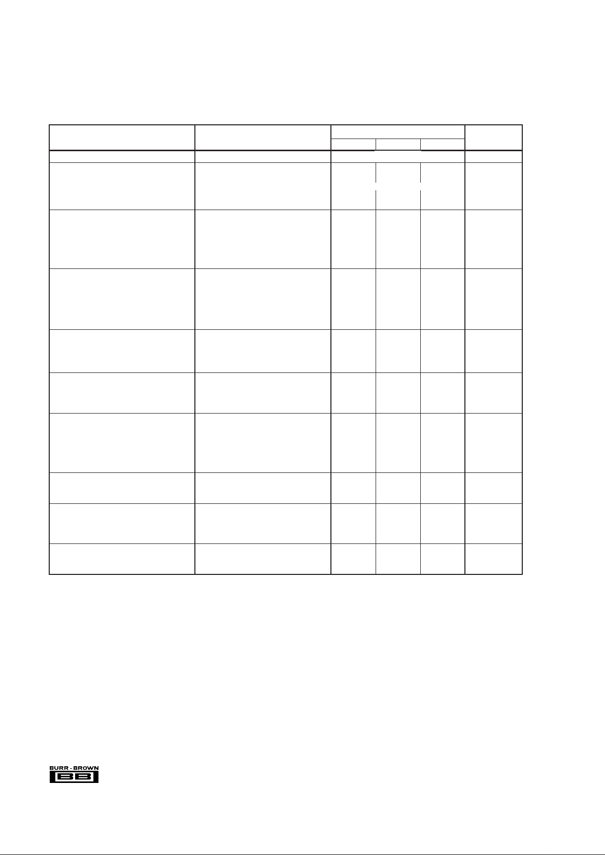
SPECIFICATIONS
All specifications at +25°C, +V
CC
= +5V, fS = 44.1kHz, and 16-bit input data, SYSCLK = 384fS, unless otherwise noted.
The information provided herein is believed to be reliable; however, BURR-BROWN assumes no responsibility for inaccuracies or omissions. BURR-BROWN assumes
no responsibility for the use of this information, and all use of such information shall be entirely at the user’s own risk. Prices and specifications are subject to change
without notice. No patent rights or licenses to any of the circuits described herein are implied or granted to any third party. BURR-BROWN does not authorize or warrant
any BURR-BROWN product for use in life support devices and/or systems.
PCM1725
PARAMETER CONDITIONS MIN TYP MAX UNITS
RESOLUTION 16 Bits
DATA FORMAT
Audio Data Interface Format Standard / I
2
S
Audio Data Format Binary Two’s Complement
Sampling Frequency (f
S
) 16 96 kHz
Internal System Clock Frequency 256f
S
/384f
S
DIGITAL INPUT/OUTPUT
Logic Level TTL
Input Logic Level
V
IH
(1)
2.0 VDC
V
IL
(1)
0.8 VDC
Input Logic Current: I
IN
(1)
±0.8 µA
DYNAMIC PERFORMANCE
(2)
f = 991kHz
THD+N at FS (0dB) –83 –78 dB
THD+N at –60dB –32 dB
Dynamic Range A-weighted 90 95 dB
Signal-to-Noise Ratio A-weighted 90 97 dB
Channel Separation 88 95 dB
DC ACCURACY
Gain Error ±1.0 ±5.0 % of FSR
Gain Mismatch, Channel-to-Channel ±1.0 ±5.0 % of FSR
Bipolar Zero Error V
OUT
= VCC/2 at BPZ ±20 ±50 mV
ANALOG OUTPUT
Output Voltage Full Scale (0dB) 0.62 x V
CC
Vp-p
Center Voltage V
CC
/2 VDC
Load Impedance AC Load 10 kΩ
DIGITAL FILTER PERFORMANCE
Passband 0.445 f
S
Stopband 0.555 f
S
Passband Ripple ±0.17 dB
Stopband Attenuation –35 dB
Delay Time 11.125/f
S
sec
INTERNAL ANALOG FILTER
–3dB Bandwidth 100 kHz
Passband Response f = 20kHz –0.16 dB
POWER SUPPLY REQUIREMENTS
Voltage Range 4.5 5 5.5 VDC
Supply Current 13 18 mA
Power Dissipation 65 90 mW
TEMPERATURE RANGE
Operation –25 +85 °C
Storage –55 +125 °C
NOTES: (1) Pins 1, 2, 3, 12, 13: LRCIN, DIN, BCKIN, DM, FORMAT (Schmitt Trigger Input); Pin 14: SCKI. (2) Dynamic performance specs are tested with 20kHz
low pass filter and THD+N specs are tested with 30kHz LPF, 400Hz HPF, Average-Mode.
Page 3
®
3
PCM1725
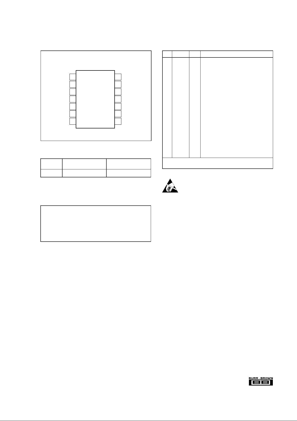
PIN ASSIGNMENTS
PIN NAME I/O FUNCTION
1
(1)
LRCIN IN Sample Rate Clock Input
2
(1)
DIN IN Audio Data Input
3
(1)
BCKIN IN Bit Clock Input for Audio Data.
4 NC — No Connection
5 CAP — Common Pin of Analog Output Amp
6V
OUT
R OUT Right-Channel Analog Output
7 GND — Ground
8V
CC
— Power Supply
9V
OUT
L OUT Left-Channel Analog Output
10 NC — No Connection
11 NC — No Connection
12
(2)
DM IN De-emphasis Control
HIGH: De-emphasis ON
LOW: De-emphasis OFF
13
(2)
FORMAT — Audio Data Format Select
HIGH: I
2
S Data Format
LOW: Standard Data Format
14 SCKI IN System Clock Input (256f
S
or 384fS)
NOTES: (1) Schmitt Trigger input. (2) Schmitt Trigger input with internal
pull-up.
PIN CONFIGURATION
TOP VIEW SOIC
LRCIN
DIN
BCKIN
NC
CAP
V
OUT
R
GND
SCKI
FORMAT
DM
NC
NC
V
OUT
L
V
CC
1
2
3
4
5
6
7
14
13
12
11
10
9
8
PCM1725
PACKAGE INFORMATION
PACKAGE DRAWING
PRODUCT PACKAGE NUMBER
(1)
PCM1725U 14 Pin SOIC 235
NOTE: (1) For detailed drawing and dimension table, please see end of data
sheet, or Appendix C of Burr-Brown IC Data Book.
ABSOLUTE MAXIMUM RATINGS
Power Supply Voltage.......................................................................+6.5V
+V
CC
to +VDD Difference ...................................................................±0.1V
Input Logic Voltage ..................................................–0.3V to (V
DD
+ 0.3V)
Power Dissipation ..........................................................................290mW
Operating Temperature Range .........................................–25°C to +85°C
Storage Temperature...................................................... –55°C to +125°C
Lead Temperature (soldering, 5s).................................................. +260°C
Thermal Resistance,
θ
JA
..............................................................+90°C/W
ELECTROSTATIC
DISCHARGE SENSITIVITY
This integrated circuit can be damaged by ESD. Burr-Brown
recommends that all integrated circuits be handled with
appropriate precautions. Failure to observe proper handling
and installation procedures can cause damage.
ESD damage can range from subtle performance degradation
to complete device failure. Precision integrated circuits may
be more susceptible to damage because very small parametric
changes could cause the device not to meet its published
specifications.
Page 4

®
4
PCM1725
TYPICAL PERFORMANCE CURVES
At TA = +25°C, +VCC = +5V, fS = 44.1kHz, SYSCLK = 256fS, unless otherwise noted.
DYNAMIC PERFORMANCE
THD+N vs TEMPERATURE
Temperature (°C)
THD+N at 0dB (%)
0.009
0.008
0.007
0.006
0.005
0.004
0.003
0.002
0.001
0
–25 0 25 50 75 85 100
THD+N at –60dB (%)
3.2
3.1
3.0
2.9
2.8
2.7
2.6
2.5
2.4
2.3
–60dB
0dB
SNR, DYNAMIC RANGE vs TEMPERATURE
Temperature (°C)
SNR (dB)
99
98
97
96
95
94
93
99
98
97
96
95
94
93
–25 0 25 50 75 85 100
Dynamic Range (dB)
Dynamic Range
SNR
THD+N vs POWER SUPPLY
V
CC
(V)
THD+N at 0dB (%)
0.009
0.008
0.007
0.006
0.005
0.004
0.003
0.002
0.001
0
4.5 4.75 5.0 5.25 5.5
THD+N at –60dB (%)
3.2
3.1
3.0
2.9
2.8
2.7
2.6
2.5
2.4
2.3
–60dB
0dB
THD+N vs SAMPLING RATE
Sampling Rate (kHz)
THD+N at 0dB (%)
0.016
0.014
0.012
0.01
0.008
0.006
0.004
5.2
4.7
4.2
3.7
3.2
2.7
2.2
44.1 48 88.2 96
THD+N AT –60dB (%)
–60dB
0dB
SNR, DYNAMIC RANGE vs SAMPLING RATE
Sampling Rate (kHz)
SNR (dB)
98
97
96
95
94
93
92
91
90
89
88
98
97
96
95
94
93
92
91
90
89
88
44.1 48 88.2 96
Dynamic Range (dB)
Dynamic Range
SNR
SNR, DYNAMIC RANGE vs POWER SUPPLY
V
CC
(V)
SNR (dB)
99
98
97
96
95
94
93
99
98
97
96
95
94
93
4.5 4.75 5.0 5.25 5.5
Dynamic Range (dB)
Dynamic Range
SNR
Page 5

®
5
PCM1725
TYPICAL PERFORMANCE CURVES
At TA = +25°C, +VCC = +V
DD
= +5V, fS = 44.1kHz, and 16-bit input data, SYSCLK = 384fS, unless otherwise noted.
DIGITAL FILTER
0 0.4536fS1.3605fS2.2675fS3.1745fS4.0815f
S
0
–20
–40
–60
–80
–100
dB
OVERALL FREQUENCY CHARACTERISTIC
Frequency (Hz)
PASSBAND RIPPLE CHARACTERISTIC
0
–0.2
–0.4
–0.6
–0.8
–1
0 0.1134f
S
0.2268f
S
0.3402f
S
0.4535f
S
dB
Frequency (Hz)
DE-EMPHASIS FREQUENCY RESPONSE (44.1kHz)
Frequency (kHz)
Level (dB)
0
–2
–4
–6
–8
–10
–12
0 5 10 15 20 25
DE-EMPHASIS FREQUENCY ERROR (44.1kHz)
Frequency (kHz)
Error (dB)
0.6
0.4
0.2
0.0
–0.2
–0.4
–0.6
0 4999.8375 9999.675 14999.5125 19999.35
Page 6

®
6
PCM1725
FIGURE 1. “Normal” Data Input Timing.
FIGURE 2. “I2S” Data Input Timing.
LRCKIN
BCKIN
DIN
1.4V
1.4V
1.4V
t
BCH
t
BCL
t
LB
t
BL
t
DS
BCKIN Pulse Cycle Time
BCKIN Pulse Width High
BCKIN Pulse Width Low
BCKIN Rising Edge to LRCIN Edge
LRCIN Edge to BCKIN Rising Edge
DIN Set-up Time
DIN Hold Time
: t
BCY
: t
BCH
: t
BCL
: t
BL
: t
LB
: t
DS
: t
DH
: 100ns (min)
: 50ns (min)
: 50ns (min)
: 30ns (min)
: 30ns (min)
: 30ns (min)
: 30ns (min)
t
DH
t
BCY
FIGURE 3. Audio Data Input Timing.
SYSTEM CLOCK
The system clock for PCM1725 must be either 256f
S
or
384f
S
, where fS is the audio sampling frequency (LRCIN),
typically 32kHz, 44.1kHz or 48kHz. The system clock is
used to operate the digital filter and the noise shaper. The
system clock input (SCKI) is at pin 14. Timing conditions
for SCKI are shown in Figure 4.
System Clock Pulse Width High t
SCKIH
13ns (min)
System Clock Pulse Width Low t
SCKIL
13ns (min)
t
SCKIH
SCKI
t
SCKIL
2.0V
0.8V
FIGURE 4. System Clock Timing Requirements.
14 15 16 1 2 3
14 15
1/fs
L_ch
R_ch
MSB LSB
16
LRCIN (pin 1)
BCKIN (pin 3)
AUDIO DATA WORD = 16-BIT
DIN (pin 2)
1 2 3
14 15
MSB LSB
16
1 2 3
14 15
1/fs
L_ch
R_ch
MSB LSB
16
LRCIN (pin 1)
BCKIN (pin 3)
AUDIO DATA WORD = 16-BIT
DIN (pin 2)
1 2 3
14 15
MSB LSB
16
21
Page 7

®
7
PCM1725
PCM1725 has a system clock detection circuit which automatically detects the frequency, either 256f
S
or 384fS. The
system clock should be synchronized with LRCIN (pin 1),
but PCM1725 can compensate for phase differences. If the
phase difference between LRCIN and system clock is greater
than ±6 bit clocks (BCKIN), the synchronization is performed automatically. The analog outputs are forced to a
bipolar zero state (VCC/2) during the synchronization function. Table I shows the typical system clock frequency
inputs for the PCM1725.
SYSTEM CLOCK
FREQUENCY (MHz)
256f
S
384f
S
32kHz 8.192 12.288
44.1kHz 11.2896 16.9340
48kHz 12.288 18.432
SAMPLING
RATE (LRCIN)
TABLE I. System Clock Frequencies vs Sampling Rate.
TYPICAL CONNECTION DIAGRAM
Figure 5 illustrates the typical connection diagram for
PCM1725 used in a stand-alone application.
INPUT DATA FORMAT
PCM1725 can accept input data in either normal (MSB-first,
right-justified) or I
2
S formats. When pin 13 (FORMAT) is
LOW, normal data format is selected; a HIGH on pin 13
selects I2S format.
FORMAT
0 Normal Format (MSB-first, right-justified)
1I
2
S Format (Philips serial data protocol)
TABLE II. Input Format Selection.
FIGURE 6. Internal Power-On Reset Timing.
DIN
BCKIN
LRCIN
2
3
1
13
12
FORMAT
DM
SCKI
9
5
78
6
14
PCM
Audio Data
Processor
256f
S
/384fS CLK
GND
Mode Control
Lch Analog Out
+5V Analog
Rch Analog Out
V
CC
V
OUT
L
V
OUT
R
CAP
PCM1725
+
10µF
Post
LPF
Post
LPF
FIGURE 5. Typical Connection Diagram.
RESET
PCM1725 has an internal power-on reset circuit. The internal
power-on reset initializes (resets) when the supply voltage
VCC > 2.2V (typ). The power-on reset has an initialization
period equal to 1024 system clock periods after V
CC
> 2.2V.
During the initialization period, the outputs of the DAC are
invalid, and the analog outputs are forced to VCC/2. Figure 6
illustrates the power-on reset and reset-pin reset timing.
DE-EMPHASIS CONTROL
Pin 12 (DM) enables PCM1725’s de-emphasis function. Deemphasis operates only at 44.1kHz.
DM
0 DEM OFF
1 DEM ON (44.1kHz)
TABLE III. De-Emphasis Control Selection.
1024 system (= SCKI) clocks
Reset
Reset Removal
2.6V
2.2V
1.8V
V
CC
Internal Reset
SCKI Clock
Page 8

®
8
PCM1725
APPLICATION
CONSIDERATIONS
DELAY TIME
There is a finite delay time in delta-sigma converters. In A/D
converters, this is commonly referred to as latency. For a
delta-sigma D/A converter, delay time is determined by the
order number of the FIR filter stage, and the chosen sampling
rate. The following equation expresses the delay time of
PCM1725:
T
D
= 11.125 x 1/f
S
For fS = 44.1kHz, TD = 11.125/44.1kHz = 251.4µs
Applications using data from a disc or tape source, such as
CD audio, CD-Interactive, Video CD, DAT, Minidisc,
etc., generally are not affected by delay time. For some
professional applications such as broadcast audio for studios, it is important for total delay time to be less than 2ms.
OUTPUT FILTERING
For testing purposes all dynamic tests are done on the
PCM1725 using a 20kHz low pass filter. This filter limits
the measured bandwidth for THD+N, etc. to 20kHz. Failure
to use such a filter will result in higher THD+N and lower
SNR and Dynamic Range readings than are found in the
specifications. The low pass filter removes out of band
noise. Although it is not audible, it may affect dynamic
specification numbers.
The performance of the internal low pass filter from DC to
24kHz is shown in Figure 7. The higher frequency rolloff of
the filter is shown in Figure 8. If the user’s application has
the PCM1725 driving a wideband amplifier, it is recommended to use an external low pass filter. A simple 3rdorder filter is shown in Figure 9. For some applications, a
passive RC filter or 2nd-order filter may be adequate.
BYPASSING POWER SUPPLIES
The power supplies should be bypassed as close as possible
to the unit. It is also recommended to include a 0.1µF ceramic
capacitor in parallel with the 10µF tantalum bypass capacitor.
1.0
0.5
0
–0.5
–1.0
dB
20
Frequency (Hz)
100 1k 10k 24k
INTERNAL ANALOG FILTER FREQUENCY RESPONSE
(20Hz~24kHz, Expanded Scale)
FIGURE 7. Low Pass Filter Frequency Response.
10
5
0
–5
–10
–15
–20
–25
–30
–35
–40
–45
–50
–55
10 100 1k 10k 100k 1M 10M
Frequency (Hz)
dB
–60
INTERNAL ANALOG FILTER FREQUENCY RESPONSE
(10Hz~10MHz)
FIGURE 8. Low Pass Filter Wideband Frequency Response.
10kΩ
10kΩ
10kΩ
1500pF
100pF
680pF
+
V
SIN
–
90
0
–90
–180
–270
–360
100 1k 10k 100k 1M
GAIN vs FREQUENCY
Frequency (Hz)
Phase (°)
6
–14
–34
–54
–74
–94
Gain (dB)
Gain
Phase
OPA134
FIGURE 9. 3rd-Order LPF.
Page 9

®
9
PCM1725
FIGURE 10. 5-Level ∆Σ Modulator Block Diagram.
FIGURE 11. Quantization Noise Spectrum.
Out
48f
S
(384fS)
64f
S
(256fS)
In
8f
S
18-Bit
+
++
4
3
2
1
0
5-level Quantizer
+
–
+
Z
–1
+
–
+
Z
–1
+
+
Z
–1
THEORY OF OPERATION
The delta-sigma section of PCM1725 is based on a 5-level
amplitude quantizer and a 3rd-order noise shaper. This
section converts the oversampled input data to 5-level deltasigma format. A block diagram of the 5-level delta-sigma
modulator is shown in Figure 10. This 5-level delta-sigma
modulator has the advantage of stability and clock jitter over
the typical one-bit (2-level) delta-sigma modulator.
The combined oversampling rate of the delta-sigma modulator and the internal 8X interpolation filter is 96f
S
for a
384f
S
system clock, and 64fS for a 256fS system clock. The
theoretical quantization noise performance of the 5-level
delta-sigma modulator is shown in Figure 11.
5-LEVEL ∆Σ MODULATOR
Frequency (kHz)
Gain (–dB)
20
0
–20
–40
–60
–80
–100
–120
–140
–160
0 5 10 15 20 25
 Loading...