

Page 1
© 1996 Burr-Brown Corporation PDS-1333B Printed in U.S.A. August, 1996
Serial
Input
I/F
Mode
Control
I/F
8X Oversampling
Digital Filter
with Function
Controller
SCKI
256f
S
/384f
S
VCCAGND
Multi-level
Delta-Sigma
Modulator
V
OUT
L
CAP
Open Drain
DAC
Multi-level
Delta-Sigma
Modulator
Low-pass
Filter
Low-pass
Filter
BPZ-Cont.
V
OUT
R
ZERO
DAC
MC
MD
ML
LRCIN
DIN
BCKIN
RSTB
Power Supply
VDDDGND
Stereo Audio
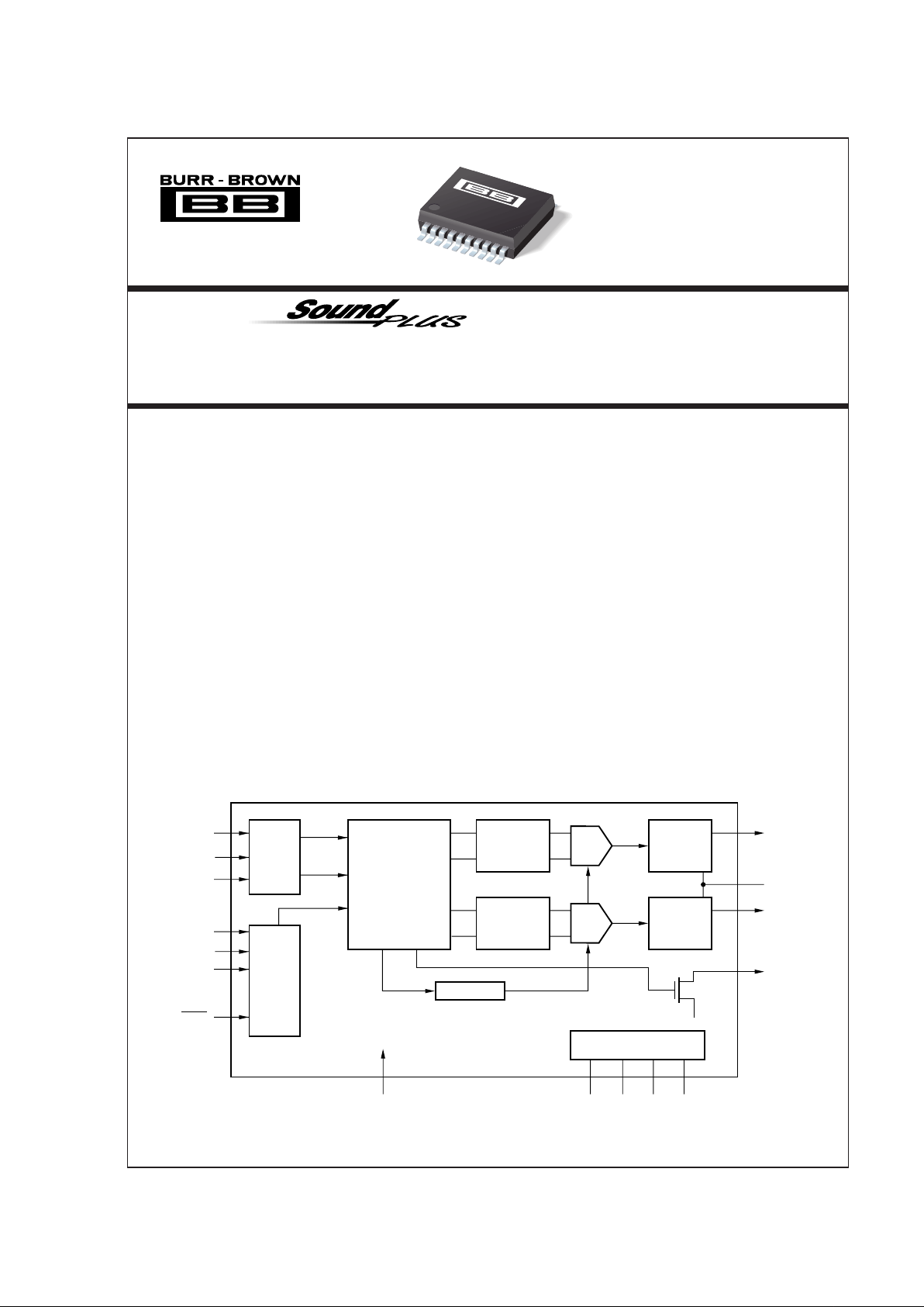
DIGITAL-TO-ANALOG CONVERTER
MPEG2/AC-3 COMPATIBLE
TM
49%
FPO
PCM1720
DESCRIPTION
The PCM1720 is a complete low cost stereo audio
digital-to-analog converter (DAC), operating off of a
256fS or 384fS system clock. The DAC contains a 3rdorder ∆Σ modulator, a digital interpolation filter, and
an analog output amplifier. The PCM1720 can accept
16-, 20-, or 24-bit input data in either normal or I
2
S
formats.
The digital filter performs an 8X interpolation func-
tion and includes selectable features such as soft mute,
digital attenuation and digital de-emphasis. The
PCM1720 can accept standard digital audio sampling
frequencies as well as one-half and double sampling
frequencies.
The PCM1720 is ideal for applications which combine
compressed audio and video data such as DVD, DVDROM, set-top boxes and MPEG sound cards.
®
FEATURES
● ACCEPTS 16-, 20-, OR 24-BIT INPUT DATA
● COMPLETE STEREO DAC: Includes Digital
Filter and Output Amp
● DYNAMIC RANGE: 96dB
● MULTIPLE SAMPLING FREQUENCIES:
16kHz to 96kHz
8X Oversampling at All Sampling
Frequencies
● SYSTEM CLOCK: 256f
S
/384f
S
● NORMAL OR I2S DATA INPUT FORMATS
● SELECTABLE FUNCTIONS:
Soft Mute
Digital Attenuator (256 Steps)
Digital De-emphasis
● OUTPUT MODE: Left, Right, Mono, Mute
International Airport Industrial Park • Mailing Address: PO Box 11400, Tucson, AZ 85734 • Street Address: 6730 S. Tucson Blvd., Tucson, AZ 85706 • Tel: (520) 746-1111 • Twx: 910-952-1111
Internet: http://www.burr-brown.com/ • FAXLine: (800) 548-6133 (US/Canada Only) • Cable: BBRCORP • Telex: 066-6491 • FAX: (520) 889-1510 • Immediate Product Info: (800) 548-6132
®
PCM1720
Page 2
®
PCM1720
2
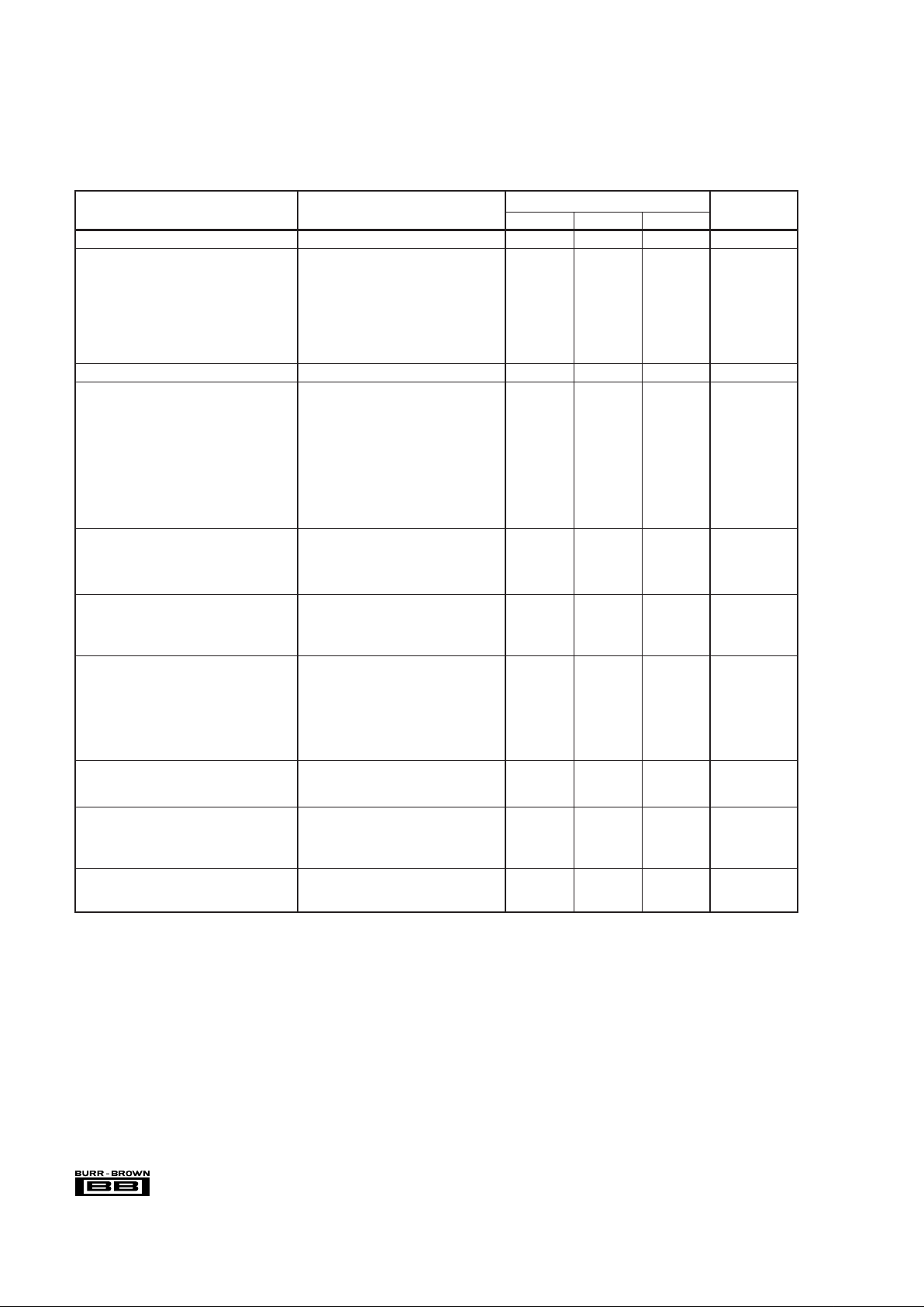
SPECIFICATIONS
All specifications at +25°C, +VCC = +V
DD
= +5V, fS = 44.1kHz, and 16-bit input data, SYSCLK = 384fS, unless otherwise noted.
PCM1720
PARAMETER CONDITIONS MIN TYP MAX UNITS
RESOLUTION 16 24 Bits
DATA FORMAT
Audio Data Format Standard/I
2
S
Data Bit Length 16/20/24
Selectable
Sampling Frequency (f
S
) Standard f
S
32 44.1 48 kHz
One-half f
S
16 22.05 24 kHz
Double f
S
64 88.2 96 kHz
Internal System Clock Frequency 256f
S
/384f
S
DIGITAL INPUT/OUTPUT LOGIC LEVEL TTL
DYNAMIC PERFORMANCE
(1)
THD+N at fS (0dB) fS = 44.1kHz –90 –80 dB
f
S
= 96kHz –88 dB
THD+N at –60dB f
S
= 44.1kHz –34 dB
f
S
= 96kHz –31 dB
Dynamic Range f
S
= 44.1kHz 90 96 dB
f
S
= 96kHz 93 dB
Signal-to-Noise Ratio
(2)
fS = 44.1kHz 92 100 dB
f
S
= 96kHz 97 dB
Channel Separation f
S
= 44.1kHz 90 97 dB
DC ACCURACY
Gain Error ±1.0 ±5.0 % of FSR
Gain Mismatch, Channel-to-Channel ±1.0 ±5.0 % of FSR
Bipolar Zero Error V
OUT
= VCC/2 at BPZ ±30 mV
ANALOG OUTPUT
Output Voltage Full Scale (0dB) 0.62 x V
CC
Vp-p
Center Voltage V
CC
/2 VDC
Load Impedance AC Load 5 kΩ
DIGITAL FILTER PERFORMANCE
Passband 0.445 f
S
Stopband 0.555 f
S
Passband Ripple ±0.17 dB
Stopband Attenuation –35 dB
Delay Time 11.125/f
S
sec
De-emphasis Error –0.2 +0.55 dB
INTERNAL ANALOG FILTER
–3dB Bandwidth 100 kHz
Passband Response f = 20kHz –0.16 dB
POWER SUPPLY REQUIREMENTS
Voltage Range V
DD
, V
CC
4.5 5 5.5 VDC
Supply Current: I
CC + IDD
VCC = VDD = 5V, fS = 44.1kHz 18 25 mA
V
CC
= VDD = 5V, fS = 96kHz 25 35 mA
TEMPERATURE RANGE
Operation –25 +85 °C
Storage –55 +100 °C
NOTES: (1) Dynamic performance specs are tested with 20kHz low pass filter and THD+N specs are tested with 30kHz LPF, 400Hz HPF, Average-Mode. (2) SNR
is tested with Infinite Zero Detection off.
The information provided herein is believed to be reliable; however, BURR-BROWN assumes no responsibility for inaccuracies or omissions. BURR-BROWN assumes
no responsibility for the use of this information, and all use of such information shall be entirely at the user’s own risk. Prices and specifications are subject to change
without notice. No patent rights or licenses to any of the circuits described herein are implied or granted to any third party. BURR-BROWN does not authorize or warrant
any BURR-BROWN product for use in life support devices and/or systems.
Page 3
®
PCM1720
3
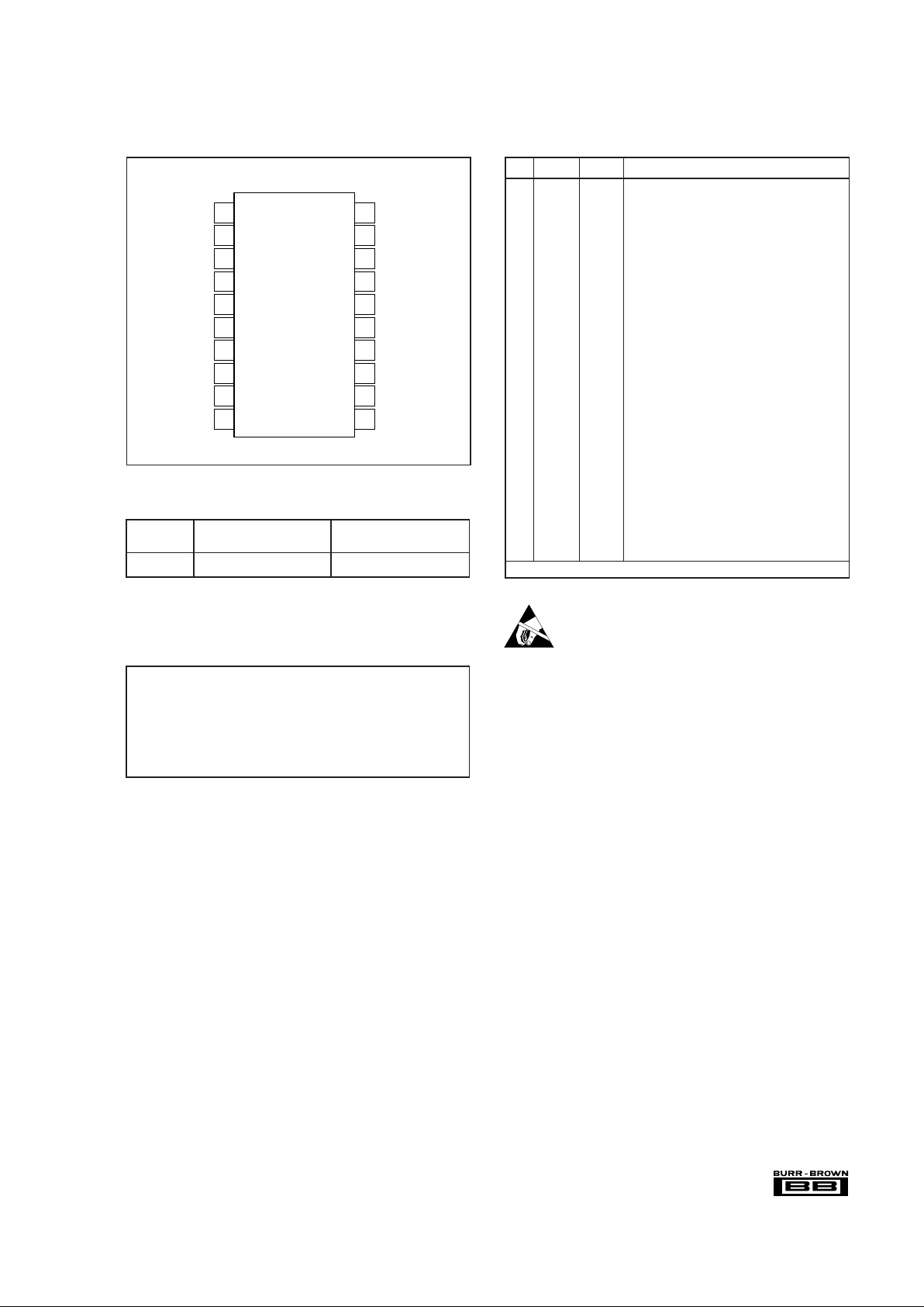
PIN ASSIGNMENTS
PIN NAME TYPE FUNCTION
1 NC — No Connection.
2 SCKI IN System Clock Input: 256f
S
or 384fS.
3 TEST OUT Reserved for Factory Use.
4* ML IN Latch Enable for Serial Control Data.
5* MC IN Clock for Serial Control Data.
6* MD IN Data Input for Serial Control.
7* RSTB IN Reset Input. When this pin is low, the digital
filters and modulators are held in reset.
8 ZERO OUT Zero Data Flag. This pin is low when the data is
continuously zero for more than 65,535 cycles of
BCKIN.
9V
OUT
R OUT Right Channel Analog Output.
10 AGND PWR Analog Ground.
11 V
CC
PWR Analog Power Supply (+5V).
12 V
OUT
L OUT Left Channel Analog Output.
13 CAP — Common Pin for Analog Output Amplifiers.
14* BCKIN IN Bit Clock for Clocking in the Audio Data.
15* DIN IN Serial Audio Data Input.
16* LRCIN IN Left/Right Word Clock. Frequency is equal to fs.
17 GND PWR Ground.
18 NC — No Connection.
19 V
DD
PWR Digital Power Supply (+5V). Recommended con-
nection is to the analog power supply.
20 DGND PWR Digital Ground. Recommended connection is to
the digital ground plane.
* These pins include internal pull-up resistors.
PIN CONFIGURATION
TOP VIEW SSOP
PACKAGE INFORMATION
PACKAGE DRAWING
PRODUCT PACKAGE NUMBER
(1)
PCM1720 20-Pin SSOP 334-1
NOTE: (1) For detailed drawing and dimension table, please see end of data
sheet, or Appendix C of Burr-Brown IC Data Book.
ABSOLUTE MAXIMUM RATINGS
Power Supply Voltage.......................................................................+6.5V
+V
CC
to +VDD Difference ................................................................... ±0.1V
Input Logic Voltage ..................................................–0.3V to (V
DD
+ 0.3V)
Power Dissipation .......................................................................... 300mW
Operating Temperature Range .........................................–25°C to +85°C
Storage Temperature...................................................... –55°C to +125°C
Lead Temperature (soldering, 5s).................................................. +260°C
Thermal Resistance,
θ
JA
..............................................................+70°C/W
NC
SCKI
TEST
ML
MC
MD
RSTB
ZERO
V
OUT
R
AGND
DGND
V
DD
NC
GND
LRCIN
DIN
BCKIN
CAP
V
OUT
L
V
CC
1
2
3
4
5
6
7
8
9
10
20
19
18
17
16
15
14
13
12
11
ELECTROSTATIC
DISCHARGE SENSITIVITY
This integrated circuit can be damaged by ESD. Burr-Brown
recommends that all integrated circuits be handled with
appropriate precautions. Failure to observe proper handling
and installation procedures can cause damage.
ESD damage can range from subtle performance degradation
to complete device failure. Precision integrated circuits may
be more susceptible to damage because very small parametric
changes could cause the device not to meet its published
specifications.
Page 4
®
PCM1720
4
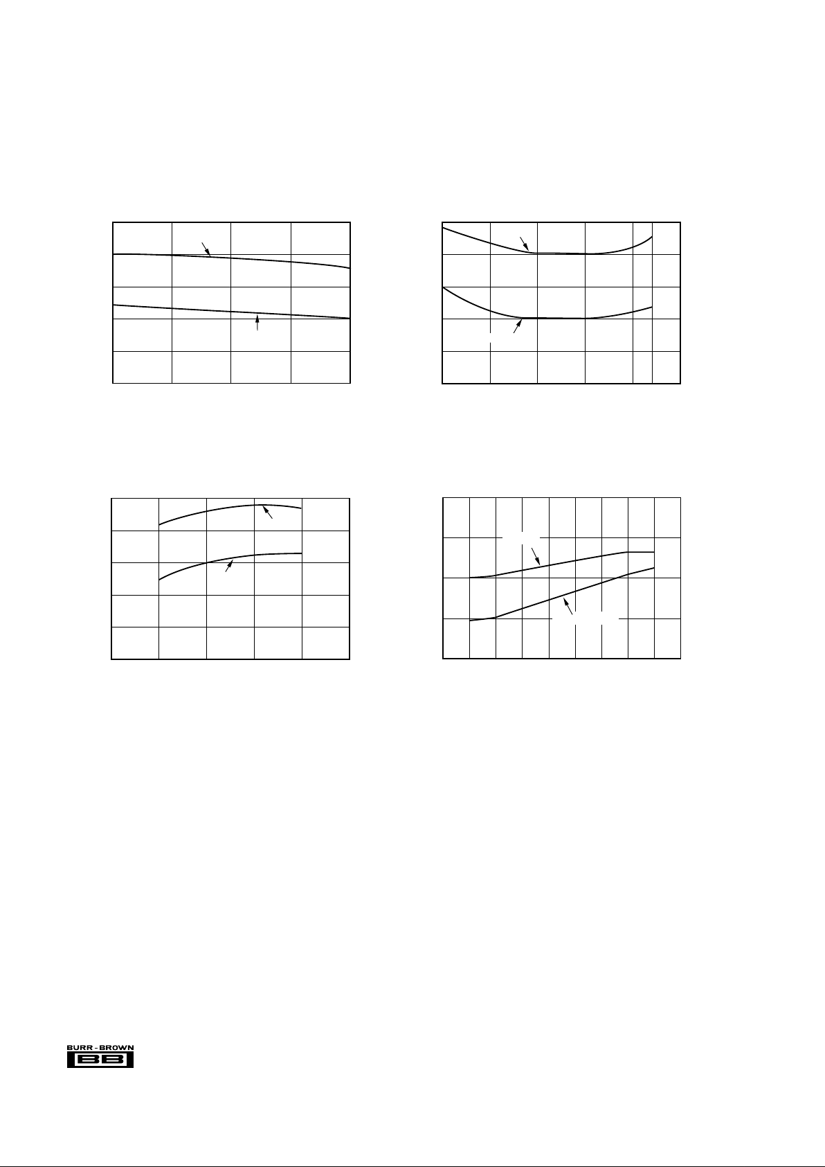
TYPICAL PERFORMANCE CURVES
At TA = +25°C, VCC = VDD = +5V, fS = 44.1kHz, 16-bit input data, unless otherwise noted. Measurement bandwidth is 20kHz
DYNAMIC PERFORMANCE
THD+N vs VCC, V
DD
VCC, VDD (V)
THD+N at FS (dB)
THD+N at –60dB (dB)
–84
–86
–88
–90
–92
–94
–30
–34
–38
4.5 5.0 5.5
f
S
= 96kHz
f
S
= 44.1kHz
DYNAMIC RANGE and SNR vs VCC, V
DD
VCC, V
DD
(dB)
100
98
96
94
92
90
3.5 4.0 4.5 5.0 5.5 6.0
SNR
Dynamic
Range
THD+N vs TEMPERATURE
Temperature (°C)
THD+N at FS (dB)
–84
–86
–88
–90
–92
–90
–25 0 25 50 75 85 100
f
S
= 96kHz
fS = 44.1kHz
THD+N and DYNAMIC RANGE vs f
S
Sampling Frequency, fS (kHz)
THD+N (dB)
Dynamic Range (dB)
–86
–88
–90
–92
–94
90
92
94
96
98
44.1 48 88.2 96
Dynamic Range
THD+N
Page 5

®
PCM1720
5
DE-EMPHASIS ERROR (3kHz)
0 3628 7256 10884 14512
0 4999.8375 9999.675 14999.5125 19999.35
0 5442 10884 16326 21768
Frequency (Hz)
0.6
0.4
0.2
0
–0.2
–0.4
–0.6
0.6
0.4
0.2
0
–0.2
–0.4
–0.6
0.6
0.4
0.2
0
–0.2
–0.4
–0.6
DE-EMPHASIS ERROR (44.1kHz)
Frequency (Hz)
DE-EMPHASIS ERROR (48kHz)
Frequency (Hz)
Error (dB) Error (dB) Error (dB)
PASSBAND RIPPLE CHARACTERISTIC
0
–0.2
–0.4
–0.6
–0.8
–1
0 0.1134f
S
0.2268f
S
0.3402f
S
0.4535f
S
dB
Frequency (Hz)
TYPICAL PERFORMANCE CURVES
At TA = +25°C, VCC = VDD = +5V, RL = 44.1kHz, f
SYS
= 384fS, and 16-bit input data, unless otherwise noted.
DIGITAL FILTER
0 0.4536fS1.3605fS2.2675fS3.1745fS4.0815f
S
0
–20
–40
–60
–80
–100
dB
OVERALL FREQUENCY CHARACTERISTIC
Frequency (Hz)
DE-EMPHASIS FREQUENCY RESPONSE (3kHz)
0 5k 10k 15k 20k 25k
Frequency (Hz)
0
–2
–4
–6
–8
–10
–12
DE-EMPHASIS FREQUENCY RESPONSE (44.1kHz)
0 5k 10k 15k 20k 25k
Frequency (Hz)
0
–2
–4
–6
–8
–10
–12
DE-EMPHASIS FREQUENCY RESPONSE (48kHz)
0 5k 10k 15k 20k 25k
Frequency (Hz)
0
–2
–4
–6
–8
–10
–12
Level (dB) Level (dB) Level (dB)
Page 6

®
PCM1720
6
FIGURE 1. “Normal” Data Input Timing.
FIGURE 2. “I2S” Data Input Timing.
FIGURE 3. Audio Data Input Timing.
14 15 16 1 2 3
14 15
1/fs
L_ch
R_ch
MSB LSB
16
LRCIN (pin 4)
BCKIN (pin 6)
AUDIO DATA WORD = 16-BIT
DIN (pin 5)
1 2 3
14 15
MSB LSB
16
18 19 20 1 2 3
18 19
MSB LSB
20
AUDIO DATA WORD = 20-BIT
DIN (pin 5)
1 2 3
18 19
MSB LSB
20
23 24 1 2 3
22 23
MSB LSB
24
AUDIO DATA WORD = 24-BIT
DIN (pin 5)
1 2 3
22 23
MSB LSB
24
1 2 3
14 15
1/fs
L_ch
R_ch
MSB LSB
16
LRCIN (pin 4)
BCKIN (pin 6)
AUDIO DATA WORD = 16-BIT
DIN (pin 5)
1 2 3
14 15
MSB LSB
16
1 2 3
18 19
MSB LSB
20
AUDIO DATA WORD = 20-BIT
DIN (pin 5)
1 2 3
18 19
MSB LSB
20
21
21
21
1 2 3
22 23
MSB LSB
24
AUDIO DATA WORD = 24-BIT
DIN (pin 5)
1 2 3
22 23
MSB LSB
24
LRCKIN
BCKIN
DIN
1.4V
1.4V
1.4V
t
BCH
t
BCL
t
LB
t
BL
t
DS
BCKIN Pulse Cycle Time
BCKIN Pulse Width High
BCKIN Pulse Width Low
BCKIN Rising Edge to LRCIN Edge
LRCIN Edge to BCKIN Rising Edge
DIN Set-up Time
DIN Hold Time
: t
BCY
: t
BCH
: t
BCL
: t
BL
: t
LB
: t
DS
: t
DH
: 100ns (min)
: 50ns (min)
: 50ns (min)
: 30ns (min)
: 30ns (min)
: 30ns (min)
: 30ns (min)
t
DH
t
BCY
Page 7

®
PCM1720
7
TYPICAL CONNECTION DIAGRAM
Figure 4 illustrates the typical connection diagram for
PCM1720 used in a stand-alone application.
SYSTEM CLOCK
The system clock for PCM1720 must be either 256f
S
or
384f
S
, where fS is the audio sampling frequency (LRCIN),
typically 32kHz, 44.1kHz or 48kHz. The system clock is
used to operate the digital filter and the noise shaper. The
system clock input (SCKI) is at pin 2.
PCM1720 has a system clock detection circuit which automatically detects the frequency, either 256f
S
or 384fS. The
system clock should be synchronized with LRCIN (pin 16),
but PCM1720 can compensate for phase differences. If the
phase difference between LRCIN and system clock is greater
than ±6 bit clocks (BCKIN), the synchronization is performed automatically. The analog outputs are forced to a
bipolar zero state (VCC/2) during the synchronization function. Table I shows the typical system clock frequency
inputs for the PCM1720.
FIGURE 4. Typical Connection Diagram.
SAMPLING SYSTEM CLOCK
RATE (LRCIN) FREQUENCY (MHz)
256f
S
384f
S
32kHz 8.192 12.288
44.1kHz 11.2896 16.9340
48kHz 12.288 18.432
TABLE I. System Clock Frequencies vs Sampling Rate.
SPECIAL FUNCTIONS
PCM1720 includes several special functions, including digital attenuation, digital de-emphasis, soft mute, data format
selection and input word resolution. These functions are
controlled using a three-wire interface. MD (pin 6) is used
for the program data, MC (pin 5) is used to clock in the
program data, and ML (pin 4) is used to latch in the program
data. Table II lists the selectable special functions.
FUNCTION DEFAULT MODE
Input Audio Data Format Selection
Normal Format Normal Format
I
2
S Format
Input Audio Data Bit Selection
16/20/24 Bits 16 Bits
Input LRCIN Polarity Selection
Lch/Rch = High/Low Lch/Rch = High/Low
Lch/Rch = Low/High
De-emphasis Control OFF
Soft Mute Control OFF
Attenuation Control 0dB
Lch, Rch Individually Lch, Rch Individually Fixed
Lch, Rch Common
Infinite Zero Detection Circuit Control OFF
Operation Enable (OPE) Enabled
Sample Rate Selection
Internal System Clock Selection
256f
S
384f
S
384f
S
Sampling Frequency
44.1kHz Group 44.1kHz
48kHz Group
32kHz Group
Analog Output Mode
L, R, Mono, Mute Stereo
TABLE II. Selectable Functions.
DIN
BCKIN
LRCIN
SCKI
15
14
16
2
4
5
6
7
ML
MC
MD
RSTB
12
13
20 19
9
8
10 11
PCM
Audio Data
Processor
256f
S
/384fS CLK
AGND
DGND
V
CC
+5V Analog
+5V Analog
V
DD
V
OUT
L
V
OUT
R
ZERO
CAP
PCM1720
+
10µF
Post
LPF
Post
LPF
Analog
Mute
Analog
Mute
STRB
SCKO
SDO
PIO
System
Controller
Rch Analog Out
Lch Analog Out
200Ω
Page 8

®
PCM1720
8
MAPPING OF PROGRAM REGISTERS
ATTENUATION DATA LOAD CONTROL, LCH
Bit 8 (LDL) is used to simultaneously set analog outputs of
Lch and Rch. An output level is controlled by AL[0:7]
attenuation data when this bit is set to 1. When set to 0, an
output level is not controlled and remains at the previous
attenuation level. A LDR bit in Register 1 has an equivalent
function as the LDL. When one of LDL or LDR is set to 1,
the output level of the left and right channel is simultaneously controlled. The attenuation level is given by:
ATT = 20 log (y/256) (dB), where y = x, when 0 ≤ x ≤ 254
y = x + 1, when x = 255
X is the user-determined step number, an integer value
between 0 and 255.
Example:
let x = 255
let x = 254
let x = 1
let x = 0
REGISTER 1 (A1 = 0, A0 = 1)
B15 B14 B13 B12 B11 B10 B9 B8 B7 B6 B5 B4 B3 B2 B1 B0
res res res res res A1 A0
LDR
AR7 AR6 AR5 AR4 AR3 AR2 AR1AR0
Register 1 is used to control right channel attenuation. As
in Register 1, bits 0 - 7 (AR0 - AR7) control the level of
attenuation.
B15 B14 B13 B12 B11 B10 B9 B8 B7 B6 B5 B4 B3 B2 B1 B0
REGISTER 0 res res res res res A1 A0 LDL AL7 AL6 AL5 AL4 AL3 AL2 AL1 AL0
REGISTER 1 res res res res res A1 A0 LDR AR7 AR6 AR5 AR4 AR3 AR2 AR1 AR0
REGISTER 2 res res res res res A1 A0 PL3 PL2 PL1 PL0 IW1 IW0 OPE DEM MUT
REGISTER 3 res res res res res A1 A0 IZD SF1 SF0 res res res ATC LRP I
2
S
PROGRAM REGISTER BIT MAPPING
PCM1720’s special functions are controlled using four program registers which are 16 bits long. These registers are all
loaded using MD. After the 16 data bits are clocked in, ML
is used to latch in the data to the appropriate register. Table
III shows the complete mapping of the four registers and
Figure 6 illustrates the data input timing.
ATT = 20log
255 +1
256
= 0dB
ATT = 20log
254
256
= –0.068 dB
ATT = 20log
1
256
= –48.16 dB
ATT = 20 log
0
256
= –∞
REGISTER 0 (A1 = 0, A0 = 0)
B15 B14 B13 B12 B11 B10 B9 B8 B7 B6 B5 B4 B3 B2 B1 B0
res res res res res A1 A0 LDL AL7 AL6 AL5 AL4 AL3 AL2 AL1 AL0
REGISTER BIT
NAME NAME DESCRIPTION
Register 0 AL (7:0) DAC Attenuation Data for Lch
LDL Attenuation Data Load Control for Lch
A (1:0) Register Address
res Reserved
Register 1 AR (7:0) DAC Attentuation Data for Rch
LDL Attenuation Data Load Control for Rch
A (1:0) Register Address
res Reserved
Register 2 MUT Left and Right DACs Soft Mute Control
DEM De-emphasis Control
OPE Left and Right DACs Operation Control
IW (1:0) Input Audio Data Bit Select
PL (3:0) Output Mode Select
A (1:0) Register Address
res Reserved
Register 3 I
2
S Audio Data Format Select
LRP Polarity of LRCIN (pin 7) Select
ATC Attenuator Control
SYS System Clock Select
SF (1:0) Sampling Rate Select
IZD Infinite Zero Detection Circuit Control
A (1:0) Register Address
res Reserved
Register 0 is used to control left channel attenuation. Bits
0 - 7 (AL0 - AL7) are used to determine the attenuation
level. The level of attenuation is given by:
ATT = [20 log10 (ATT_DATA/255)] dB
TABLE III. Internal Register Mapping.
Page 9

®
PCM1720
9
REGISTER 2 (A1 = 1, A0 = 0)
B15 B14 B13 B12 B11 B10 B9 B8 B7 B6 B5 B4 B3 B2 B1 B0
res res res res res A1 A0 PL3 PL2 PL1 PL0 IW1 IW0 OPE DEM MUTE
Register 2 is used to control soft mute, de-emphasis, operation enable, input resolution, and output format. Bit 0 is used
for soft mute: a “HIGH” level on bit 0 will cause the output
to be muted (this is ramped down in the digital domain, so
no “click” is audible). Bit 1 is used to control de-emphasis.
A “LOW” level on bit 1 disables de-emphasis, while a
“HIGH” level enables de-emphasis.
Bit 2, (OPE) is used for operational control. Table IV
illustrates the features controlled by OPE.
SOFTWARE MODE
DATA INPUT DAC OUTPUT INPUT
Zero Forced to BPZ
(1)
Enabled
Other Forced to BPZ
(1)
Enabled
Zero Controlled by IZD Enabled
Other Normal Enabled
OPE = 1
OPE = 0
TABLE IV. Output Enable (OPE) Function.
OPE controls the operation of the DAC: when OPE is
“LOW”, the DAC will convert all non-zero input data. If the
input data is continuously zero for 65, 536 cycles of BCKIN,
the output will be forced to zero only if IZD is “HIGH”.
When OPE is “HIGH”, the output of the DAC will be forced
to bipolar zero, irrespective of any input data.
IZD = 1
IZD = 0
DATA INPUT DAC OUTPUT
Zero Forced to BPZ
(1)
Other Normal
Zero Zero
(2)
Other Normal
TABLE V. Infinite Zero Detection (IZD) Function.
RSTB = “HIGH”
RSTB = “LOW”
SOFTWARE
MODE
DATA INPUT DAC OUTPUT INPUT
Zero
Controlled by OPE and IZD
Enabled
Other
Controlled by OPE and IZD
Enabled
Zero Forced to BPZ
(1)
Disabled
Other Forced to BPZ
(1)
Disabled
TABLE VI. Reset (RSTB) Function.
NOTE: (1) ∆∑ is disconnected from output amplifier. (2) ∆∑ is connected to
output amplifier.
Bits 3 (IW0) and 4 (IW1) are used to determine input word
resolution. PCM1720 can be set up for input word resolutions of 16, 20, or 24 bits:
Bit 4 (IW1) Bit 3 (IW0) Input Resolution
0 0 16-bit Data Word
0 1 20-bit Data Word
1 0 24-bit Data Word
0 0 Reserved
Bits 5, 6, 7, and 8 (PL0:3) are used to control output format.
The output of PCM1720 can be programmed for 16 different
states, as shown in Table VII.
PL0 PL1 PL2 PL3 Lch OUTPUT Rch OUTPUT NOTE
0 0 0 0 MUTE MUTE MUTE
0 0 0 1 MUTE R
0 0 1 0 MUTE L
0 0 1 1 MUTE (L + R)/2
0 1 0 0 R MUTE
0101 R R
0 1 1 0 R L REVERSE
0 1 1 1 R (L + R)/2
1 0 0 0 L MUTE
1 0 0 1 L R STEREO
1010 L L
1 0 1 1 L (L + R)/2
1 1 0 0 (L + R)/2 MUTE
1 1 0 1 (L + R)/2 R
1 1 1 0 (L + R)/2 L
1 1 1 1 (L + R)/2 (L + R)/2 MONO
TABLE VII. Programmable Output Format.
REGISTER 3 (A1 = 1, A0 = 1)
B15 B14 B13 B12 B11 B10 B9 B8 B7 B6 B5 B4 B3 B2 B1 B0
res res res res res A1 A0 IZD SF1 SF0 res res res ATC LRP I2S
Register 3 is used to control input data format and polarity,
attenuation channel control, system clock frequency, sampling frequency and infinite zero detection.
Bits 0 (I
2
S) and 1 (LRP) are used to control the input data
format. A “LOW” on bit 0 sets the format to “Normal”
(MSB-first, right-justified Japanese format) and a “HIGH”
sets the format to I
2
S (Philips serial data protocol). Bit 1
(LRP) is used to select the polarity of LRCIN (sample rate
clock). When bit 1 is “LOW”, left channel data is assumed
when LRCIN is in a “HIGH” phase and right channel data
is assumed when LRCIN is in a “LOW” phase. When bit
1 is “HIGH”, the polarity assumption is reversed.
Bit 2 (ATC) is used for controlling the attenuator. When
bit 2 is “HIGH”, the attenuation data loaded in program
Register 0 is used for both left and right channels. When
bit 2 is “LOW”, the attenuation data for each register is
applied separately to left and right channels.
Bits 6 (SF0) and 7 (SF1) are used to select the sampling
frequency:
SF1 SF0 Sampling Frequency
0 0 44.1kHz group 22.05/44.1/88.2kHz
0 1 48kHz group 24/48/96kHz
1 0 32kHz group 16/32/64kHz
1 1 Reserved Not Defined
Bit 8 is used to control the infinite zero detection function
(IZD).
Page 10

®
PCM1720
10
feature is used to avoid noise which may occur when the
input is DC. When the output is forced to bipolar zero,
there may be an audible click. PCM1720 allows the zero
detect feature to be disabled so the user can implement
external muting circuit.
When IZD is “LOW”, the zero detect circuit is off. Under
this condition, no automatic muting will occur if the input
is continuously zero. When IZD is “HIGH”, the zero detect
feature is enabled. If the input data is continuously zero for
65, 536 cycles of BCKIN, the output will be immediately
forced to a bipolar zero state (V
CC
/2). The zero detection
FIGURE 5. Serial Interface Timing.
B15 B14 B13 B12 B11 B10 B9 B8 B7 B6 B5 B4 B3 B2 B1 B0
ML (pin 4)
MC (pin 5)
MD (pin 6)
FIGURE 6. Program Register Input Timing.
1.4V
1.4V
1.4V
ML
MC
MD
MC Pulse Cycle Time
MC Pulse Width LOW
MC Pulse Width HIGH
MD Set-up Time
MC Hold Time
ML Low Level Time
ML Set-up Time
ML Hold Time
: t
MCY
: t
MCL
: t
MCH
: t
MDS
: t
MDH
: t
MLL
: t
MLS
: t
MLH
: 100ns (min)
: 50ns (min)
: 50ns (min)
: 30ns (min)
: 30ns (min)
: 30ns + 1SYSCLK (min)
: 30ns (min)
: 30ns (min)
t
MCY
t
MDS
t
MDH
t
MCHtMCL
t
MLS
t
MLH
t
MLL
Page 11

®
PCM1720
11
APPLICATION
CONSIDERATIONS
DELAY TIME
There is a finite delay time in delta-sigma converters. In A/D
converters, this is commonly referred to as latency. For a
delta-sigma D/A converter, delay time is determined by the
order number of the FIR filter stage, and the chosen sampling
rate. The following equation expresses the delay time of
PCM1720:
T
D
= 11.125 x 1/f
S
For fS = 44.1kHz, TD = 11.125/44.1kHz = 251.4µs
Applications using data from a disc or tape source, such as
CD audio, CD-Interactive, Video CD, DAT, Minidisc,
etc., generally are not affected by delay time. For some
professional applications such as broadcast audio for studios, it is important for total delay time to be less than 2ms.
OUTPUT FILTERING
For testing purposes all dynamic tests are done on the
PCM1720 using a 20kHz low pass filter. This filter limits
the measured bandwidth for THD+N, etc. to 20kHz. Failure
to use such a filter will result in higher THD+N and lower
SNR and Dynamic Range readings than are found in the
specifications. The low pass filter removes out of band
noise. Although it is not audible, it may affect dynamic
specification numbers.
The performance of the internal low pass filter from DC to
24kHz is shown in Figure 7. The higher frequency rolloff of
the filter is shown in Figure 8. If the user’s application has
the PCM1720 driving a wideband amplifier, it is recommended to use an external low pass filter. A simple 3rdorder filter is shown in Figure 9. For some applications, a
passive RC filter or 2nd-order filter may be adequate.
FIGURE 8. Low Pass Filter Wideband Frequency Response.
1.0
0.5
0
–0.5
–1.0
dB
20
Frequency (Hz)
100 1k 10k 24k
INTERNAL ANALOG FILTER FREQUENCY RESPONSE
(20Hz~24kHz, Expanded Scale)
FIGURE 7. Low Pass Filter Frequency Response.
10
5
0
–5
–10
–15
–20
–25
–30
–35
–40
–45
–50
–55
10 100 1k 10k 100k 1M 10M
Frequency (Hz)
dB
–60
INTERNAL ANALOG FILTER FREQUENCY RESPONSE
(10Hz~10MHz)
10kΩ
10kΩ
10kΩ
1500pF
100pF
680pF
+
V
SIN
–
90
0
–90
–180
–270
–360
100 1k 10k 100k 1M
GAIN vs FREQUENCY
Frequency (Hz)
Phase (°)
6
–14
–34
–54
–74
–94
Gain (dB)
Gain
Phase
OPA604
FIGURE 9. 3rd-Order LPF.
Page 12

®
PCM1720
12
POWER SUPPLY
CONNECTIONS
PCM1720 has two power supply connections: digital (VDD)
and analog (V
CC
). Each connection also has a separate
ground. If the power supplies turn on at different times, there
is a possibility of a latch-up condition. To avoid this condition, it is recommended to have a common connection
between the digital and analog power supplies. If separate
supplies are used without a common connection, the delta
between the two supplies during ramp-up time must be less
than 0.6V.
An application circuit to avoid a latch-up condition is shown
in Figure 10.
FIGURE 11. 5-Level ∆Σ Modulator Block Diagram.
FIGURE 10. Latch-up Prevention Circuit.
DGND AGND
V
DD
V
CC
Digital
Power Supply
Analog
Power Supply
BYPASSING POWER SUPPLIES
The power supplies should be bypassed as close as possible
to the unit. Refer to Figure 13 for optimal values of bypass
capacitors. It is also recommended to include a 0.1µF ceramic capacitor in parallel with the 10µF tantalum capacitor.
3rd ORDER ∆Σ MODULATOR
Frequency (kHz)
Gain (–dB)
20
0
–20
–40
–60
–80
–100
–120
–140
–160
0 5 10 15 20 25
FIGURE 12. Quantization Noise Spectrum.
THEORY OF OPERATION
The delta-sigma section of PCM1720 is based on a 5-level
amplitude quantizer and a 3rd-order noise shaper. This
section converts the oversampled input data to 5-level deltasigma format. A block diagram of the 5-level delta-sigma
modulator is shown in Figure 11. This 5-level delta-sigma
modulator has the advantage of stability and clock jitter over
the typical one-bit (2-level) delta-sigma modulator.
The combined oversampling rate of the delta-sigma modulator and the internal 8X interpolation filter is 48f
S
for a
384f
S
system clock, and 64fS for a 256fS system clock. The
theoretical quantization noise performance of the 5-level
delta-sigma modulator is shown in Figure 12.
Out
48f
S
(384fS)
64f
S
(256fS)
In
8f
S
18-Bit
+
++
4
3
2
1
0
5-level Quantizer
+
–
+
Z
–1
+
–
+
Z
–1
+
+
Z
–1
Page 13

®
PCM1720
13
AC-3 APPLICATION
Figure 13 shows the typical circuit diagram for Dolby AC-3, 5.1 channel system.
FIGURE 13. Connection Diagram for a 6-Channel AC-3 Application.
15
14
16
2
SCKO
LRCKO
SERO_0
SERO_1
SERO_2
SYSCKI
BCKIN
LRCIN
DIN
SCKI
ML
MC
MD
RSTB
V
OUT
L
CAP
V
OUT
R
ZERO
Master Clock
Generator
or
PLL
Reset
µP
STRB
SCKO
SDO
+5V Analog
Post
Low Pass
Filter
10µF
+
Three-wire I/F
(Serial I/O)
3
20
PCM1720
PCM1720
PCM1721
19
DGND
AC-3
Audio
Decoder
V
DD
AGND V
CC
4
5
6
7
9
8
12
13
Analog
Mute
Analog Out
Post
Low Pass
Filter
Analog
Mute
Analog Out
Mute
Control
+5V Analog
10 11
200Ω
15
14
16
2
BCKIN
LRCIN
DIN
SCKI
ML
MC
MD
RSTB
V
OUT
L
CAP
V
OUT
R
ZERO
+5V Analog
Post
Low Pass
Filter
10µF
+
20 19
DGND V
DD
AGND
V
CC
4
5
6
7
9
8
12
13
Analog
Mute
Analog Out
Post
Low Pass
Filter
Analog
Mute
Analog Out
Mute
Control
+5V Analog
10 11
200Ω
17
16
18
BCKIN
LRCIN
DIN
SCKO
SCKI
MCKI
ML
MC
MD
V
OUT
L
CAP
V
OUT
R
ZERO
+5V Analog
Post
Low Pass
Filter
10µF
+
2223 21 3
DGNDPGND
VDDV
DP
AGND
RSTB
V
CC
6
7
8
9
11
10
14
15
2
4
1
Analog
Mute
Analog Out
Post
Low Pass
Filter
Analog
Mute
Analog Out
Mute
Control
+5V Analog
12 13
200Ω
19
+
10µF
+
3.3µF
10µF
+
3.3µF
+
10µF
+
3.3µF
+
 Loading...