

Page 1
INTEGRATED CIRCUITS
PCK2057
2
70 – 190 MHz I
C differential
1:10 clock driver
Product data
Supersedes data of 2001 May 09
File under Integrated Circuits, ICL03
2001 Jun 12
Page 2
Philips Semiconductors Product data
2
70 – 190 MHz I
C differential 1:10 clock driver
PCK2057
FEA TURES
•Optimized for clock distribution in DDR (Double Data Rate)
SDRAM applications supporting DDR 200/266/300/333
•Full DDR solution provided when used with PCK2002P or
PCK2002PL, and PCK2022RA
•1-to-10 differential clock distribution
•Very low jitter (< 100 ps)
•Operation from 2.2 V to 2.7 V AV
and 2.3 V to 2.7 V V
DD
DD
•SSTL_2 interface clock inputs and outputs
•HCSL to SSTL_2 input conversion
•Test mode enables buffers while disabling PLL
•Tolerant of Spread Spectrum input clock
•3.3 V I
•2.5 V I
2
C support with 3.3 V VDDI2C
2
C support with 2.5 V VDDI2C
•Form, fit, and function compatible with CDCV850
DESCRIPTION
The PCK2057 is a high-performance, low-skew, low-jitter zero delay
is tied to
DD
) to ten
buffer that distributes a differential clock input pair (CLK, CLK
differential pairs of clock outputs and one differential pair of
feedback clock outputs. The clock outputs are controlled by the
clock inputs (CLK, CLK
), the feedback clocks (FBIN, FBIN), the
2-line serial interface (SDA, SCL), and the analog power input
(AV
). The two-line serial interface (I2C) can put the individual
DD
output clock pairs in a high-impedance state. When AV
GND, the PLL is turned off and bypassed for test purposes.
The device provides a standard mode (100 kbits) I
2
C interface for
device control. The implementation is as a slave/receiver. The serial
inputs (SDA, SCL) provide integrated pull-up resistors (typically
100 kΩ).
Two 8-bit, 2-line serial registers provide individual enable control for
each output pair. All outputs default to enabled at power-up. Each
output pair can be placed in a high-impedance mode, when a
low-level control bit is written to the control register. The registers
must be accessed in sequential order (i.e., random access of the
registers is not supported). The I
with either 2.5 V or 3.3 V (V
2
C interface circuit can be supplied
I2C).
DD
Since the PCK2057 is based on PLL circuitry, it requires a
stabilization time to achieve phase-lock of the PLL. This stabilization
time is required following power-up.
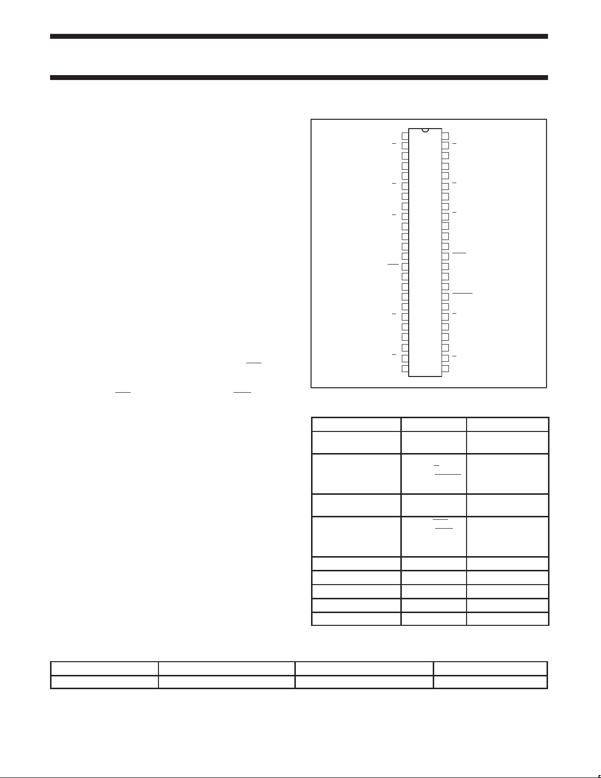
PIN CONFIGURATION
1
GND
Y
2
0
Y
3
0
4
V
DDQ
Y
5
1
Y
6
1
GND
7
8
GND
9
Y
2
Y
10
2
V
11
DDQ
SCL
12
13
CLK
14
CLK
VDDI2C
15
AV
16
DD
17
AGND
GND
18
Y
19
3
Y
20
3
21
V
DDQ
Y
22
4
Y
4
23
24
GND
PIN DESCRIPTION
PINS SYMBOL DESCRIPTION
1, 7, 8, 18, 24, 25, 31,
41, 42, 48
2, 3, 5, 6, 9, 10, 19, 20,
22, 23, 26, 27, 29, 30,
32, 33, 39, 40, 43, 44,
46, 47
4, 11, 21, 28, 34, 38,
45
13, 14, 35, 36 CLK, CLK,
16 AV
17 AGND Analog ground
37 SDA Serial data
12 SCL Serial clock
15 VDDI2C I2C power
FBOUT, FBOUT
48
GND
47
Y
5
Y
46
5
45
V
DDQ
Y
44
6
Y
6
43
GND
42
GND
41
Y
7
40
Y
39
7
V
DDQ
38
SDA
37
FBIN
36
FBIN
35
V
34
DDQ
FBOUT
33
FBOUT
32
GND
31
Y
8
30
Y
29
8
V
28
DDQ
Y
9
27
26
Y
9
GND
25
SW00506
GND Ground
Yn, Yn,
V
DDQ
FBIN, FBIN
DD
Buffered output
copies of input clock,
CLK
2.5 V supply
Differential clock
inputs and feedback
differential clock
inputs
Analog power
ORDERING INFORMATION
PACKAGES TEMPERATURE RANGE ORDER CODE DRAWING NUMBER
48-Pin Plastic TSSOP 0 to +70 °C PCK2057DGG SOT362-1
2001 Jun 12 853–2253 26485
2
Page 3
Philips Semiconductors Product data
2
70 – 190 MHz I
C differential 1:10 clock driver
PCK2057
FUNCTION TABLE
1
AV
DD
INPUTS OUTPUTS
CLK CLK Y Y FBOUT FBOUT
GND L H L H L H Bypassed/OFF
GND H L H L H L Bypassed/OFF
2.5 V (nom.) L H L H L H ON
2.5 V (nom.) H L H L H L ON
NOTES:
H = HIGH voltage level
L = LOW voltage level
1. Each output pair (except FBOUT and FBOUT
) can be put into a high-impedance state through the 2-line serial interface.
PLL ON/OFF
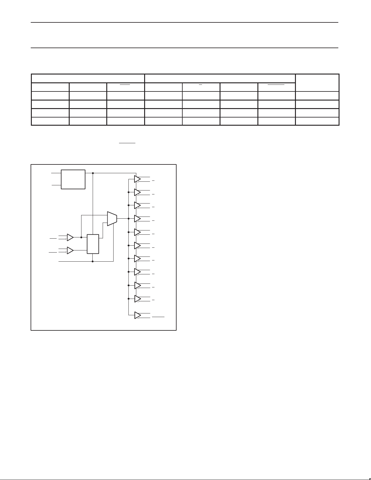
BLOCK DIAGRAM
SDA
SCL
CLK
CLK
FBIN
FBIN
AV
DD
CONTROL
LOGIC
PLL
Y
0
Y
0
Y
1
Y
1
Y
2
Y
2
Y
3
Y
3
Y
4
Y
4
Y
5
Y
5
Y
6
Y
6
Y
7
Y
7
Y
8
Y
8
Y
9
Y
9
FBOUT
FBOUT
SW00507
2001 Jun 12
3
Page 4

Philips Semiconductors Product data
2
70 – 190 MHz I
C differential 1:10 clock driver
PCK2057
I2C ADDRESS
11 0 1001
R/W
su01394
I2C CONSIDERA TIONS
I2C has been chosen as the serial bus interface to control the PCK2057. I2C was chosen to support the JEDEC proposal JC-42.5 168 Pin
Unbuffered SDRAM DIMM. All vendors are required to determine the legal issues associated with the manufacture of I
1) Address assignment: The clock driver in this specification uses the single, 7-bit address shown below. All devices can use the address if only
one master clock driver is used in a design. The address can be re-used for the CKBF device if no other conflicting I
the system.
The following address was confirmed by Philips on 09/04/96.
A6 A5 A4 A3 A2 A1 A0 R/W
11010010
NOTE: The R/W
bit is used by the I2C controller as a data direction bit. A ‘zero’ indicates a transmission (WRITE) to the clock device. A ‘one’
indicates a request for data (READ) from the clock driver. Since the definition of the clock buffer only allows the controller to WRITE data; the
bit of the address will always be seen as ‘zero’. Optimal address decoding of this bit is left to the vendor.
R/W
2) Data Transfer Rate: 100 kbits/s (standard mode) is the base functionality required. Fast mode (400 kbits/s) functionality is optional.
3) Logic Levels: I
2
C logic levels are based on a percentage of VDD for the controller and other devices on the bus. Assume all devices are
based on a 3.3 Volt supply.
4) Data Byte Format: Byte format is 8 Bits as described in the following appendices.
2
5) Data Protocol: To simplify the clock I
C interface, the clock driver serial protocol was specified to use only block writes from the controller.
The bytes must be accessed in sequential order from lowest to highest byte with the ability to stop after any complete byte has been
transferred. Indexed bytes are not allowed. However, the SMBus controller has a more specific format than the generic I
The clock driver must meet this protocol which is more rigorous than previously stated I2C protocol. Treat the description from the viewpoint of
controller. The controller “writes” to the clock driver.
2
C devices.
2
C clock driver is used in
2
C protocol.
1 bit 7 bits 1 1 8 bits 1
Start bit Slave Address R/W DUMMY DUMMY
Ack Data Byte 1Ack Data Byte 2 Ack StopAckAck
1 bit 8 bits 1 18 bits 1
SW00911
NOTE: The acknowledgement bit is returned by the slave/receiver (the clock driver).
2
6) Electrical Characteristics: All electrical characteristics must meet the standard mode specifications found in section 15 of the I
C
specification.
a) Pull-Up Resistors: Any internal resistors pull-ups on the SDATA and SCLOCK inputs must be stated in the individual datasheet. The use of
internal pull-ups on these pins of below 100 kΩ is discouraged. Assume that the board designer will use a single external pull-up resistor for
each line and that these values are in the 5–6 kΩ range. Assume one I
clock driver plus one/two more I
2
C devices on the platform for capacitive loading purposes.
2
C device per DIMM (serial presence detect), one I2C controller, one
(b) Input Glitch Filters: Only fast mode I2C devices require input glitch filters to suppress bus noise. The clock driver is specified as a standard
mode device and is not required to support this feature.
For specific I
2001 Jun 12
2
C information, consult the Philips I2C Peripherals Data Handbook IC12 (1997).
4
Page 5

Philips Semiconductors Product data
2
70 – 190 MHz I
C differential 1:10 clock driver
PCK2057
SERIAL CONFIGURATION MAP
The serial bits will be read by the clock buffer in the following order:
Byte 0 – Bits 7, 6, 5, 4, 3, 2, 1, 0
Byte 1 – Bits 7, 6, 5, 4, 3, 2, 1, 0
All unused register bits (Reserved and “—”) should be designed as “Don’t Care”. It is expected that the controller will force all of these bits to a
“0” level.
All register bits labeled “Initialize to 0” must be written to zero during initialization. Failure to do so may result in a higher than normal operating
current.
Byte 0: Active/inactive register
1 = enable; 0 = disable
BIT PIN# NAME INITIAL VALUE DESCRIPTION
7 2, 3 CLK0, CLK0 1 Enable/Disable Outputs
6 5, 6 CLK1, CLK1 1 Enable/Disable Outputs
5 9, 10 CLK2, CLK2 1 Enable/Disable Outputs
4 19, 20 CLK3, CLK3 1 Enable/Disable Outputs
3 22, 23 CLK4, CLK4 1 Enable/Disable Outputs
2 47, 46 CLK5, CLK5 1 Enable/Disable Outputs
1 44, 43 CLK6, CLK6 1 Enable/Disable Outputs
0 40, 39 CLK7, CLK7 1 Enable/Disable Outputs
NOTE:
1. Inactive means outputs are disabled from switching. These outputs are designed to be configured at power-on and are not expected to be
configured during the normal modes of operation.
Byte 1: Active/inactive register
1 = enable; 0 = disable
BIT PIN# NAME INITIAL VALUE DESCRIPTION
7 30, 29 CLK8, CLK8 1 Enable/Disable Outputs
6 27, 26 CLK9, CLK9 1 Enable/Disable Outputs
5 — — 0 Reserved
4 — — 0 Reserved
3 — — 0 Reserved
2 — — 0 Reserved
1 — — 0 Power-Down Mode Disable/Enable
0 — — 0 HCSL Enable/Disable
NOTE:
1. Inactive means outputs are disabled from switching. These outputs are designed to be configured at power-on and are not expected to be
configured during the normal modes of operation.
2001 Jun 12
5
Page 6

Philips Semiconductors Product data
SYMBOL
PARAMETER
TEST CONDITIONS
UNIT
V
Input voltage range
SYMBOL
PARAMETER
UNIT
IL
g
IH
g
V
g
IOLLOW-level output current
2
70 – 190 MHz I
C differential 1:10 clock driver
PCK2057
ABSOLUTE MAXIMUM RATINGS (see Note 1)
Over recommended operating conditions. V oltages are referenced to GND (ground = 0 V).
LIMITS
MIN MAX
V
/AV
DDQ
VDDI2C I2C supply voltage range 0.5 4.6 V
I
V
O
I
IK
I
OK
I
O
T
stg
NOTES:
1. Stresses beyond those listed under “absolute maximum ratings” may cause permanent damage to the device. These are stress ratings only,
and functional operation of the device at these or any other conditions beyond those indicated under “recommended operating conditions”
is not implied. Exposure to absolute-maximum-rated conditions for extended periods may affect device reliability .
2. The input and output negative voltage ratings may be exceeded if the input and output clamp-current ratings are observed.
3. This value is limited to 3.6 V maximum.
Supply voltage range 0.5 3.6 V
DD
p
except SCL and SDA see Notes 2 and 3 –0.5 V
SCL and SDA see Notes 2 and 3 –0.5 VDDI2C + 0.5 V
Output voltage range see Notes 2 and 3 –0.5 V
Input clamp current VI < 0 or VI > V
Output clamp current VO < 0 or VO > V
Continuous output current VO = 0 to V
Continuous current to GND or V
DDQ
DDQ
DDQ
DDQ
— ±50 mA
— ±50 mA
— ±50 mA
— ±100 mA
DDQ
DDQ
Storage temperature range –65 +150 °C
+ 0.5 V
+ 0.5 V
RECOMMENDED OPERATING CONDITIONS (see Note 1)
TEST
Supply voltage
V
AV
CONDITIONS
DDQ
DD
MIN TYP MAX
2.3 — 2.7 V
2.2 — 2.7 V
VDDI2C see Note 2 2.3 — 3.6 V
CLK, CLK,
HCSL buffer only
V
LOW-level input voltage
IL
CLK, CLK –0.3 — V
— 0 0.24 V
FBIN, FBIN — — V
SDA, SCL — — 0.3 × VDDI2C V
CLK, CLK,
HCSL buffer only
V
HIGH-level input voltage
IH
CLK, CLK 0.4 — V
FBIN, FBIN V
0.66 0.71 — V
/2 + 0.18 — — V
DDQ
SDA, SCL 0.7 × VDDI2C — — V
DC input signal voltage see Note 3 –0.3 — V
DC: CLK, FBIN see Note 4 0.36 — V
AC: CLK, FBIN see Note 4 0.2 — V
– VIL) — 0.55 × (V
IH
— — 12 mA
SDA — — 3 mA
V
I
OH
Differential input signal
ID
voltage
Input differential pair cross-voltage see Note 5 0.45 × (V
IX
HIGH-level output current — — –12 mA
p
SR Input slew rate see Figure 3 1 — 4 V/ns
SSC modulation frequency 30 — 33.3 kHz
SSC clock input frequency deviation 0 — –0.50 %
T
amb
Operating free-air temperature 0 — +70 °C
NOTES:
1. Unused inputs must be held HIGH or LOW to prevent them from floating.
2. All devices on the I
2
C-bus, with input levels related to VDDI2C, must have one common supply line to which the pull-up resistor is connected.
3. DC input signal voltage specifies the allowable DC execution of differential input.
4. Differential input signal voltage specifies the differential voltage |V
is the complementary input level.
5. Differential cross-point voltage is expected to track variations of V
– VCP| required for switching, where VTR is the true input level, and V
TR
and is the voltage at which the differential signals must be crossing.
DD
LIMITS
– 0.4 V
DDQ
/2 – 0.18 V
DDQ
+ 0.3 V
DDQ
+ 0.3 V
DDQ
+ 0.6 V
DDQ
+ 0.6 V
DDQ
– VIL) V
IH
CP
2001 Jun 12
6
Page 7

Philips Semiconductors Product data
SYMBOL
PARAMETER
TEST CONDITIONS
UNIT
VOHHIGH-level output voltage
LOW-level output voltage
I
SYMBOL
PARAMETER
UNIT
SYMBOL
PARAMETER
UNIT
2
70 – 190 MHz I
C differential 1:10 clock driver
PCK2057
DC ELECTRICAL CHARACTERISTICS
Over recommended operating conditions.
LIMITS
DDQ
1
/2 V
MAX
/2 + 0.2 V
DDQ
V
Input voltage All inputs V
IK
p
V
OL
p
SDA VDDI2C = 3.0 V; IOL = 3 mA — — 0.4 V
V
OX
I
I
OZ
DDPD
I
DD
AI
Output differential cross voltage V
Input current CLK, FBIN V
I
High impedance state output current V
Power-down current on V
+ AVDDCLK at 0 MHz; Σ of IDD and AI
DDQ
Power-down current on VDDI2C CLK at 0 MHz; V
Dynamic current on V
Supply current on AV
DD
DDQ
DD
IDDI2C Supply current on VDDI2C
C
Input capacitance V
I
NOTES:
1. All typical values are at respective nominal V
DDQ
V
DDQ
V
DDQ
DDQ
.
MIN TYP
= 2.3 V; II = –18 mA — — –1.2 V
DDQ
= min to max; IOH = –1 mA V
V
= 2.3 V; IOH = –12 mA 1.7 — — V
DDQ
= min to max; IOL = 1 mA — — 0.1 V
DDQ
V
= 2.3 V; IOL = 12 mA — — 0.6 V
DDQ
= 2.7 V; VI = 0 V to 2.7 V — — ±10 µA
DDQ
= 2.7 V; VO = V
or GND — — ±10 µA
DDQ
DD
= 3.6 V — 3 20 µA
DDQ
– 0.1 — — V
DDQ
/2 – 0.2 V
DDQ
— 150 250 µA
fO = 100 MHz — 205 230 mA
fO = 100 MHz — 4 6 mA
VDDI2C = 3.6 V;
SCL and SDA = 3.6V
= 2.5 V; VI = V
DDQ
or GND 2 2.8 3 pF
— 1 2 mA
TIMING REQUIREMENTS
Over recommended ranges of supply voltage and operating free-air temperature.
LIMITS
MIN MAX
f
CLK
Clock frequency 70 190 MHz
Input clock duty cycle 40 60 %
Stabilization time
1
— 100 µs
NOTE:
1. Time required for the integrated PLL circuit to obtain phase lock of its feedback signal to its reference signal. For phase lock to be obtained,
a fixed-frequency, fixed-phase reference signal must be present at CLK. Until phase lock is obtained, the specifications for propagation
delay, skew, and jitter parameters given in the switching characteristics table are not applicable. This parameter does not apply for input
modulation under SSC application.
TIMING REQUIREMENTS FOR THE I2C INTERFACE
Over recommended ranges of operating free-air temperature and VDDI2C from 3.3 V to 3.6 V..
STANDARD-MODE I2C-BUS
MIN MAX
f
SCL
t
BUF
t
SU;STA
t
HD;STA
t
LOW
t
HIGH
t
t
t
SU;DAT
t
HD;DAT
t
SU;STO
SCL clock frequency — 100 kHz
Bus free time between a STOP and ST ART condition 4.7 — µs
Set-up time for a repeated STAR T condition 4.7 — µs
Hold time (repeated) STAR T condition. After this period, the first clock is generated. 4.0 — µs
LOW period of the SCL clock 4.7 — µs
HIGH period of the SCL clock 4.0 — µs
Rise time of both SDA and SCL signals — 1000 ns
r
Fall time of both SDA and SCL signals — 300 ns
f
DATA set-up time 250 — ns
DATA hold time 0 — ns
Set-up time for STOP condition 4 — µs
2001 Jun 12
7
Page 8

Philips Semiconductors Product data
SYMBOL
PARAMETER
TEST CONDITIONS
UNIT
t
Static phase offset; see Figure 1
2
70 – 190 MHz I
C differential 1:10 clock driver
PCK2057
AC CHARACTERISTICS
LIMITS
MIN TYP MAX
t
PD
t
PHL
t
en
t
dis
t
jit(per)
t
jit(cc)
t
jit(hper)
∅
t
slr(o)
t
sk(o)
NOTE:
1. This time is for a PLL frequency of 100 MHz.
Propagation delay time Test mode/CLK to any output — 3.7 — ns
HIGH-to-LOW level propagation delay time SCL to SDA (acknowledge) — 500
1
— ns
Output enable time Test mode/SDA to Y output — 85 — ns
Output disable time Test mode/SDA to Y output — 35 — ns
Jitter (period); see Figure 4 100 MHz to 167 MHz –75 — 75 ps
Jitter (cycle-to-cycle); see Figure 5 100 MHz to 167 MHz –75 — 75 ps
Half-period jitter; see Figure 6 100 MHz to 167 MHz –90 — 90 ps
p
;
133 MHz/VID on CLK = 0.71 V 220 — 450 ps
167 MHz/VID on CLK = 0.71 V 140 — 270 ps
Output clock slew rate; see Figure 3 terminated with 120 Ω/14 pF 1 — 2 V/ns
Output skew; see Figure 2 — — 75 ps
SSC modulation frequency 30 — 33.3 kHz
SSC clock input frequency deviation 0.00 — –0.50 %
AC WAVEFORMS
FB
FB
CLK
CLK
IN
IN
, FB
Yx
Yx, FB
OUT
OUT
t
(O)n
t
(O)
n =N
t
Σ
=
(O)n
1
N
(N is a large number of samples)
t
(O)n + 1
SW00882
Figure 1. Static phase offset
Yx
Yx
t
sk(O)
2001 Jun 12
SW00883
Figure 2. Output skew
8
Page 9

Philips Semiconductors Product data
2
70 – 190 MHz I
C differential 1:10 clock driver
PCK2057
CLOCK INPUTS
AND OUTPUTS
Yx, FB
Yx, FB
Yx, FB
Yx, FB
OUT
OUT
OUT
OUT
80%
t
, t
SLR(I)
SLR(O)
Figure 3. Input and output slew rates
t
= t
JIT(PER)
cycle n
t
cycle n
1
f
t
SLR(I)
O
80%
VID, V
OD
20%20%
, t
SLR(O)
SW00886
1
–
f
O
SW00884
Yx, FB
Yx, FB
OUT
OUT
Figure 4. Period jitter
– t
t
cycle n + 1
cycle n+1
t
cycle n
t
JIT(CC)
= t
cycle n
Figure 5. Cycle-to-cycle jitter
SW00881
2001 Jun 12
9
Page 10

Philips Semiconductors Product data
2
70 – 190 MHz I
C differential 1:10 clock driver
Yx, FB
OUT
Yx, FB
OUT
t
half period n
t
JIT(HPER)
1
f
O
= t
half period n
t
half period n + 1
1
–
2*f
O
PCK2057
SW00885
Figure 6. Half-period jitter
TEST CIRCUIT
VDD/2
PCK2057
–V
/2
DD
C = 14 pf
Z = 60 Ω
Z = 60 Ω
C = 14 pf
–VDD/2
R = 10 Ω
R = 10 Ω
–V
/2
DD
Z = 50 Ω
Z = 50 Ω
Figure 7. Output load test measurement
SCOPE
V
TT
V
TT
NOTE: V
R = 50 Ω
R = 50 Ω
= GND
TT
SW00912
2001 Jun 12
10
Page 11

Philips Semiconductors Product data
2
70 – 190 MHz I
TSSOP48: plastic thin shrink small outline package; 48 leads; body width 6.1 mm SOT362-1
C differential 1:10 clock driver
PCK2057
2001 Jun 12
11
Page 12

Philips Semiconductors Product data
2
70 – 190 MHz I
C differential 1:10 clock driver
PCK2057
Purchase of Philips I2C components conveys a license under the Philips’ I2C patent
to use the components in the I2C system provided the system conforms to the
I2C specifications defined by Philips. This specification can be ordered using the
code 9398 393 40011.
Data sheet status
Product
Data sheet status
Objective data
Preliminary data
Product data
[1] Please consult the most recently issued datasheet before initiating or completing a design.
[2] The product status of the device(s) described in this data sheet may have changed since this data sheet was published. The latest information is available on the Internet at URL
http://www.semiconductors.philips.com.
[1]
status
Development
Qualification
Production
[2]
Definitions
This data sheet contains data from the objective specification for product development.
Philips Semiconductors reserves the right to change the specification in any manner without notice.
This data sheet contains data from the preliminary specification. Supplementary data will be
published at a later date. Philips Semiconductors reserves the right to change the specification
without notice, in order to improve the design and supply the best possible product.
This data sheet contains data from the product specification. Philips Semiconductors reserves the
right to make changes at any time in order to improve the design, manufacturing and supply.
Changes will be communicated according to the Customer Product/Process Change Notification
(CPCN) procedure SNW-SQ-650A.
Definitions
Short-form specification — The data in a short-form specification is extracted from a full data sheet with the same type number and title. For
detailed information see the relevant data sheet or data handbook.
Limiting values definition — Limiting values given are in accordance with the Absolute Maximum Rating System (IEC 134). Stress above one
or more of the limiting values may cause permanent damage to the device. These are stress ratings only and operation of the device at these or
at any other conditions above those given in the Characteristics sections of the specification is not implied. Exposure to limiting values for extended
periods may affect device reliability.
Application information — Applications that are described herein for any of these products are for illustrative purposes only. Philips
Semiconductors make no representation or warranty that such applications will be suitable for the specified use without further testing or
modification.
Disclaimers
Life support — These products are not designed for use in life support appliances, devices or systems where malfunction of these products can
reasonably be expected to result in personal injury . Philips Semiconductors customers using or selling these products for use in such applications
do so at their own risk and agree to fully indemnify Philips Semiconductors for any damages resulting from such application.
Right to make changes — Philips Semiconductors reserves the right to make changes, without notice, in the products, including circuits, standard
cells, and/or software, described or contained herein in order to improve design and/or performance. Philips Semiconductors assumes no
responsibility or liability for the use of any of these products, conveys no license or title under any patent, copyright, or mask work right to these
products, and makes no representations or warranties that these products are free from patent, copyright, or mask work right infringement, unless
otherwise specified.
Philips Semiconductors
811 East Arques Avenue
P.O. Box 3409
Sunnyvale, California 94088–3409
Telephone 800-234-7381
Copyright Philips Electronics North America Corporation 2001
All rights reserved. Printed in U.S.A.
Date of release: 06-01
Document order number: 9397 750 08476
2001 Jun 12
12
 Loading...