

Page 1

INTEGRATED CIRCUITS
PCK2023
CK408 (66/100/133/200 MHz)
spread spectrum differential system
clock generator
Product data
File under Integrated Circuits — ICL03
2001 Sep 07
Page 2
Philips Semiconductors Product data
CK408 (66/100/133/200 MHz) spread spectrum
differential system clock generator
FEA TURES
•3.3 V operation
•Three differential CPU clock pairs
•Ten PCI clocks at 3.3 V
•Six 66 MHz clocks at 3.3 V
•Two 48 MHz clocks at 3.3 V
•One 14.318 MHz reference clock
•66,100, 133 or 200 MHz operation
•Power management control pins
•CPU clock skew less than 200 ps cycle-to-cycle
•CPU clock skew less than 150 ps pin-to-pin
•1.5 ns to 3.5 ns delay on PCI pins
•Spread Spectrum capability
DESCRIPTION
The PCK2023 is a clock synthesizer/driver for a Pentium IV and
other similar processors.
The PCK2023 has three differential pair CPU current source
outputs. There are ten PCI clock outputs running at 33 MHz and two
48 MHz clocks. There are six 3V66 outputs. Finally, there is one
3.3 V reference clock at 14.318 MHz. All clock outputs meet Intel’s
drive strength, rise/fall times, jitter, accuracy, and skew
requirements.
The part possesses a dedicated power-down input pin for power
management control. This input is synchronized on-chip and
ensures glitch-free output transitions.
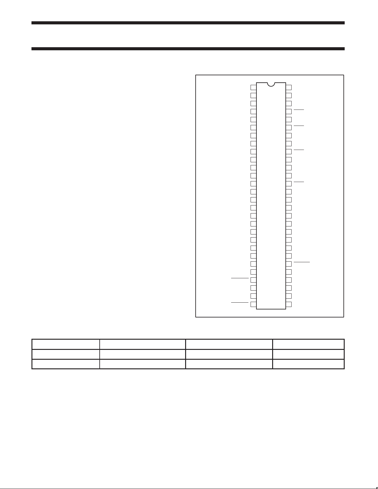
PIN CONFIGURATION
XTAL_In
XTAL_Out
V
PCIF0
PCIF1
PCIF2
V
V
PCI0
PCI1
V
V
PCI4
PCI5
PCI6
V
V
66Buff0/3V66_2
66Buff1/3V66_3
66Buff2/3V66_4
66In/3V66_5
PWRDWN
VDDA
1
DD
2
3
4
SS
5
6
7
8
DD
9
SS
10
11
12 45
13
14
DD
15
SS
16
17
18 39
19 38
DD
20
SS
21
22
23
24
25 32
26 31 V
27 30 SCLKVSSA
28 29Vtt_Pwrgd SDATA
PCK2023
REF_0
56V
S0
55
CPU3
54
CPU3
53
52
CPU0
51
CPU0
50
V
DD
CPU1
49
48
CPU1
47
V
SS
46
V
DD
CPU2PCI2
44PCI3
CPU2
Mult0
43
42
IREF
V
Iref
41
SS
40
S2
USB 48 MHz
DOT 48 MHz
37
48 MHz
V
DD
36
V
48 MHz
SS
35
3V66_1/VCH
34
PCI_Stop
33
3V66_0
V
DD
SS
SW00695
ORDERING INFORMATION
PACKAGES TEMPERATURE RANGE ORDER CODE DRAWING NUMBER
56-Pin Plastic SSOP 0 to +70 °C PCK2023DL SOT371-1
56-Pin Plastic TSSOP 0 to +70 °C PCK2023DGG SOT364-1
Intel and Pentium are registered trademarks of Intel Corporation.
2001 Sep 07 853-2278 27052
2
Page 3

Philips Semiconductors Product data
CK408 (66/100/133/200 MHz) spread
spectrum differential system clock generator
PIN DESCRIPTION
PIN NUMBER SYMBOL FUNCTION
56 ref 3.3 V 14.318 MHz clock output.
2 XTAL_In 14.318 MHz crystal input.
3 XTAL_Out 14.318 MHz crystal output.
44, 45, 48, 49, 51, 52
33 3V66_0 3.3 V 66 MHz clock output.
35 3V66_1/VCH 3.3 V selectable through I2C to be 66 MHz or 48 MHz
24 66In/3V66_5 66 MHz input to buffered 66Buff and PCI or 66 MHz clock from internal VCO.
21, 22, 23 66Buff [2:0] / 3V66 [4:2] 66 MHz buffered outputs from 66 input or 66 MHz clocks from internal VCO.
5, 6, 7
10, 11, 12, 13, 16, 17,
18
39 USB Fixed 48 MHz clock output.
38 DOT Fixed 48 MHz clock output.
40 S2 Special 3.3 V 3 level input for mode selection.
54, 55 S1, S0 3.3 V LVTTL inputs for CPU frequency selection.
42 I
43 Mult0 3.3 V LVTTL input for selecting the current multiplier for the CPU outputs.
25 PWRDWN 3.3 V L VTTL input for PowerDown active low.
34 PCI_Stop 3.3 V LVTTL input for PCI_Stop active low.
53 CPU_Stop 3.3 V L VTTL input for CPU_Stop active low.
28 Vtt_Pwrgd
29 SDATA I2C compatible SDATA.
30 SCLOCK I2C compatible SCLOCK.
1, 8, 14, 19, 32, 37, 46,
50
26 VDDA 3.3 V power supply for PLL.
4, 9, 15, 20, 31, 36, 41,
47
27 VSSA Ground for PLL.
CPU & CPU
[2:0]
PCIF
[2:0]
PCI
[6:0]
ref
V
DD
V
SS
Differential CPU clock outputs.
33 MHz clocks divided down from 66 input or divided down from 3V66.
PCI clock outputs divided down from 66 input or divided down from 3V66.
A precision resistor is attached to this pin which is connected to the internal current
reference.
3.3 V LVTTL input is a level sensitive strobe used to determine when S [2:0] and Mult0
inputs are valid and ok to be sampled (active low).
3.3 V power supply for outputs.
Ground for outputs.
PCK2023
2001 Sep 07
3
Page 4
Philips Semiconductors Product data
CK408 (66/100/133/200 MHz) spread
spectrum differential system clock generator
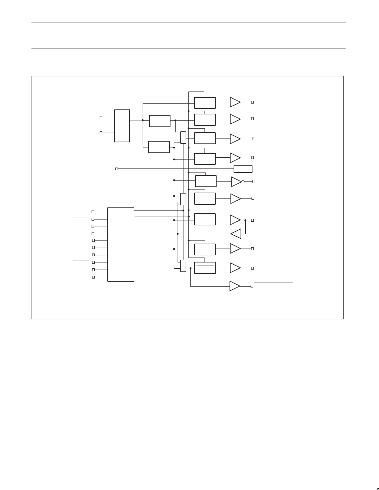
BLOCK DIAGRAM
XIN
XOUT
X
14.318
MHZ
IREF
OSC
X
X
USBPLL
SYSPLL
PWRDWN
PWRDWN
PWRDWN
PWRDWN
PWRDWN
PWRDWN
IBIAS
REF [0](14.318 MHz)
X
X
DOT/USB 48 MHz
3V66_1/VCH(48/66 MHz)
X
CPU [0–2](100/133 MHz)
X
CPU [0–2](100/133 MHz)
X
3V66 [2–4] (66 MHz)
X
PCK2023
CPU STOP
PCI STOP
PWRDWN
MULT0
Pwrgd
V
tt
SDA
SCL
X
X
X
S2
X
S1
X
S0
X
X
X
X
X
LOGIC
PWRDWN
PWRDWN
PWRDWN
66ln/3V66_5(66 MHz)
X
3V66_0 (66 MHz)
X
PCI [0–6](33 MHz)
X
PCIF [0–2] (33 MHz)
X
SW00861
2001 Sep 07
4
Page 5

Philips Semiconductors Product data
CK408 (66/100/133/200 MHz) spread
PCK2023
spectrum differential system clock generator
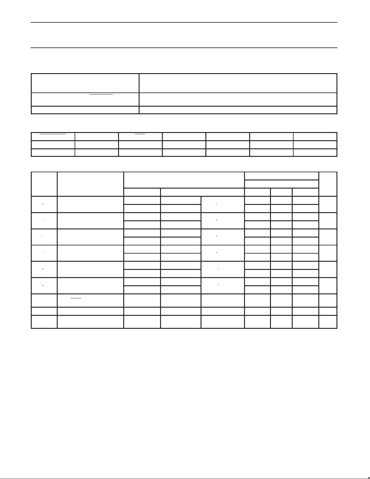
FREQUENCY SELECT/FUNCTION TABLE
S2 S1 S0 CPU 3V66
66BUFF/
3V66
1 0 0 66 MHz 66 MHz 66 In 66 input 66 In/2 14.318 MHz 48 MHz 66/48 MHz
1 0 1 100 MHz 66 MHz 66 In 66 input 66 In/2 14.318 MHz 48 MHz 66/48 MHz
1 1 0 200 MHz 66 MHz 66 In 66 input 66 In/2 14.318 MHz 48 MHz 66/48 MHz
1 1 1 133 MHz 66 MHz 66 In 66 input 66 In/2 14.318 MHz 48 MHz 66/48 MHz
0 0 0 66 MHz 66 MHz 66 MHz 66 MHz 33 MHz 14.318 MHz 48 MHz 66/48 MHz
0 0 1 100 MHz 66 MHz 66 MHz 66 MHz 33 MHz 14.318 MHz 48 MHz 66/48 MHz
0 1 0 200 MHz 66 MHz 66 MHz 66 MHz 33 MHz 14.318 MHz 48 MHz 66/48 MHz
0 1 1 133 MHz 66 MHz 66 MHz 66 MHz 33 MHz 14.318 MHz 48 MHz 66/48 MHz
Mid 0 0 Low Hi Z Hi Z Hi Z Hi Z Hi Z Hi Z Hi-Z
Mid 0 1 Tclk/2 Tclk/4 Tclk/4 Tclk/4 Tclk/8 Tclk Tclk/2 Tclk/4
NOTE:
1. Mid is defined as a voltage level between 1.0 V and 1.8 V for 3 level input functionality. Low is below 0.8 V. High is above 2.0 V.
2. 3V66_1/VCH output frequency is set by the I
2
C.
3. Frequency of the 48 MHz outputs must be +167 ppm to match USB default.
4. Rref output min = 14.316 MHz, nominal = 14.31818, max = 14.32 MHz.
5. Tclk is a test clock over-driven on the XTAL_In input during test mode.
66In/
3V66_5
PCIF/PCI REF 0 USB/DOT
3V66_1/
VCH
POWER DOWN MODE
PWRDWN CPU CPU 3V66
1 Normal Normal Normal Normal Normal Normal Normal Normal Normal
0 I
*2 Float Low Low Low Low Low Low Low
ref
HOST SWING SELECT FUNCTIONS – CK408
MULT 0
0 50 Ω R
1 50 Ω R
CONDITIONS CONFIGURATION LOAD MIN. MAX.
I
OUT
I
OUT
VDD = 3.3 V All combinations,
VDD = 3.3 V ±5% All combinations,
BOARD
IMPEDANCE
Nominal test load for given configuration –7% of I
see Table above
Nominal test load for given configuration –12% of I
see Table above
66BUFF/
I
= 221.1%
ref
I
= 5.00 mA
ref
= 475.1%
ref
I
= 2.32 mA
ref
3V66
ref
66In/
3V66_5
PCIF/PCI REF 0 USB/DOT
I
OH
IOH = 4*I
IOH = 6*I
ref
ref
See Table above
OH
See Table above
OH
VOH @ 50 W
1.0 V
0.7 V
See Table above
See Table above
+7% of I
+12% of I
3V66_1/
VCH
OH
OH
2001 Sep 07
5
Page 6

Philips Semiconductors Product data
SYMBOL
PARAMETER
CONDITION
UNIT
SYMBOL
PARAMETER
CONDITIONS
UNIT
NOTES
CK408 (66/100/133/200 MHz) spread
PCK2023
spectrum differential system clock generator
ABSOLUTE MAXIMUM RATINGS
V
DD3
I
IK
V
I
I
OK
V
O
I
O
T
stg
P
tot
NOTES:
1. Stresses beyond those listed may cause permanent damage to the device. These are stress ratings only and functional operation of the
device at these or any other conditions beyond those indicated under “Recommended Operating Conditions” is not implied. Exposure to
absolute-maximum-rated conditions for extended periods may affect device reliability .
2. The input and output voltage ratings may be exceeded if the input and output current ratings are observed.
DC 3.3 V supply –0.5 +4.6 V
DC input diode current VI < 0 — –50 mA
DC input voltage Note 2 — — V
DC output diode current VO > VDD or VO < 0 — ±50 mA
DC output voltage Note 2 –0.5 VDD + 0.5 V
DC output source or sink current VO = 0 to V
Storage temperature range –65 +150 °C
Power dissipation per package
plastic medium-shrink (SSOP)
DC OPERA TING CONDITIONS
V
DD3
AV
V
IH
V
IL
V
OL3
V
OH3
I
IL
f
ref
C
IN
C
XTAL
C
OUT
L
PIN
T
amb
NOTES:
1. Input leakage current does not include inputs with pull up or pull down resistors.
2. This is a recommendation, not an absolute requirement.
3. As seen by the crystal. Device is intended to be used with a 17–20 pF AT crystal.
DC 3.3 V supply voltage 3.135 3.465 V
DC 3.3 V analog supply voltage 3.135 3.465 V
DD
3.3 V input high voltage 2.0 VDD + 0.3 V
3.3 V input high voltage VSS – 0.3 0.8 V
3.3 V input low voltage IOL = 1.0 mA — 0.4 V
3.3 V input high voltage IOH = 1.0 mA 2.4 — V
Input leakage current 0 < VIN < V
reference frequency , oscillator normal value 14.31818 14.31818 MHz
Input pin capacitance — 5 pF 2
Xtal pin capacitance 13.5 22.5 pF 3
Output pin capacitance — 6 pF 2
Pin inductance — 7 nH 2
Operating ambient temperature range in free
air
1, 2
DD
For temperature range: –40 to +125°C
above +55°C derate linearly with 11.3 mW/K
DD
LIMITS
MIN MAX
— ±50 mA
— 850 mW
LIMITS
MIN MAX
–5 +5 µA 1
0 +70 °C
2001 Sep 07
6
Page 7
Philips Semiconductors Product data
TEST CONDITIONS
IOH48 MHz USB, VCH
y
mA
IOL48 MHz USB, VCH
y
mA
IOH48 MHz DOT
y
mA
IOL48 MHz DOT
y
mA
I
,, ,
y
mA
I
,, ,
y
mA
CK408 (66/100/133/200 MHz) spread
PCK2023
spectrum differential system clock generator
POWER MANAGEMENT
MAXIMUM 3.3 V SUPPLY CONSUMPTION
CONDITION
Power-down mode (PWRDWN = 0) 25 mA @ I
MAXIMUM DISCRETE CAP LOADS, V
ALL STATIC INPUTS = V
46 mA @ I
= 2.32 mA
ref
= 5.0 mA
ref
DD3
Full active 280 mA
CPU STOP FUNCTIONALITY
CPU_STOP CPU CPU 3V66 66BUFF PCIF/PCI USB/DOT
1 Normal Normal 66 MHz 66 input 66 input/2 48 MHz
0 I
*2 Float 66 MHz 66 input 66 input/2 48 MHz
ref
DC CHARACTERISTICS
SYMBOL PARAMETER
VDD (V) OTHER MIN TYP MAX
3.135 V
3.465 V
3.135 V
3.465 V
3.135 V
3.465 V
3.135 V
3.465 V
REF, PCI, PCIF,
OH
3V66, 66BUFF
REF, PCI, PCIF,
OL
3V66, 66BUFF
V
±I
CPU/CPU VSS = 0.0
OL
±I
Input leakage current 3.365 0 < VIN < V
I
3-State output OFF-State
OZ
current
3.135 V
3.465 V
3.135 V
3.465 V
3.465
NOTE:
1. All clock outputs loaded with maximum lump capacitance test load specified in AC characteristics section.
= 1.0 V
OUT
= 3.135 V
OUT
= 1.95 V
OUT
= 0.4 V
OUT
= 1.0 V
OUT
= 3.135 V
OUT
= 1.95 V
OUT
= 0.4 V
OUT
= 1.0 V
OUT
= 3.135 V
OUT
= 1.95 V
OUT
= 0.4 V
OUT
RS = 33.2 Ω
RP= 49.9 Ω
V
=
OUT
V
or GND
DD
DD3
Type 3A
12–60 Ω
Type 3A
12–60 Ω
Type 3B
12–60 Ω
Type 3B
12–60 Ω
Type 5
12–55 Ω
Type 5
12–55 Ω
–29 — —
— — –23
29 — —
— — 27
–29 — —
— — –23
29 — —
— — 27
–33 — —
— — –33
30 — —
— — 38
Type X1 0.0 — 0.05 V
— –5 — 5 µA
IO = 0 — — 10 µA
= 3.465 V
DDL
OR V
SS
LIMITS
T
= 0 to +70 °C UNIT
amb
2001 Sep 07
7
Page 8
Philips Semiconductors Product data
CK408 (66/100/133/200 MHz) spread
spectrum differential system clock generator
AC CHARACTERISTICS
V
= 3.3 V –5%; f
DD3
3V66 66 MHz TIMING REQUIREMENTS
SYMBOL PARAMETER
T
PERIOD
t
HIGH
t
LOW
t
RISE
t
FALL
t
JITTER
Edge rate rising edge rate 1.0 4.0 V/ns 12
Edge rate falling edge rate 1.0 4.0 V/ns 12
t
SKEW
t
SKEW
t
SKEW
= 14.31818 MHz
crystal
LIMITS
T
= 0 to +70 °C
amb
UNIT NOTES
MIN MAX
period 15.0 15.3 ns 8, 13
HIGH time 4.95 N/A ns 9
LOW time 4.55 N/A ns 10
rise time 0.5 2.0 ns 12
fall time 0.5 2.0 ns 12
cycle-to-cycle jitter — 250 ps
pin-to-pin skew 3V66 [1:0] 0.0 250 ps
pin-to-pin skew 3V66 [5:2] 0.0 250 ps
pin-to-pin skew 3V66 [5:0] 0.0 450 ps
PCK2023
66 MHz BUFFERED TIMING REQUIREMENTS
LIMITS
T
= 0 to +70 °C
SYMBOL PARAMETER
amb
UNITS NOTES
MIN MAX
t
RISE
t
FALL
t
PD
propagation delay from 66In to 66BUFF [2:0] 2.5 4.5 ns
rise time 0.5 2.0 ns 12
fall time 0.5 2.0 ns 12
Edge rate rising edge rate 1.0 4.0 V/ns 12
Edge rate falling edge rate 1.0 4.0 V/ns 12
t
SKEW
66 MHz buffered pin-to-pin skew 0.0 175 ps
PCIF/PCI AC TIMING REQUIREMENTS
LIMITS
T
= 0 to +70 °C
SYMBOL PARAMETER
T
PERIOD
t
HIGH
t
LOW
t
RISE
t
FALL
t
JITTER
period 30.0 N/A ns 8, 13
HIGH time 12.0 N/A ns 9
LOW time 12.0 N/A ns 10
rise time 0.5 2.0 ns 12
fall time 0.5 2.0 ns 12
cycle-to-cycle jitter — — ps
Edge rate rising edge rate 1.0 4.0 V/ns 12
Edge rate falling edge rate 1.0 4.0 V/ns 12
t
SKEW
t
PCI
pin-to-pin skew 0.0 500 ps
3V66 [5:0] leads 33 MHz PCI 1.5 3.5 ns
amb
MIN MAX
UNITS NOTES
2001 Sep 07
8
Page 9
Philips Semiconductors Product data
CK408 (66/100/133/200 MHz) spread
spectrum differential system clock generator
USB 48 MHz AC TIMING REQUIREMENTS
SYMBOL PARAMETER
T
DOT 48 MHz AC TIMING REQUIREMENTS
T
(average) period nominal = 20.829 ns
PERIOD
t
HIGH
t
LOW
HIGH time 8.094 10.036 ns
LOW time 7.694 9.836 ns
f frequency 48.000 48.008 MHz 8
t
RISE
t
FALL
t
JITTER
rise time 1.0 2.0 ns 12
fall time 1.0 2.0 ns 12
cycle-to-cycle jitter 0 350 ps
Edge rate rising edge rate 1.0 2.0 V/ns
Edge rate falling edge rate 1.0 2.0 V/ns
SYMBOL PARAMETER
(average) period nominal = 20.829 ns
PERIOD
t
HIGH
t
LOW
HIGH time 8.094 10.036 ns
LOW time 7.694 9.836 ns
f frequency 48.000 48.008 MHz 8
t
RISE
t
FALL
t
JITTER
rise time 0.5 1.0 ns 12
fall time 0.5 1.0 ns 12
cycle-to-cycle jitter — 350 ps
Edge rate rising edge rate 2.0 4.0 V/ns
Edge rate falling edge rate 2.0 4.0 V/ns
t
SKEW
USB to DOT — 1000 ps
LIMITS
T
= 0 to +70 °C
amb
MIN MAX
LIMITS
T
= 0 to +70 °C
amb
MIN MAX
PCK2023
UNITS NOTES
UNITS NOTES
2001 Sep 07
9
Page 10

Philips Semiconductors Product data
SYMBOL
PARAMETER
UNITS
NOTES
CK408 (66/100/133/200 MHz) spread
PCK2023
spectrum differential system clock generator
CPU 0.7 V AC TIMING REQUIREMENTS
CPU 200 MHz CPU 133 MHz CPU 100 MHz CPU 66 MHz
MIN MAX MIN MAX MIN MAX MIN MAX
T
PERIOD
t
ABSMIN
t
RISE
t
FALL
∆t
RISE
∆t
FALL
V
CROSS
∆V
CROSS
Total
∆V
CROSS
t
CCJITTER
Duty Cycle 45 55 45 55 45 55 45 55 % 7
Overshoot
Undershoot
t
SKEW
average period 5.0 5.1 7.5 7.65 10.0 10.2 15.0 15.3 ns 1, 7
absolute
minimum host
clock period
rise time 175 600 175 600 175 600 175 600 ps 2, 7, 14
fall time 175 600 175 600 175 600 175 600 ps 2, 7, 14
rise time
variation
fall time
variation
absolute
crossing point
voltages
total variation
of V
rising edge of
total variation
of V
over all edges
cycle-to-cycle
allowed at
allowed at
for
CROSS
host
CROSS
jitter
maximum
voltage
output
minimum
voltage
output
pin-to-pin — 150 — 150 — 150 — 150 ps
4.8 — 7.3 — 9.8 — 14.8 — ns 1, 7
— 150 — 150 — 150 — 150 ps 2, 7
— 150 — 150 — 150 — 150 ps 2, 7
280 430 280 430 280 430 280 430 mV 7
— 90 — 90 — 90 — 90 mV 3, 7
— 110 — 110 — 110 — 110 mV 4, 7
— 150 — 150 — 150 — 150 ps 7, 15
— 850 — 850 — 850 — 850 mV 7
— –150 — –150 — –150 — –150 mV 7
2001 Sep 07
10
Page 11

Philips Semiconductors Product data
SYMBOL
PARAMETER
UNITS
NOTES
CK408 (66/100/133/200 MHz) spread
PCK2023
spectrum differential system clock generator
CPU 1.0 V AC TIMING REQUIREMENTS
CPU 200 MHz CPU 133 MHz CPU 100 MHz CPU 66 MHz
MIN MAX MIN MAX MIN MAX MIN MAX
T
PERIOD
t
ABSMIN
Diff-t
Diff-t
SE ∆
V
CROSS
t
CCJITTER
Duty Cycle — 45 55 45 55 45 55 45 55 % 15
SE-V
SE-V
Diff-
V
RING_RISE
Diff-
V
RING_FALL
average period 5.0 5.1 7.5 7.65 10.0 10.2 15.0 15.3 ns 1, 15
absolute
RISE
FALL
SKEW
OH
OL
minimum host
clock period
rise time 175 467 175 467 300 467 300 467 ps 15, 16
fall time 175 467 175 467 175 467 175 467 ps 15, 16
Absolute
single-ended
rise/fall
waveform
symmetry
absolute
crossing point
voltages
cycle-to-cycle
jitter
maximum
voltage
allowed at
output
minimum
voltage
allowed at
output
rising edge
ringback
falling edge
ringback
4.85 — 7.35 — 9.85 — 14.85 — ns 1, 15
— 325 — 325 — 325 — 325 ps 17, 18
0.51 0.76 0.51 76 0.51 76 — — V 18
— 150 — 150 — 150 — 150 ps 15, 19
.92 1.45 .92 1.45 .92 1.45 .92 1.45 V 18
–200 350 –200 350 –200 350 –200 350 mV 18
0.35 — 0.35 — 0.35 — 0.35 — V 15
— –0.35 — –0.35 — –0.35 — –0.35 V 15
2001 Sep 07
11
Page 12

Philips Semiconductors Product data
CK408 (66/100/133/200 MHz) spread
PCK2023
spectrum differential system clock generator
ALL OUTPUTS
LIMITS
T
= 0 to +70 °C
SYMBOL P ARAMETER
t
PZL/tPZH
t
PZL/tPZH
t
STABLE
output enable delay (all outputs) 1.0 10.0 ns
output disable delay (all outputs) 1.0 10.0 ns
all clock stabilization from power-up — 3 ms 11
NOTES:
1. Measured at crossing points or where subtraction of CLK-CLK
2. Measured from V
3. These crossing points refer to only crossing points containing a rising edge of a CPU output (as opposed to a CPU
= 0.175 V to VOH = 0.525 V.
OL
crosses 0 V.
4. This measurement refers to the total variation from the lowest crossing point to the highest, regardless of which edge is crossing.
5. Measured from V
6. Determined as a fraction of 2* (t
7. Test load is R
8. Period, jitter, offset and skew measured at rising edge @ 1.5 V for 3.3 V clocks.
9. T
10.T
11.The time specified is measured from when V
is measured at 2.4 V for non-CPU outputs.
HIGH
is measured at 0.4 V for all outputs.
LOW
output is stable and operating within specification.
12.The 3.3 V clock t
specification.
= 0.2 V to VOH = 0.8 V.
OL
= 33.2 Ω, RP = 49.9 Ω.
S
and t
RISE
RISE–tFALL
are measured as a transition through the threshold region VOL = 0.4 V and VOH = 2.4 V (1 mA) JEDEC
FALL
)/(t
RISE+tFALL
DDQ
).
achieves its normal operating level (typical condition V
13.The average period over any 1 µs period of time must be greater than the minimum specified period.
14.Designed for 150–420 ps (1 V/ns minimum rise time across 0.42 V).
15.Measurement taken from differential waveform.
16.Measurement taken from differential waveform from –0.35 to +0.35 V.
17.Measurements taken from common mode waveforms, measure rise/fall time from 0.41 to 0.86 V. Rise/fall time matching is defined as “the
instantaneous difference between maximum CLK rise (fall) and minimum CLK
fall (rise) time”. This parameter is designed for waveform symmetry.
18.Measured in absolute voltage, single ended.
19.Cycle-to-cycle jitter measurements taken with minimum capacitive loading on non-CPU outputs.
amb
UNITS NOTES
MIN MAX
output).
= 3.3 V) until the frequency
DDQ
fall (rise) time, or minimum CLK rise (fall) and maximum CLK
2001 Sep 07
12
Page 13

Philips Semiconductors Product data
CK408 (66/100/133/200 MHz) spread
spectrum differential system clock generator
AC WAVEFORMS
VM = 1.25 V @ V
VX = VOL + 0.3 V
VY = VOH – 0.3 V
VOL and VOH are the typical output voltage drop that occur with the
output load.
HOST CLK
HOST CLK
and 1.5 V @ V
DDL
50%
50%
Figure 1. Host clock
t
SKEW
DD3
t
PERIOD
V
OH
V
SS
V
OH
V
SS
SW00850
V
I
SEL1,
SEL0
GND
V
DD
OUTPUT
LOW-to-OFF
OFF-to-LOW
V
OL
V
OH
OUTPUT
HIGH-to-OFF
OFF-to-HIGH
V
SS
PCK2023
V
M
t
PLZ
V
X
t
PHZ
V
Y
Outputs
enabled
Outputs
disabled
Figure 3. State enable and disable times
t
PZL
t
PZH
V
M
V
M
Outputs
enabled
SW00571
COMPONENT
MEASUREMENT
POINTS
V
V
OL
= 0.4 V
VOH = 2.4 V
V
SS
V
1.5 V
V
= 0.7 V
IL
DDL
= 2.0 V
IH
Figure 2. 3.3 V clock waveforms
SYSTEM
MEASUREMENT
POINTS
SW00851
2001 Sep 07
13
Page 14

Philips Semiconductors Product data
CK408 (66/100/133/200 MHz) spread
spectrum differential system clock generator
V
DD
V
I
PULSE
GENERATOR
R
T
t
PLH/tPHL
t
t
PHZ/tPZH
D.U.T.
TEST S
PLZ/tPZL
Open
2 V
V
SS
1
DD
PCK2023
S
1
2 V
DD
Open
V
SS
V
O
C
500Ω
L
500Ω
PWRDWN
HOST CLK
(INTERNAL)
PCICLK
(INTERNAL)
PWRDWN
HOST CLK
(EXTERNAL)
PCICLK
(EXTERNAL)
OSC & VCO
USB (48 MHz)
VDD = V
or V
DDL
, DEPENDS ON THE OUTPUT
DD3
Figure 4. Load circuitry for switching times
Figure 5. Power management
SW00852
SW00853
2001 Sep 07
14
Page 15

Philips Semiconductors Product data
CK408 (66/100/133/200 MHz) spread
PCK2023
spectrum differential system clock generator
POWER-UP SEQUENCE
Figure 6 shows the power-up sequence for the PCK2023. Once power is applied to the device, an internal sense circuit generates a signal
when the supply is above approximately 2 volts. This signal generates a series of timed signals that control the sequential event inside the
device. First, the multifunction pins are latched into the device. These latched signals are then used to define the mode of operation of the
device. A short time later, the PLL is enabled and begins running. After XX ms, the clock outputs are enabled and begin running
INTERNAL 3.3 V
SUPPLY
INTERNAL POWER
GOOD
SIGNAL LATCH
OPERATING MODE
SET/PLL START
OUTPUTS ENABLED
CRYSTAL
14.318 MHz
Figure 6. Power-up sequence
V
DD
C
L
R
S
HOST
DUT
HOST
R
S
R
S
= 33.2 Ω
SW00854
RP = 500 Ω
RP = 50 Ω
2001 Sep 07
SW00855
Figure 7. Host clock measurements
15
Page 16

Philips Semiconductors Product data
CK408 (66/100/133/200 MHz) spread
spectrum differential system clock generator
DUTY CYCLE
T
T
PKH
RISE
3.3 V CLOCKING
INTERFACE
2.4 V
1.5 V
0.4 V
Figure 8. 3.3 V clock waveforms
PCK2023
T
PKP
T
PKL
T
FALL
SW00856
2001 Sep 07
16
Page 17

Philips Semiconductors Product data
CK408 (66/100/133/200 MHz) spread
spectrum differential system clock generator
I2C SPECIFICA TION
12 3456 78
SLAVE ADDRESS DUMMY BYTE 2
1010 0
1
S 000000 0
START CONDITION R/W SLAVE ACKNOWLEDGE SLAVE ACKNOWLEDGE SLAVE ACKNOWLEDGE
BYTE 5 A
9
DUMMY BYTE 1
1
A
0
S
A
S
SLAVE ACKNOWLEDGE SLAVE ACKNOWLEDGE SLAVE ACKNOWLEDGE
A
S
SLAVE ACKNOWLEDGE
BYTE 6
SLAVE ACKNOWLEDGE
A
0000000 0
S
A
S
S
BYTE 3BYTE 2BYTE 1
P
STOP CONDITION
A
0
S
A
S
PCK2023
BYTE 0
SLAVE ACKNOWLEDGE
BYTE 4
SLAVE ACKNOWLEDGE
A
S
A
S
Figure 9. I2C write
12345678
SLAVE ADDRESS
1010 0
1
S
START CONDITION R/W SLAVE ACKNOWLEDGE MASTER ACKNOWLEDGE MASTER ACKNOWLEDGE
MASTER ACKNOWLEDGE MASTER ACKNOWLEDGE MASTER ACKNOWLEDGE MASTER ACKNOWLEDGE
BYTE 6
MASTER ACKNOWLEDGE
9
BYTE COUNT BYTE (ALWAYS 8)
1
A
1
S
A
M
A
M
P
STOP CONDITION
A
0000001 1
M
A
M
BYTE 0 BYTE 1
BYTE 4BYTE 3BYTE 2
A
M
A
M
SW00848
MASTER ACKNOWLEDGE
BYTE 5
A
M
A
M
2001 Sep 07
SW00849
Figure 10. I2C read
17
Page 18

Philips Semiconductors Product data
CK408 (66/100/133/200 MHz) spread
spectrum differential system clock generator
BYTE 0
BIT DESCRIPTION/FUNCTION TYPE
0 S0 reflects the value of the
Sel_0 pin sampled on
power-up
1 S1 reflects the value of the
Sel_1 pin sampled on
power-up
2 S2 reflects the value of the
Sel_2 pin sampled on
power-up
3 PCI_stop. This bit is ANDed
with the PCI_STOP pin for
I2C readback and control of
PCI outputs
4 CPU_stop reflects the
current value of the external
CPU_Stop pin
5 VCH select 66 MHz/48MHz
enabled
6 not used — 0 — — —
7 spread spectrum enabled RW 0 = spread off CPU[2:0],
R externally selected N/A N/A 54
R externally selected N/A N/A 55
R externally selected N/A N/A 40
RW externally selected All PCI clock
R externally selected All CPU clock pairs 44, 45, 48, 49, 51,
RW 0 = 66MHz enabled 3V66_1/VCH 35 N/A
POWER UP
CONDITION
OUTPUT(S)
AFFECTED
outputs except
PCI[2:0] pins
3V66[1:0]
PIN AFFECTED SOURCE PIN
10, 11, 12, 13, 16,
17, 18
52
5, 6, 7, 10, 11, 12,
13, 16, 17, 18, 33,
35
PCK2023
34
53
N/A
BYTE 1
BIT DESCRIPTION/FUNCTION TYPE
0 CPU0 output enable
1 = enabled
0 = disabled
1 CPU1 output enable
1 = enabled
0 = disabled
2 CPU2 output enable
1 = enabled
0 = disabled
3 allow control of CPU0 with
assertion of CPU_Stop
1 = enabled
0 = disabled
4 allow control of CPU1 with
assertion of CPU_Stop
1 = enabled
0 = disabled
5 allow control of CPU2 with
assertion of CPU stop
1 = enabled
0 = disabled
6 not used — 0 — — —
7 CPU Mult0 value sampled
at startup
RW 1 = enabled CPU0
RW 1 = enabled CPU1
RW 1 = enabled CPU2
RW 0 = not free running,
RW 0 = not free running,
RW 0 = not free running,
R externally selected N/A N/A 43
POWER UP
CONDITION
is affected by
CPU_Stop
is affected by
CPU_Stop
is affected by
CPU_Stop
OUTPUT(S)
AFFECTED
CPU0
CPU1
CPU2
CPU0
CPU0
CPU1
CPU1
CPU2
CPU2
PIN AFFECTED SOURCE PIN
51, 52 N/A
48, 49 55
44, 45 40
51, 52 34
48, 49 53
44, 45 N/A
2001 Sep 07
18
Page 19

Philips Semiconductors Product data
CK408 (66/100/133/200 MHz) spread
spectrum differential system clock generator
BYTE 2
BIT DESCRIPTION/FUNCTION TYPE
0 PCI0 output enabled
1 = enabled
0 = disabled
1 PCI1 output enabled
1 = enabled
0 = disabled
2 PCI2 output enabled
1 = enabled
0 = disabled
3 PCI3 output enabled
1 = enabled
0 = disabled
4 PCI4 output enabled
1 = enabled
0 = disabled
5 PCI5 output enabled
1 = enabled
0 = disabled
6 PCI6 output enabled
1 = enabled
0 = disabled
7 not used — 0 N/A N/A N/A
RW 1 = enabled PCI0 10 N/A
RW 1 = enabled PCI1 11 N/A
RW 1 = enabled PCI2 12 N/A
RW 1 = enabled PCI3 13 N/A
RW 1 = enabled PCI4 16 N/A
RW 1 = enabled PCI5 17 N/A
RW 1 = enabled PCI6 18 N/A
POWER UP
CONDITION
OUTPUT(S)
AFFECTED
PIN AFFECTED SOURCE PIN
PCK2023
BYTE 3
BIT DESCRIPTION/FUNCTION TYPE
0 PCIF0 output enabled RW 1 = enabled PCIF0 5 N/A
1 PCIF1 output enabled RW 1 = enabled PCIF1 6 N/A
2 PCIF2 output enabled RW 1 = enabled PCIF2 7 N/A
3 allow control of PCIF0 with
assertion of PCI_Stop
0 = free running
1 = stopped with PCI_Stop
4 allow control of PCIF1 with
assertion of PCI_Stop
0 = free running
1 = stopped with PCI_Stop
5 allow control of PCIF2 with
assertion of PCI_Stop
0 = free running
1 = stopped with PCI_Stop
6 USB 48MHz output enabled RW 1 = enabled USB 48MHz 39 N/A
7 DOT 48 MHz output
enabled
RW 0 = free running not
RW 0 = free running not
RW 0 = free running not
RW 1 = enabled DOT 48MHz 38 N/A
POWER UP
CONDITION
affected by
PCI_Stop
affected by
PCI_Stop
affected by
PCI_Stop
OUTPUT(S)
AFFECTED
PCIF0 5 N/A
PCIF1 6 N/A
PCIF2 7 N/A
PIN AFFECTED SOURCE PIN
2001 Sep 07
19
Page 20

Philips Semiconductors Product data
USB edge rate control
DOT edge rate control
CK408 (66/100/133/200 MHz) spread
PCK2023
spectrum differential system clock generator
BYTE 4
BIT DESCRIPTION/FUNCTION TYPE POWER UP CONDITION OUTPUT(S) AFFECTED PIN NUMBER
0 66Buff0/3V66_2
output enabled
1 = enabled
0 = disabled
1 66Buff1/3V66_3
output enabled
1 = enabled
0 = disabled
2 66Buff2/3V66_4
output enabled
1 = enabled
0 = disabled
3 3V66_5 output enabled
1 = enabled
0 = disabled
4 3V66_1/VCH output
enabled
1 = enabled
0 = disabled
5 3V66_0 output enabled
1 = enabled
0 = disabled
6 not used — 0 — —
7 not used — 0 — —
RW 1 = enabled 66Buff0/3V66_2 21
RW 1 = enabled 66Buff1/3V66_3 22
RW 1 = enabled 66Buff2/3V66_4 23
RW 1 = enabled 3V66_5 24
RW 1 = enabled 3V66_1/VCH 35
RW 1 = enabled 3V66_0 33
BYTE 5
BIT DESCRIPTION/FUNCTION TYPE POWER UP CONDITION OUTPUT(S) AFFECTED PIN NUMBER
0
1
2
3
4 not used — 0 — —
5 not used — 0 — —
6 not used — 0 — —
7 not used — 0 — —
RW 0 USB 39
RW 0 USB 39
RW 0 DOT 38
RW 0 DOT 38
BYTE 6
BIT DESCRIPTION/FUNCTION TYPE POWER UP CONDITION OUTPUT(S) AFFECTED PIN NUMBER
0 vendor ID bit 0 R 1 N/A N/A
1 vendor ID bit 1 R 1 N/A N/A
2 vendor ID bit 2 R 1 N/A N/A
3 vendor ID bit 3 R 0 N/A N/A
4 revision code bit 0 R 0 N/A N/A
5 revision code bit 1 R 0 N/A N/A
6 revision code bit 2 R 0 N/A N/A
7 revision code bit 3 R 0 N/A N/A
2001 Sep 07
20
Page 21

Philips Semiconductors Product data
CK408 (66/100/133/200 MHz) spread
spectrum differential system clock generator
APPLICATION NOTES
Optimum performance of the PCK2023 can only be achieved
through correct implementation in the system board. This application
note addresses many of the issues associated with integrating the
PCK2023 on a system board. Descriptions for circuit board layout
and decoupling are provided in this application note.
Circuit board layout
It is possible to generate a circuit board with the proper
characteristics using four-layer configuration. Figure 11 shows the
layer stack-up. It is critical to keep the clock signals on a plane next
to a ground plane to ensure they are ground referenced otherwise
the clock signals may experience significant distortion and added
jitter. Static signals (such as SPREAD
placed on a layer next to the power plane.
, PWRDWN, etc.) can be
PCK2023
The components associated with the clocks should be placed on the
same layer as the PCK2023 IC. This will allow the layout to avoid
the use of vias for interconnect, thereby reducing node capacitance
and trace inductance. All components should be placed as close to
the IC as possible.
CLOCK SIGNALS
Figure 11. Optimum board layout
GROUND
POWER
STATIC SIGNALS
SW00857
2001 Sep 07
21
Page 22

Philips Semiconductors Product data
CK408 (66/100/133/200 MHz) spread
spectrum differential system clock generator
Component decoupling
Decoupling is another important consideration to ensure optimum
operation of the PCK2023. A first pass decoupling capacitor value
may be determined by applying the following equation:
C
bypass
X
+
max
F
+
psw
∆V is the maximum supply noise permitted (20 mV, for example)
∆I is the maximum current draw for the clock
L
is the power supply lead inductance
psw
F
is the frequency below which the power supply wiring is
psw
adequate
The maximum current may be determined by considering the
switching of the clock outputs and the capacitive load on these
outputs. The following equation may be used to determine the
current per output. Once the current for each clock output is
determined, they can be summed to determine the total switching
current.
i + C
load
Most of these values can be determined from the usage in the board
design. For example, the IOCLK has a specified edge rate of
1.25 ns typical when slewing between 0.7 and 2.4 volts and the
maximum C
since, although the output either drives current or is off, only one
drives at a time, so the current is really steered rather than switched.
The act of steering the current reduces switching noise on these
supplies, therefore the HOST supplies require less decoupling. As a
starting point, assume the supply current for each HOST output is
equal to 1/2 the programmed output current.
Decoupling capacitors should be located as close to the power pins
on the IC as possible. The use of too much decoupling should be
avoided since it could cause oscillations on the part because of the
LC circuit (the IC leads act as inductors). Also, it is possible to cause
oscillations from resonance between the board inductance and
board capacitance. Two capacitors may be placed in parallel to
effectively extend the capacitance range of the decoupling since the
larger capacitor will have a self-resonance at a lower frequency than
the smaller capacitor. When using this method, the split between
values should be 100 (i.e., 0.1 µF and 0.001 µF).
Another consideration when selecting the decoupling capacitors is
the dielectric material of the capacitor. This will depend on the
frequency range of concern. For lower frequencies, Z5U material
may be used since this type of capacitor has a self-resonance in the
1 MHz to 20 MHz range. Capacitors of NPO have a self-resonance
much higher and are more for high frequency decoupling. Consult a
1
+
2pF
pswXmax
where
DV
DI
X
max
2pL
psw
dV
dt
is 30 pF. The HOST outputs are a special case
load
PCK2023
capacitor manufacture’s datasheet to determine the optimum
material type to use.
Additional filtering on the Analog supplies (AV
reduce the noise coupled from the circuit board global V
internal V
of the PCK2023. One way to do this is to use a PI filter.
DD
The specific values should be selected to allow proper decoupling
on the pin side while rejecting the digital switching noise. A spectrum
analyzer can provide considerable insight to ensure optimum values
are selected. Measure the frequency content of the supply on either
side of the inductor to verify the values selected reduce the noise on
the component side of the filter. To provide the maximum isolation,
each AV
line should have a separate filter since the internal
DD
circuitry using these lines have very different switching
requirements. In general, pin 25 is strictly a static current draw and
should not have any switching noise. Great care has been taken to
reduce the sensitivity to supply noise, but there is a finite limit to the
capability to do this, therefore added filtering on the board should
enhance performance. Pin 46 is used as a supply to the internal
PLLs. This node will contain some high frequency switching noise
since the internal PLLs operate up to 200 MHz. Again, additional
filtering will improve the performance of the part. If a single filter is
used for both supplies, noise from the PLL supply (pin 46) can
couple int the I
supply (pin 25) and increase the jitter of the HOST
ref
outputs.
AV
DD
V
Figure 12. PI filter for all analog VDD lines
I
decoupling
ref
Filtering on the I
supply has already been discussed, but
ref
additional filtering can be added on the I
additional filtering of the reference current. This reference current is
critical to the performance of the HOST outputs since variation in
this current is directly proportional to jitter on the HOST outputs.
On-die decoupling has been included to reduce noise on this node,
but additional decoupling could also be used to further reduce any
noise. Care must be taken with this approach to ensure the
capacitor and reference resistor share the same ground. Placing
both components side by side is an optimum configuration. This
external capacitor should not exceed TBD pF to ensure the current
source inside the PCK2023 can supply enough charge for this node
to reach reference value (1.1 volt).
) may be used to
DD
DD
DD3.3
SW00858
pin (pin 26) to perform
ref
to the
2001 Sep 07
22
Page 23

Philips Semiconductors Product data
CK408 (66/100/133/200 MHz) spread
spectrum differential system clock generator
Functional connection
Figure 13 shows a partial diagram of the PCK2023 in an application.
The host outputs are differential current drivers, therefore the output
current is converted to a voltage by using some type of load resistor
(in this case, R
value of R
The I
pin is actually a reference voltage which is fixed at 1.1 volts,
ref
therefore, I
current can be made. This is coupled to the termination resistors
used. The maximum voltage which should be observed at the HOST
or HOST
determined by using:
and RP). The output current is based on two, the
S
and the setting on MULTSEL0 and MULTSEL1 pins.
ref
is 1.1/R
ref
. There are limitations on how large the
ref
pins of the PCK2023 is 1.1 volts. This value may be
HCLK
R
HCLKB
S
R
R
S
P
R
P
PCK2023
V
+ (Rs) RP)N
max
where RS and RP are the termination resistor values, N
current multiplier set by MULTSEL0 and MULTSEL1, and R
current reference resistor. V
because of the internal current source configuration.
mult
1.1
R
ref
should not exceed 1.1 volts
max
HI
HI
mult
is the
is the
ref
PCK2023
LOAD
I
ref
R
ref
SW00859
Figure 13. PCK2023 implementation in a circuit board
2001 Sep 07
23
Page 24

Philips Semiconductors Product data
CK408 (66/100/133/200 MHz) spread
spectrum differential system clock generator
V
DD
V
I
PULSE
GENERATOR
R
T
t
PLH/tPHL
t
t
PHZ/tPZH
D.U.T.
TEST S
PLZ/tPZL
2<V
1
Open
V
SS
DD
PCK2023
S
1
2<V
DD
Open
V
SS
V
O
C
L
500Ω
500Ω
2.5 V CLOCKING
INTERFACE
3.3 V CLOCKING
INTERFACE
(TTL)
Figure 15. 2.5 V/3.3 V clock waveforms
2.0 V
1.25 V
0.4 V
2.4 V
1.5 V
0.4 V
T
T
RISE
RISE
T
T
HIGH
HIGH
VDD = V
T
PERIOD
DUTY CYCLE
T
FALL
T
PERIOD
DUTY CYCLE
T
FALL
DDQ2
or V
, DEPENDS ON THE OUTPUT
DDQ3
Figure 14. Host clock measurements
T
LOW
T
LOW
SW00860
SW00574
2001 Sep 07
24
Page 25

Philips Semiconductors Product data
CK408 (66/100/133/200 MHz) spread
spectrum differential system clock generator
AC WAVEFORMS
VM = 1.25 V @ V
VX = VOL + 0.3 V
VY = VOH – 0.3 V
VOL and VOH are the typical output voltage drop that occur with the
output load.
CPUCLK
@133MHz
3v66
@66MHz
and 1.5 V @ V
DDL
1.25V
1.5V
CPU leads 3V66
T
HPOFFSET
Figure 16. Host clock
DD3
V
DDQ2
V
SS
V
DDQ3
V
SS
SW00569
V
I
SEL1,
SEL0
GND
V
DD
OUTPUT
LOW-to-OFF
OFF-to-LOW
V
OL
V
OH
OUTPUT
HIGH-to-OFF
OFF-to-HIGH
V
SS
PCK2023
V
M
t
PLZ
V
X
t
PHZ
V
Y
Outputs
enabled
Outputs
disabled
Figure 18. State enable and disable times
t
PZL
t
PZH
V
M
V
M
Outputs
enabled
SW00571
COMPONENT
MEASUREMENT
POINTS
COMPONENT
MEASUREMENT
POINTS
V
OL
V
OL
2.5VOLT MEASURE POINTS
= 2.0V
V
OH
= 0.4V
V
SS
3.3VOLT MEASURE POINTS
VOH = 2.4V
= 0.4V
V
SS
V
DDQ2
= 1.7V
V
IH
1.25V
V
= 0.7V
IL
V
DDQ3
VIH = 2.0V
1.5V
VIL = 0.7V
Figure 17. 3.3 V clock waveforms
SYSTEM
MEASUREMENT
POINTS
SYSTEM
MEASUREMENT
POINTS
SW00570
2001 Sep 07
25
Page 26

Philips Semiconductors Product data
CK408 (66/100/133/200 MHz) spread
spectrum differential system clock generator
V
DD
V
I
PULSE
GENERATOR
R
T
t
PLH/tPHL
t
t
PHZ/tPZH
D.U.T.
TEST S
PLZ/tPZL
2<V
1
Open
V
SS
DD
PCK2023
S
1
2<V
DD
Open
V
SS
V
O
C
L
500Ω
500Ω
PWRDWN
CPUCLK
(INTERNAL)
PCICLK
(INTERNAL)
PWRDWN
CPUCLK
(EXTERNAL)
PCICLK
(EXTERNAL)
OSC & VCO
USB (48 MHz)
VDD = V
DDQ2
or V
, DEPENDS ON THE OUTPUT
DDQ3
CL includes jig and probe capacitance
Figure 19. Load circuitry for switching times
Figure 20. Power management
SW00572
SW00573
2001 Sep 07
26
Page 27

Philips Semiconductors Product data
CK408 (66/100/133/200 MHz) spread
PCK2023
spectrum differential system clock generator
SSOP56: plastic shrink small outline package; 56 leads; body width 7.5 mm SOT371-1
2001 Sep 07
27
Page 28

Philips Semiconductors Product data
CK408 (66/100/133/200 MHz) spread
PCK2023
spectrum differential system clock generator
TSSOP56: plastic thin shrink small outline package; 56 leads; body width 6.1 mm SOT364-1
2001 Sep 07
28
Page 29

Philips Semiconductors Product data
CK408 (66/100/133/200 MHz) spread
spectrum differential system clock generator
NOTES
PCK2023
2001 Sep 07
29
Page 30

Philips Semiconductors Product data
CK408 (66/100/133/200 MHz) spread
PCK2023
spectrum differential system clock generator
Data sheet status
Product
Data sheet status
Objective data
Preliminary data
Product data
[1] Please consult the most recently issued data sheet before initiating or completing a design.
[2] The product status of the device(s) described in this data sheet may have changed since this data sheet was published. The latest information is available on the Internet at URL
http://www.semiconductors.philips.com.
[1]
status
Development
Qualification
Production
[2]
Definitions
Short-form specification — The data in a short-form specification is extracted from a full data sheet with the same type number and title. For
detailed information see the relevant data sheet or data handbook.
Limiting values definition — Limiting values given are in accordance with the Absolute Maximum Rating System (IEC 60134). Stress above one
or more of the limiting values may cause permanent damage to the device. These are stress ratings only and operation of the device at these or
at any other conditions above those given in the Characteristics sections of the specification is not implied. Exposure to limiting values for extended
periods may affect device reliability.
Application information — Applications that are described herein for any of these products are for illustrative purposes only. Philips
Semiconductors make no representation or warranty that such applications will be suitable for the specified use without further testing or
modification.
Disclaimers
Life support — These products are not designed for use in life support appliances, devices or systems where malfunction of these products can
reasonably be expected to result in personal injury . Philips Semiconductors customers using or selling these products for use in such applications
do so at their own risk and agree to fully indemnify Philips Semiconductors for any damages resulting from such application.
Right to make changes — Philips Semiconductors reserves the right to make changes, without notice, in the products, including circuits, standard
cells, and/or software, described or contained herein in order to improve design and/or performance. Philips Semiconductors assumes no
responsibility or liability for the use of any of these products, conveys no license or title under any patent, copyright, or mask work right to these
products, and makes no representations or warranties that these products are free from patent, copyright, or mask work right infringement, unless
otherwise specified.
Contact information
For additional information please visit
http://www.semiconductors.philips.com . Fax: +31 40 27 24825
For sales offices addresses send e-mail to:
sales.addresses@www.semiconductors.philips.com.
Definitions
This data sheet contains data from the objective specification for product development.
Philips Semiconductors reserves the right to change the specification in any manner without notice.
This data sheet contains data from the preliminary specification. Supplementary data will be
published at a later date. Philips Semiconductors reserves the right to change the specification
without notice, in order to improve the design and supply the best possible product.
This data sheet contains data from the product specification. Philips Semiconductors reserves the
right to make changes at any time in order to improve the design, manufacturing and supply.
Changes will be communicated according to the Customer Product/Process Change Notification
(CPCN) procedure SNW-SQ-650A.
Koninklijke Philips Electronics N.V. 2001
All rights reserved. Printed in U.S.A.
Date of release: 09-01
Document order number: 9397 750 09142
2001 Sep 07
30
 Loading...