

Page 1

PCK2011
Direct RAMbus Clock Generator
Preliminary specification 1999 Jan 19
INTEGRATED CIRCUITS
Page 2

Philips Semiconductors Preliminary specification
PCK201 1Direct Rambus Clock Generator
2
1999 Jan 19
Overview
The Direct Rambus Clock Generator (DRCG) provides the Channel
clock signals for a Direct Rambus memory subsystem. It includes
signals to synchronize the Direct Rambus Channel clock to an
external system clock. Contained in a 24-pin SSOP package, the
DRCG provides an off-the-shelf solution for a broad range of Direct
Rambus memory applications.
Features
•High Speed Clock Support
Provides a 400MHz differential clock source for Direct Rambus
memory systems for an 800MHz data transfer rate.
• Synchronization Flexibility
The DRCG includes signals to synchronize the clock domains of
the Rambus Channel with an external system or processor
clock.
• Power Management Support
The DRCG is able to turn off the Rambus Channel clock to
minimize power for mobile and other power-sensitive applications:
- In the “clock off” mode, the DRCG remains on while the output
is disabled, allowing fast transitions between the clock-off and
clock-on states. This mode could be used in conjunction with
the Nap mode of the RDRAMs and Rambus ASIC Cell (RAC).
- In the “power down” mode, the DRCG is completely powered
down for minimum power dissipation. This mode is used in
conjunction with the power down modes of the RDRAMs and
RAC.
•Supports Independent Channel Clocking
The DRCG supports systems that do not require synchronization
of the Rambus clock to another system clock.
•Works with Philips PCK2010 to support Intel CK98 Clock
Synthesizer/Driver specification.
PIN CONFIGURATION
1
2
3
4
5
6
7
8
9
10
11
12 13
14
15
16
17
18
19
20
21
22
23
24
VDDLR
S0
REFCLK S1
VDDP VDDO
GNDP GNDO
GNDl CLK
PCLKM N/C
SYNCLKN CLKB
GNDC
VDDO
VDDC
GNDO
VDDIPD MULT0
STOPB MULT1
S2
SW00289
PWRDNB
Related Documentation
Direct Rambus RAC Overview
Direct Rambus Memory Controller Guide
Pin-outs
The DRCG is packaged in a 24-pin 150 mil SSOP. The pin
configuration shows the preliminary pin-out. Table 1 describes the
function and connection of each pin.
Example System Clock Configuration
Figure 2 shows the clocking configuration for an example Direct
Rambus subsystem. The configuration shows the interconnection of
the system clock source, the Direct Rambus Clock Generator
(DRCG), and the clock signals of a memory controller ASIC. The
ASIC contains the RAC, the Rambus Memory Controller protocol
engine (RMC), and logic to support synchronizing the Channel clock
with the controller clock. (This diagram represents the differential
clocks as a single Busclk wire.)
ORDERING INFORMATION
PACKAGES TEMPERATURE RANGE OUTSIDE NORTH AMERICA NORTH AMERICA DRAWING NUMBER
24-Pin Plastic SSOP 0°C to +70°C PCK2011 DL PCK2011 DL SOT340-1
Page 3
Philips Semiconductors Preliminary specification
PCK201 1Direct Rambus Clock Generator
1999 Jan 19
3
T able 1. PIN DESCRIPTION
Pin#Name Type Function Notes
1 VDDLR RefV Reference for REFCLK Connect to CK133
2 REFCLK In Reference clock Connect to CK133
3 VDDP Pwr VDD for PLL 3.3V Supply
4 GNDP GND GND for PLL Ground
5 GNDl GND GND for control inputs Ground
6 PCLKM In Phase Detector Input Connect to Controller
7 SYNCLKN In Phase Detector Input Connect to Controller
8 GNDC GND GND for Phase Aligner Ground
9 VDDC Pwr VDD for Phase Aligner 3.3V Supply
10 VDDLPD RefV Reference for P.D. Inputs Connect to Controller
11 STOPB In Active Low Output Disable Connect to Controller
12 PWRDnB In Active Low power down 3.3V CMOS
13 S2 In Mode control input 3.3V CMOS
14 MULT1 In PLL multiplier select 3.3V CMOS
15 MULT0 In PLL multiplier select 3.3V CMOS
16 VDDO Pwr VDD for clock outputs 3.3V Supply
17 GNDO GND GND for clock outputs Ground
18 CLKB Out Output Clock (complement) Connect to Rambus Channel
19 N/C N/C Not used Not connected (floating)
20 CLK Out Output Clock Connect to Rambus Channel
21 GNDO GND GND for clock outputs Ground
22 VDDO Pwr VDD for clock outputs 3.3V Supply
23 S1 In Mode Control 3.3V CMOS
24 S0 In Mode Control 3.3V CMOS
Page 4
Philips Semiconductors Preliminary specification
PCK201 1Direct Rambus Clock Generator
1999 Jan 19
4
This configuration achieves frequency-lock between the controller
and Rambus Channel clocks (PCLK and SYNCLK). These clock
signals are matched and phase-aligned at the RMC/RAC boundary
in order to allow data transfers to occur across this boundary without
additional latency.
The main clock source drives the system clock (PCLK) to the ASIC,
and also drives the reference clock (REFCLK) to the DRCG.
REFCLK may or may not be the same frequency as PCLK. A PLL
inside the DRCG multiplies REFCLK to generate the desired
frequency for BUSCLK. BUSCLK is driven on the Rambus Channel
through a terminated transmission line. At the mid-point of the
Channel, the RAC senses BUSCLK using its own DLL for clock
alignment, followed by a fixed divide-by- 4 circuit that generates
SYNCLK.
Pclk is the clock used in the Rambus memory controller (RMC) in
the ASIC. SYNCLK is the clock used at the ASIC interface of the
RAC. The DRCG together with the Gear Ratio Logic enables the
controller to exchange data directly from the PCLK domain to the
SYNCLK domain without incurring additional latency for
synchronization. In general, PCLK and SYNCLK can run at different
frequencies, so the Gear Ratio Logic must select the appropriate M
and N dividers such that the frequencies of PCLK/M and SYNCLK/N
are equal. In one example, PCLK=133MHz and SYNCLK=100MHz,
and M=4 while N=3, giving PCLK/M = SYNCLK/N = 33MHz. Figure
4 shows an example of the clock waveforms generated with the
Gear Ratio Logic.
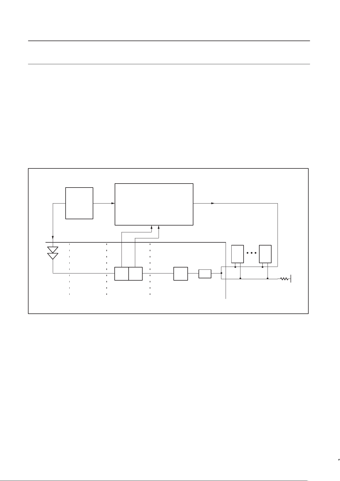
PCK2010
Direct Rambus
Clock Generator
(DRCG)
Gear Ratio-
Logic
/4
DLL
MN
BUSCLK
REFCLK
RMC
PCLK
SYNCLK
RAC
RDRAMs
CONTROLLER
SynClk/N
Pclk/M
SW00290
Figure 1. System Clock Architecture
The ASIC drives the output clocks, Pclk and SynClk/N from the
Gear Ratio Logic to the DRCG Phase Detector inputs. The routing
of the Pclk/M and SynClk/N signal traces must be matched in
impedance and propagation delay on the ASIC as well as on the
board. These signals are not part of the Rambus Channel and their
routing must be matched by board designers.
After comparing the phases of Pclk/M and SynClk/N, the DRCG
Phase Detector drives a phase aligner that adjusts the phase of
DRCG output clock, Busclk. Since the other elements in the
distributed loop have a fixed delay, adjusting Busclk adjusts the
phase of SynClk and thus the phase of SynClk/N.
In this manner, the distributed loop adjusts the phase of SynClk/N to
match that of Pclk/M, eliminating the phase error at the input of the
DRCG. When the clocks are aligned, data can be exchanged
directly from the Pclk domain to the SynClk domain.
The Gear Ratio Logic supports four clock ratios (2.0, 1.5, 1.33, and
1.0), where the ratio is defined as the ratio of Pclk/SynClk. Since
Busclk = 4*SynClk, this ratio also is equal to 4*Pclk/Busclk. Other
ratios could be used, depending on particular system
implementations.
Page 5

Philips Semiconductors Preliminary specification
PCK201 1Direct Rambus Clock Generator
1999 Jan 19
5
Power Management Modes
The DRCG device has three operating states: NORMAL, CLKSTOP
and POWERDOWN. In Normal mode, the clock source is on, and
the output is enabled. In CLKSTOP mode, the clock source is on,
but the output is disabled (STOPB deasserted). In Powerdown
mode, the device is powered down with the control signal PwrDnB
equal to 0. The control signals Mult0, Mult1, S0, S1 and S2 must be
stable before power is applied to the device, and can only be
changed in Power-down mode (PWRDNB=0).
T able 2. POWER MANAGEMENT MODES
MODE PwrDnB StopB Clk ClkB
NORMAL 1 1 PACLK PACLKB
CLKSTOP 1 0 VX, STOP VX, STOP
POWERDOWN 0 X GND GND
Upon applying power to the device, the device can enter any state,
depending on the settings of the control signals, PwrDnB and StopB.
The clock source output need not be glitch-free during state
transitions.
SW00360
DRCG
B
A
PPL
X
PWRDNB S0 S1 S2 STOPB
CLK
CLKB
PACLK
PHASE
ALIGNER
ΦD
SYNCLKNPCLKM
2
MULT
0
MULT
1
REFCLK
PLLCLK
TEST MUX
BYPASS MUX
BYPCLK
Figure 2. Direct Rambus Clock Generator Package
Page 6

Philips Semiconductors Preliminary specification
PCK201 1Direct Rambus Clock Generator
1999 Jan 19
6
Pclk
SynClk
Pclk/M =
SynClk/N
SW00292
Figure 3. Gear Ratio Timing Diagram
PHYSICAL SPECIFICATION
General Requirements
The clock source generates differential signals with specified jitter,
voltage levels, duty cycle, and rise/fall times. Figure 5 shows the
clock equivalent circuit.
SW00291
Differential
Driver
CHANNEL
R
T
= Z
CH
RT = Z
CH
Z
CH
Z
CH
Figure 4. Equivalent Circuit
The driver produces a specified voltage swing on the Channel. The
nominal value of the Channel impedance, Z CH , is 28 ohms.
In order to reduce signal attenuation and EMI, clock signal rise/fall
times are controlled to within specifications. In addition, DRCG is
able to receive input signals that are generated from different
voltage power supplies. The phase detector signals come from the
controller. The controller output voltage supply is connected to the
pin VddIPD of DRCG, and is used as the reference for the
two-phase detector input signals, PclkM and SynClkN. The output
voltage supply is also used as the reference for the output
enable/disable signal, StopB.
The reference clock comes from the main clock source chip. The
main clock source output voltage supply is connected to the pin
VddIR of DRCG, and is used as the reference for the Refclk input
signal.
Clock Jitter
The short-term jitter specification (over four cycles) for the clock
source is under 100 ps maximum. Jitter is measured using a jitter
measurement system that provides flexibility for measuring
cycle-cycle jitter as a function of cycle count.
Clock Source Specification
Rambus clock sources meet the output specifications listed in
Table 4 when characterized under the operating conditions listed in
Table 3.
Page 7

Philips Semiconductors Preliminary specification
PCK201 1Direct Rambus Clock Generator
1999 Jan 19
7
T able 3. DC DEVICE CHARACTERISTICS
Symbol Parameter Min Max Unit
V DD Supply voltage 3.135 3.465 V
T A Ambient operating temperature 0 70 °C
t
CYCLE ,IN
Refclk Input cycle time 10 40 ns
t
J,IN
Input Cycle-to-cycle jitter
1
– 250 ps
DC
IN
Input duty cycle over 10,000 cycles 40% 60% t
CYCLE
f
M,IN
3
Input frequency of modulation 30 33 kHz
P
M,IN
Modulation index 0.25 0.5 %
Modulation index for triangular modulation – 0.6
P
M,IN
3
Modulation index for non-triangular modulation
4
– 0.5
4
%
t
CYCLE,PD
Phase Detector input cycle time at PclkM & SynClkN 30 100 ns
t
ERR,INIT
Initial Phase error at Phase Detector inputs (Required range of Phase Aligner) –0.5 0.5 t
CYCLE,PD
DC
IN,PD
Phase Detector input duty cycle over 10,000 cycles 25% 75% t
CYCLE,PD
t
IR
, t
IF
Input slew rate (measured at 20% – 80% of input voltage) for PclkM, SynClkN, and Refclk 1 4 V/ns
C
IN,PD
Input capacitance at PclkM, SynClkN, and Refclk
2
– 7 pF
∆C
IN,PD
Input capacitance matching at PclkM and SynClkN
2
– 0.5 pF
C
IN,CMOS
Input capacitance at CMOS pins
2
– 10 pF
V
IL
Input (CMOS) signal low voltage – 0.3 Vdd
V
IH
Input (CMOS) signal high voltage 0.7 – Vdd
V
IL,R
Refclk input low voltage – 0.3 VddI,R
V
IH,R
Refclk input high voltage 0.7 – VddI,R
V
IL,PD
Input signal low voltage for PD inputs and StopB – 0.3 VddI,PD
V
IH,PD
Input signal high voltage for PD inputs and StopB 0.7 – VddI,PD
V
DDI,R
Input supply reference for Refclk 1.3 3.3 V
V
DDI,PD
Input supply reference for PD inputs 1.3 3.3 V
NOTES:
1. Refclk jitter measured at V
DDI,R
(nom)/2
2. Capacitance measured at Freq = 1MHz, DC bias = 0.9V, and V
AC
< 100mV
3. If the input modulation is used, input modulation is allowed but not required.
4. The amount of allowed spreading for any non-triangular modulation is determined by the induced downstream tracking skew, which cannot
exceed the skew generated by the specified 0.6% triangular modulation. Typically, the amount of allowed non-triangular modulation is about
0.5%.
Page 8

Philips Semiconductors Preliminary specification
PCK201 1Direct Rambus Clock Generator
1999 Jan 19
8
T able 4. AC DEVICE CHARACTERISTICS
Symbol Parameter Min Max Unit
t
CYCLE
Clock cycle time 2.5 3.75 ns
Cycle-to-cycle jitter at Clk/ClkB – 60 ps
t
J
Total jitter over 2, 3, or 4 clock cycles
1
– 100 ps
t
STEP
Phase Aligner phase step size (at Clk/ClkB) 1 – ps
t
ERR,PD
Phase Detector phase error for distributed loop Measured at PclkM-SynClkN (rising edges) (does not
include clock jitter)
– 100 100 ps
t
ERR,SSC
PLL output Phase error when tracking SSC – 100 100 ps
DC Output duty cycle over 10,000 cycles 40% 60% t
CYCLE
t
DC,ERR
Output cycle-to-cycle duty cycle error – 50 ps
t
CR
, t
CF
Output rise and fall times (measured at 20% – 80% of output voltage) 250 500 ps
t
CR,CF
Difference between rise and fall times on a single device (20% – 80%) – 100 ps
VX, stop Output voltage during Clkstop (StopB = 0) 1.1 2.0 V
V
X
Differential output crossing-point voltage 1.3 1.8 V
V
COS
Output voltage swing (p-p single-ended) 0.4 0.6 V
V
OH
Output HIGH voltage – 2.0 V
V
OL
Output LOW voltage 1.0 – V
R
OUT
Output dynamic resistance (at pins) 12 50 Ω
I
OZ
Output current during Hi-Z (S0 = 0, S1 = 1) – 50 µA
IOZ, stop Output current during ClkStop (StopB = 0) – 500 µA
I
powerdown
Current on powerdown (PwrDnB = 0) – 200 µA
I
ClkStop
Current on ClkStop (StopB = 0) 50 mA
I
normal
Current on normal state (StopB = 1) 100 mA
NOTE:
1. Output jitter specs measured at t
CYCLE
= 2.5ns.
2. V
COS
= VOH – V
OL
3. R
out
= ∆VO/∆IO; this is defined at the output pins.
T able 5. DRCG FUNCTIONS
REFCLK MULT0 MULT1 PLL CLK/CLKB MODE S0 S1 S2 CLK CLKB
pin2 pin15 pin14 multiplier pins 20/18 pin 24 pin 23 pin 13 pin 20 pin 18
33 1 1 8 267 Normal 0 0 0 PAclk PAclk
50 0 1 6 300 Bypass 1 0 0 PLLclk PLLclk
50 1 1 8 400 Test 1 1 0 Refclk Refclk
67 0 0 4 267 Vendor Test A 0 0 1 – –
67 0 1 6 400 Vendor Test B 1 0 1 – –
100 1 0 8/3 267 Reserved 1 1 1 – –
Output Test 0 1 x Hi-Z Hi-Z
Page 9

Philips Semiconductors Preliminary specification
PCK201 1Direct RAMbus Clock Generator
1999 Jan 19
9
SSOP24: plastic shrink small outline package; 24 leads; body width 5.3 mm SOT340-1
Page 10

Philips Semiconductors Preliminary specification
PCK201 1Direct RAMbus Clock Generator
1999 Jan 19
10
NOTES
Page 11

Philips Semiconductors Preliminary specification
PCK201 1Direct RAMbus Clock Generator
yyyy mmm dd
11
Definitions
Short-form specification — The data in a short-form specification is extracted from a full data sheet with the same type number and title. For
detailed information see the relevant data sheet or data handbook.
Limiting values definition — Limiting values given are in accordance with the Absolute Maximum Rating System (IEC 134). Stress above one
or more of the limiting values may cause permanent damage to the device. These are stress ratings only and operation of the device at these or
at any other conditions above those given in the Characteristics sections of the specification is not implied. Exposure to limiting values for extended
periods may affect device reliability.
Application information — Applications that are described herein for any of these products are for illustrative purposes only. Philips
Semiconductors make no representation or warranty that such applications will be suitable for the specified use without further testing or
modification.
Disclaimers
Life support — These products are not designed for use in life support appliances, devices or systems where malfunction of these products can
reasonably be expected to result in personal injury . Philips Semiconductors customers using or selling these products for use in such applications
do so at their own risk and agree to fully indemnify Philips Semiconductors for any damages resulting from such application.
Right to make changes — Philips Semiconductors reserves the right to make changes, without notice, in the products, including circuits, standard
cells, and/or software, described or contained herein in order to improve design and/or performance. Philips Semiconductors assumes no
responsibility or liability for the use of any of these products, conveys no license or title under any patent, copyright, or mask work right to these
products, and makes no representations or warranties that these products are free from patent, copyright, or mask work right infringement, unless
otherwise specified.
Philips Semiconductors
811 East Arques Avenue
P.O. Box 3409
Sunnyvale, California 94088–3409
Telephone 800-234-7381
Copyright Philips Electronics North America Corporation 1998
All rights reserved. Printed in U.S.A.
print code Date of release: 05-96
Document order number: 9397-750-04956
Data sheet
status
Objective
specification
Preliminary
specification
Product
specification
Product
status
Development
Qualification
Production
Definition
[1]
This data sheet contains the design target or goal specifications for product development.
Specification may change in any manner without notice.
This data sheet contains preliminary data, and supplementary data will be published at a later date.
Philips Semiconductors reserves the right to make chages at any time without notice in order to
improve design and supply the best possible product.
This data sheet contains final specifications. Philips Semiconductors reserves the right to make
changes at any time without notice in order to improve design and supply the best possible product.
Data sheet status
[1] Please consult the most recently issued datasheet before initiating or completing a design.
 Loading...