

Page 1

INTEGRATED CIRCUITS
PCK2010R
CK98R (100/133MHz) RCC spread
spectrum system clock generator
Product specification 1999 Oct 19
Page 2
Philips Semiconductors Product specification
CK98R (100/133MHz) RCC spread spectrum
system clock generator
FEA TURES
•Mixed 2.5 V and 3.3 V operation
•Four CPU clocks at 2.5 V
•Eight PCI clocks at 3.3 V, one free-running
(synchronous with CPU clocks)
•Four 3.3 V fixed clocks @ 66 MHz
•Two 2.5 V CPUDIV2 clocks @ ½ CPU clock frequency
•Three 2.5 V IOAPIC clocks @ 16.67 MHz
•One 3.3 V 48 MHz USB clock
•Two 3.3 V reference clocks @ 14.318 MHz
•Reference 14.31818 MHz Xtal oscillator input
•133 MHz or 100 MHz operation
•Power management control input pins
•CPU clock jitter ≤ 250 ps cycle-cycle
•CPU clock skew ≤ 175 ps pin-pin
•0.0ns – 1.5 ns CPU - 3V66 delay
•1.5ns – 3.5 ns 3V66 - PCI delay
•1.5ns – 4.0 ns CPU - IOAPIC delay
•1.5ns – 4.0 ns CPU - PCI delay
•Available in 56-pin SSOP package
•±0.5% center spread spectrum capability via select pins
•–0.5% down spread spectrum capability via select pins
DESCRIPTION
The PCK2010R is a clock generator (frequency synthesizer) chip for
a Pentium II and other similar processors.
The PCK2010R has four CPU clock outputs at 2.5 V, two CPUDIV2
clock outputs running at ½ CPU clock frequency (66 MHz or 50 MHz
depending on the state of SEL133/100) and four 3V66 clocks
running at 66MHz. There are eight PCI clock outputs running at
33 MHz. One of the PCI clock outputs is free-running. Additionally,
the part has three 2.5 V IOAPIC clock outputs at 16.67 MHz and two
3.3 V reference clock outputs at 14.318 MHz. All clock outputs meet
Intel’s drive strength, rise/fall time, jitter , accuracy, and skew
requirements.
The part possesses dedicated power-down, CPUSTOP
PCISTOP
input pins for power management control. These inputs
are synchronized on-chip and ensure glitch-free output transitions.
When the CPUSTOP input is asserted, the CPU clock outputs and
3V66 clock outputs are driven LOW. When the PCISTOP
asserted, the PCI clock outputs are driven LOW.
, and
input is
Finally, when the PWRDWN input pin is asserted, the internal
reference oscillator and PLLs are shut down, and all outputs are
driven LOW.
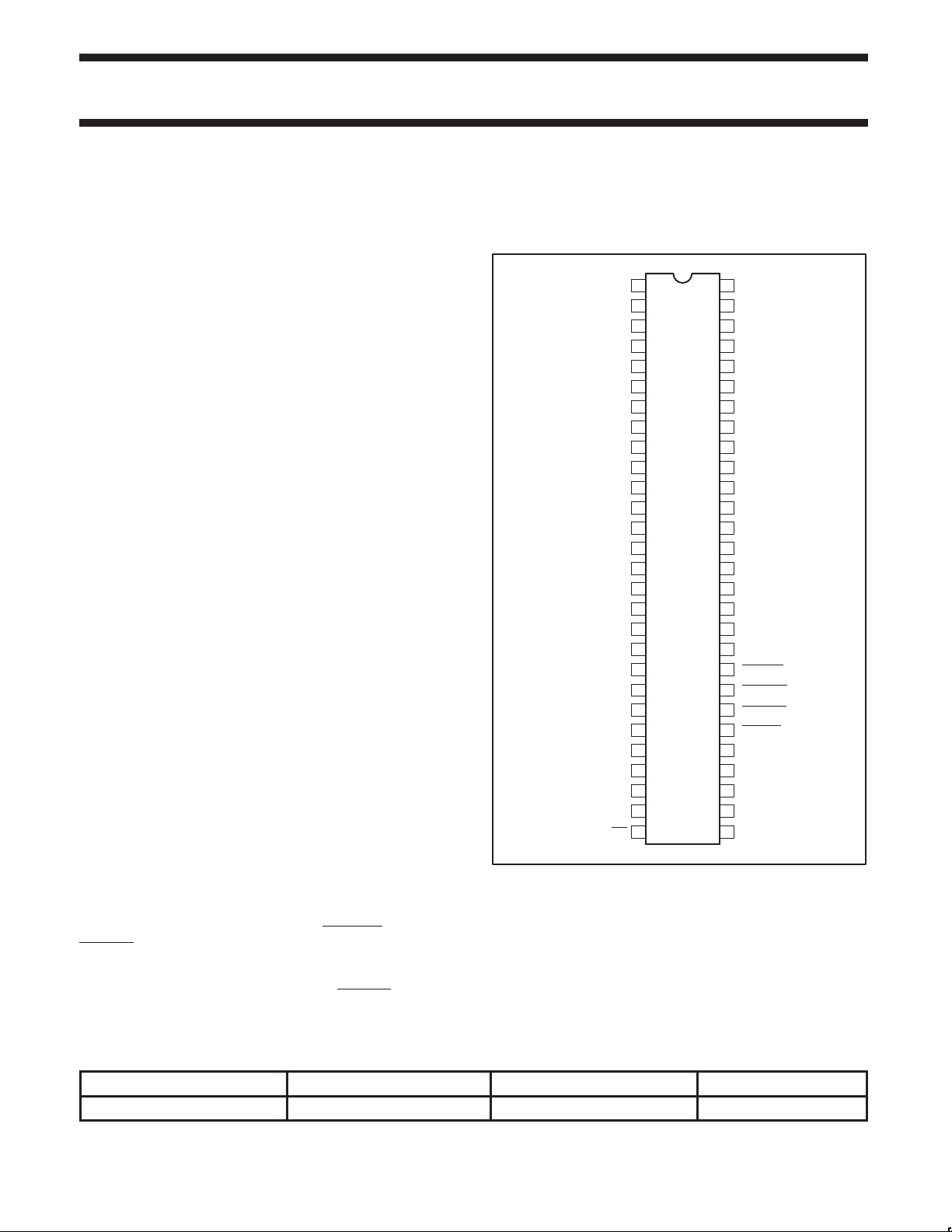
PIN CONFIGURATION
REF0
REF1
V
DD
XTAL_IN
XTAL_OUT
V
PCICLK_F
PCICLK1
V
DD
PCICLK2
PCICLK3
PCICLK4
PCICLK5
VDD3V
PCICLK6
PCICLK7
V
3V66_0
3V66_1
VDD3V
V
3V66_0
3V66_1
VDD3V
1
SS
2
3
4
3V
5
6
7
SS
8
9
10
3V
11
12 45
13
SS
14
15
16
17
18 39
19 38V
SS
20
SS
21
22
23
24
SS
25 32
26 31
27 30
28 29SEl133/100
PCK2010R
56V
V
25V
DD
55
APIC2
54
APIC1
APIC0
53
52
V
SS
51
25V
V
DD
50
CPUDIV2_1
CPUDIV2_0
49
48
V
SS
VDD25V
47
CPUCLK3
46
CPUCLK2
V
44V
SS
VDD25V
43
CPUCLK1
42
CPUCLK0
41
V
40
SS
3V
V
DD
V
SS
PCISTOP
37
CPUSTOP
36
35
PWRDWN
SPREAD
34
SEL1
33
SEL0
VDD3V
48MHz_USB
V
SS
SW00504
ORDERING INFORMA TION
PACKAGES TEMPERATURE RANGE ORDER CODE DRAWING NUMBER
56-Pin plastic SSOP 0°C to +70°C PCK2010R DL SOT371-1
Intel and Pentium are registered trademarks of Intel Corporation.
1999 Oct 19 853–2179 22543
2
Page 3
Philips Semiconductors Product specification
CK98R (100/133MHz) RCC spread spectrum
PCK2010R
system clock generator
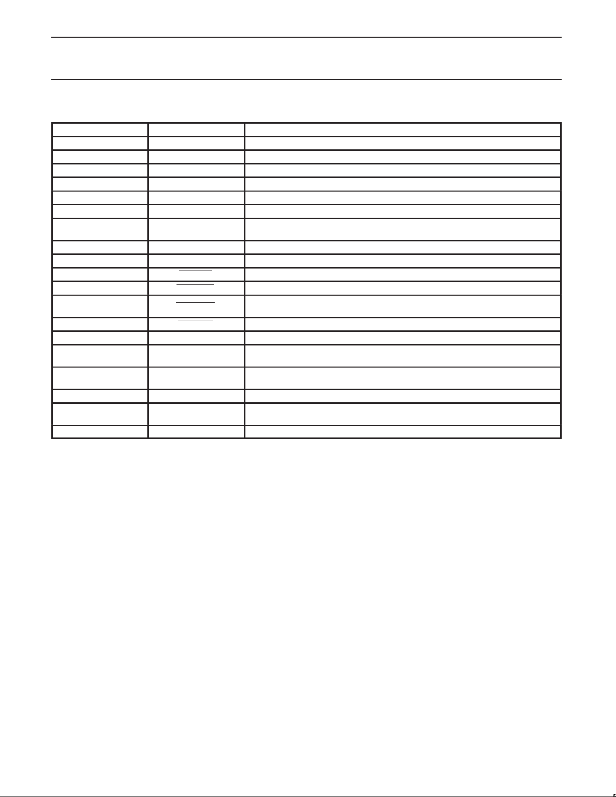
PIN DESCRIPTION
PIN NUMBER SYMBOL FUNCTION
2,3 REF [0–1] 3.3 V 14.318 MHz clock output
5 XTAL_IN 14.318 MHz crystal input
6 XTAL_OUT 14.318 MHz crystal output
8 PCICLK_F 3.3 V free running PCI clock
9, 11, 12, 14, 15, 17, 18 PCICLK [1–7] 3.3 V PCI clock outputs
21, 22, 25, 26 3V66 [0–3] 3.3 V fixed 66 MHz clock outputs
28 SEL133/100
30 48 MHz USB 3.3 V fixed 48 MHZ clock output
32, 33 SEL [0–1] Logic select pins. TTL levels.
34 SPREAD 3.3 V LVTTL input. Enables spread spectrum mode when held LOW.
35 PWRDWN 3.3 V LVTTL input. Device enters powerdown mode when held LOW.
36 CPUST OP
37 PCISTOP 3.3 V LVTTL input. Stops all PCI clocks except PCICLK_F when held LOW.
41, 42, 45, 46 CPUCLK [0–3] 2.5 V CPU output. 133 MHz or 100MHz depending on state of input pin SEL133/100.
49, 50 CPUDIV_2 [0–1]
53, 54, 55 IOAPIC [0–2]
4, 10, 16, 23, 27, 31, 39 V
1, 7, 13, 19, 20, 24, 29,
38, 40, 44, 48, 52
43, 47, 51, 56 V
NOTE:
1. V
, V
DD3V
on the performance of the device. In reality, the platform will be configured with the V
tied to a common 3.3 V supply and all V
and VSS in the above tables reflects a likely internal POWER and GROUND partition to reduce the effects of internal noise
DD25V
DD3V
V
SS
DD25V
pins being common.
SS
Select input pin for enabling 133 MHz or 100 MHz CPU outputs.
H = 133 MHz, L = 100 MHz
3.3 V LVTTL input. Stops all CPU clocks and 3V66 clocks when held LOW. CPUDIV_2
output remains on all the time.
2.5 V output running at 1/2 CPU clock frequency. 66 MHz or 50 MHz depending on
state of input pin SEL133/100.
2.5 V clock outputs running divide synchronous with the CPU clock frequency. Fixed
16.67 MHz limit.
3.3 V power supply.
Ground
2.5 V power supply
pins tied to a 2.5 V supply, all remaining V
DD25V
DD
pins
1999 Oct 19
3
Page 4
Philips Semiconductors Product specification
CK98R (100/133MHz) RCC spread spectrum
system clock generator
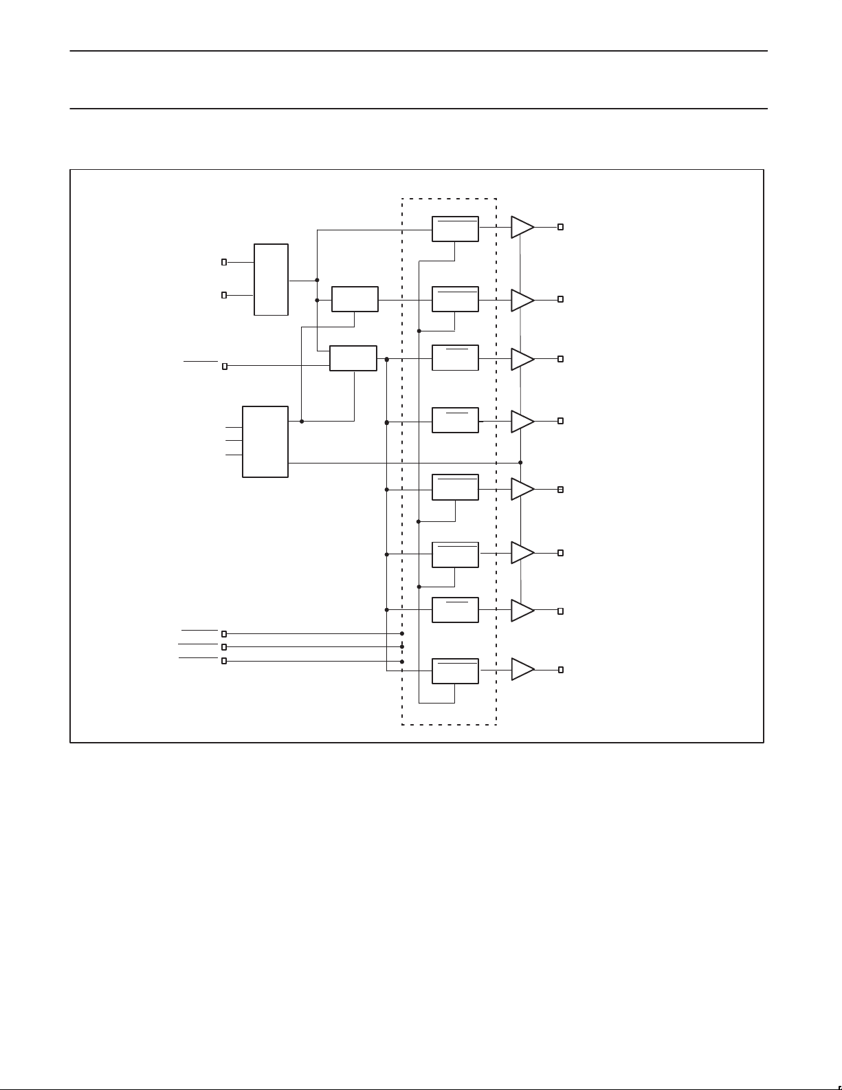
BLOCK DIAGRAM
XTAL_IN
X
14.318
MHZ
XTAL_OUT
SPREAD
SEL133/100
SEL0
SEL1
OSC
X
X
DECODE
LOGIC
USBPLL
SYSPLL
LOGIC
PWRDWN
LOGIC
PWRDWN
LOGIC
STOP
LOGIC
STOP
LOGIC
REF [0–1](14.318 MHz)
X
X
48 MHz USB
CPUCLK [0–3]
X
3V66 [0–3] (66MHz)
X
PCK2010R
PCISTOP
CPUSTOP
PWRDWN
PWRDWN
LOGIC
PWRDWN
LOGIC
STOP
LOGIC
X
X
X
PWRDWN
LOGIC
CPUDIV2 [0–1]
X
PCICLK_F (33MHz)
X
PCICLK [1–7] (33 MHz)
X
APIC [0–2] (16.67 MHz)
X
SW00505
1999 Oct 19
4
Page 5
Philips Semiconductors Product specification
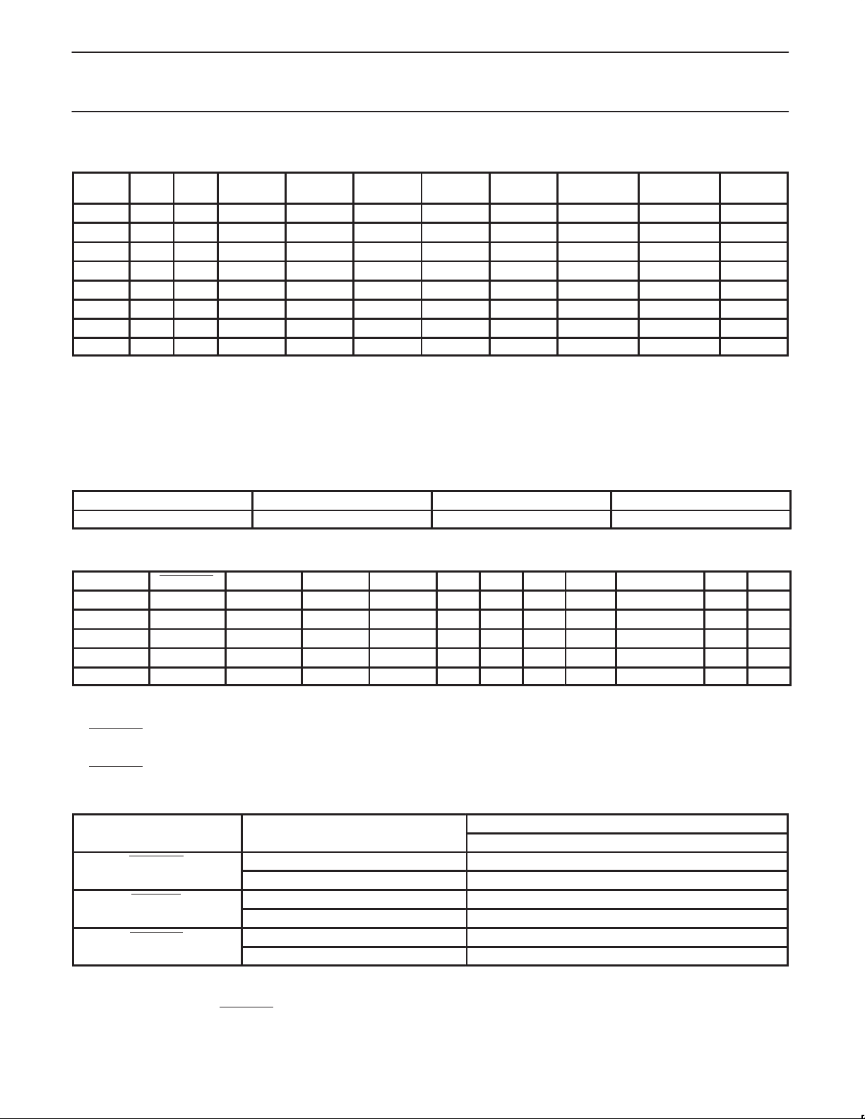
SIGNAL
SIGNAL STATE
CK98R (100/133MHz) RCC spread spectrum
PCK2010R
system clock generator
FUNCTION TABLE
SEL
133/100
NOTES:
1. Required for board level “bed-of-nails” testing.
2. Used to support Intel confidential application.
3. 48 MHz PLL disabled to reduce component jitter. 48 MHz outputs to be held Hi-Z instead of driven to LOW state.
4. “Normal” mode of operation.
5. TCLK is a test clock over driven on the XTALIN input during test mode. TCLK mode is based on 133 MHz CPU select logic.
6. Required for DC output impedance verification.
7. Frequency accuracy of 48 MHz must be +167 PPM to match USB default.
8. Range of reference frequency allowed is MIN = 14.316 MHz, NOMINAL = 14.31818 MHz, MAX = 14.32 MHz
SEL1 SEL0 CPU CPUDIV2 3V66 PCI 48 MHz REF IOAPIC NOTES
0 0 0 HI-Z HI-Z HI-Z HI-Z HI-Z HI-Z HI-Z 1
0 0 1 N/A N/A N/A N/A N/A N/A N/A 2
0 1 0 100 MHz 50 MHz 66 MHz 33 MHz HI-Z 14.318 MHz 16.67 MHz 3
0 1 1 100 MHz 50 MHz 66 MHz 33 MHz 48 MHz 14.318 MHz 16.67 MHz 4, 7, 8
1 0 0 TCLK/2 TCLK/4 TCLK/4 TCLK/8 TCLK/2 TCLK TCLK/16 5, 6
1 0 1 N/A N/A N/A N/A N/A N/A N/A 2
1 1 0 133 MHz 66 MHz 66 MHz 33 MHz HI-Z 14.318 MHz 16.67 MHz 3
1 1 1 133 MHz 66 MHz 66 MHz 33 MHz 48 MHz 14.318 MHz 16.67 MHz 4, 7, 8
CLOCK OUTPUT
USBCLK
7
TARGET FREQUENCY (MHz) ACTUAL FREQUENCY (MHz) PPM
48.0 48.008 167
CLOCK ENABLE CONFIGURATION
CPUSTOP PWRDWN PCISTOP CPUCLK CPUDIV2 APIC 3V66 PCI PCI_F REF / 48 MHz OSC VCOs
X 0 X LOW LOW LOW LOW LOW LOW LOW OFF OFF
0 1 0 LOW ON ON LOW LOW ON ON ON ON
0 1 1 LOW ON ON LOW ON ON ON ON ON
1 1 0 ON ON ON ON LOW ON ON ON ON
1 1 1 ON ON ON ON ON ON ON ON ON
NOTES:
1. LOW means outputs held static LOW as per latency requirement below
2. ON means active.
3. PWRDWN
4. All 3V66 clocks as well as CPU clocks should stop cleanly when CPUSTOP is pulled LOW.
5. CPUDIV2, IOAPIC, REF, 48 MHz signals are not controlled by the CPUSTOP functionality and are enabled all in all conditions except when
PWRDWN
pulled LOW, impacts all outputs including REF and 48 MHz outputs.
is LOW.
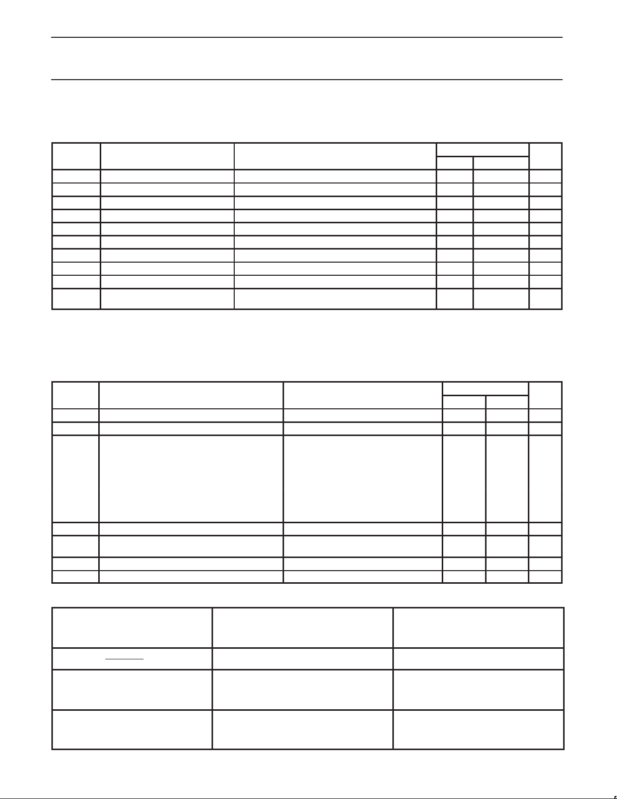
POWER MANAGEMENT REQUIREMENTS
LATENCY
NO. OF RISING EDGES OF FREE RUNNING PCICLK
CPUSTOP
PCISTOP
PWRDWN
NOTES:
1. Clock ON/OFF latency is defined as the number of rising edges of free running PCICLKs between the clock disable goes HIGH/LOW to the
first valid clock that comes out of the device.
2. Power up latency is when PWRDWN
goes inactive (HIGH) to when the first valid clocks are driven from the device.
0 (DISABLED) 1
1 (ENABLED) 1
0 (DISABLED) 1
1 (ENABLED) 1
1 (NORMAL OPERATION) 3 ms
0 (POWER DOWN) 2 MAX
1999 Oct 19
5
Page 6
Philips Semiconductors Product specification
SYMBOL
PARAMETER
CONDITION
UNIT
SYMBOL
PARAMETER
CONDITIONS
UNIT
C
CK98R (100/133MHz) RCC spread spectrum
PCK2010R
system clock generator
ABSOLUTE MAXIMUM RATINGS
In accordance with the Absolute Maximum Rating System (IEC 134)
Voltages are referenced to VSS (VSS = 0 V)
V
DD3
V
DDQ3
V
DDQ2
I
IK
V
I
OK
V
O
I
O
T
STG
P
TOT
NOTES:
1. Stresses beyond those listed may cause permanent damage to the device. These are stress ratings only and functional operation of the
device at these or any other conditions beyond those indicated under “recommended operating conditions” is not implied. Exposure to
absolute-maximum-rated conditions for extended periods may affect device reliability .
2. The input and output voltage ratings may be exceeded if the input and output current ratings are observed.
DC 3.3 V core supply voltage –0.5 +4.6 V
DC 3.3 V I/O supply voltage –0.5 +4.6 V
DC 2.5 V I/O supply voltage –0.5 +3.6 V
DC input diode current VI < 0 –50 mA
DC input voltage Note 2 –0.5 5.5 V
I
DC output diode current VO > VCC or VO < 0 ±50 mA
DC output voltage Note 2 –0.5 VCC + 0.5 V
DC output source or sink current VO = 0 to V
Storage temperature range –65 +150 °C
Power dissipation per package
plastic medium-shrink (SSOP)
1, 2
CC
For temperature range: –40 to +125°C
above +55°C derate linearly with 11.3mW/K
LIMITS
MIN MAX
±50 mA
850 mW
RECOMMENDED OPERATING CONDITIONS
V
DD3V
V
DD25V
V
f
REF
T
V
amb
DC 3.3 V core supply voltage 3.135 3.465 V
DC 2.5 V I/O supply voltage 2.375 2.625 V
Capacitive load on:
CPUCLK 1 device load, possible 2 loads 10 20 pF
PCICLK Must meet PCI 2.1 requirements 10 30 pF
L
CPUDIV2 1 device load, possible 2 loads 10 20 pF
3V66 1 device load, possible 2 loads 10 30 pF
48 MHz clock USB 1 device load 10 20 pF
REF 1 device load 10 20 pF
IOAPIC 1 device load 10 20 pF
DC input voltage range 0 V
I
DC output voltage range 0
O
Reference frequency, oscillator nominal value 14.31818 14.31818 MHz
Operating ambient temperature range in free air 0 +70 °C
POWER MANAGEMENT
MAXIMUM 2.5V SUPPLY CONSUMPTION
CK133
CONDITION
Power-down mode
(PWRDWN = 0)
Full active 100 MHz
SEL133/100# = 0
SEL1, 0 = 1 1
CPUSTOP, PCISTOP = 1
Full active 133 MHz
SEL133/100# = 1
SEL1, 0 = 1 1
CPUSTOP, PCISTOP = 1
MAXIMUM DISCRETE CAP LOADS,
ALL STATIC INPUTS = V
MAXIMUM 3.3V SUPPL Y CONSUMPTION
MAXIMUM DISCRETE CAP LOADS,
V
= 2.625 V
DD25V
DD3V
OR V
SS
ALL STATIC INPUTS = V
100 µA 200 µA
80 mA 160 mA
90 mA 160 mA
LIMITS
MIN MAX
V
= 3.465 V
DD25V
V
DD25V
V
DD3V
DD3V
DD3V
OR V
V
V
SS
1999 Oct 19
6
Page 7

Philips Semiconductors Product specification
TEST CONDITIONS
SYMBOL
PARAMETER
I
mA
I
,
mA
I
,
mA
I
mA
I
,
mA
I
,
mA
CK98R (100/133MHz) RCC spread spectrum
PCK2010R
system clock generator
DC CHARACTERISTICS
LIMITS
T
= 0°C to +70°C UNIT
amb
V
DD
(V)
V
V
V
V
V
V
±I
V
V
OH2
OL2
OH3
OL3
OH3
OL3
OH
OH
OH
OL
OL
OL
±I
IH
IL
I
OZ
HIGH level input voltage 3.135 to 3.465
LOW level input voltage 3.135 to 3.465
2.5 V output HIGH voltage
CPUCLK, IOAPIC, CPUDIV2
2.5 V output LOW voltage
CPUCLK, IOAPIC, CPUDIV2
3.3 V output HIGH voltage
REF, 48 MHz USB
3.3 V output LOW voltage
REF, 48 MHz USB
3.3 V output HIGH voltage
PCI, 3V66
3.3 V output LOW voltage
PCI, 3V66
CPUCLK
output HIGH current
48 MHz USB, REF
output HIGH current
PCI, 3V66
output HIGH current
CPUCLK
output LOW current
48 MHz USB, REF
output LOW current
PCI, 3V66
output LOW current
2.375 to 2.625 IOH = –1 mA 2.0 – V
2.375 to 2.625 IOL = 1 mA – 0.4 V
3.135 to 3.465 IOH = –1 mA 2.0 – V
3.135 to 3.465 IOL = 1 mA – 0.4 V
3.135 to 3.465 IOH = –1 mA 2.4 – V
3.135 to 3.465 IOL= 1 mA – 0.55 V
2.375 V
2.625 V
3.135 V
3.465 V
3.135 V
3.465 V
2.375 V
2.625 V
3.135 V
3.465 V
3.135 V
3.465 V
OUT
= 2.375 V – –27
OUT
OUT
= 3.135 V – –23
OUT
OUT
= 3.135 V – –33
OUT
OUT
OUT
OUT
OUT
OUT
OUT
Input leakage current 3.465 – 5 µA
3-State output OFF-State
current
3.465
V
OUT
Vdd or GND
Cin Input pin capacitance 5 pF
Cxtal
Xtal pin capacitance, as seen
by external crystal
Cout Output pin capacitance 6 pF
OTHER MIN TYP MAX
V
=
DD25V
2.5 V ±5%
V
=
DD3V
3.3 V ±5%
= 1.0 V –27 –
= 1.0 V –29 –
= 1.0 V –33 –
= 1.2 V 27 –
= 0.3 V – 30
2.0 VDD + 0.3 V
VSS – 0.3 0.8 V
= 1.95 V 29 –
= 0.4 V – 27
= 1.95 V 30 –
= 0.4 V – 38
=
IO = 0 – 10 µA
18 pF
1999 Oct 19
7
Page 8

Philips Semiconductors Product specification
CK98R (100/133MHz) RCC spread spectrum
PCK2010R
system clock generator
AC CHARACTERISTICS
V
= 3.3 V ± 5%; VDDAPIC = V
DD3V
CPU CLOCK OUTPUTS, CPU(0–3) (LUMP CAPACITANCE TEST LOAD = 20 pF)
SYMBOL PARAMETER
T
HKP
T
HKH
T
HKL
T
HRISE
T
HFALL
T
JITTER
DUTY CYCLE Output Duty Cycle 45 55 45 55 % 1
T
HSKW
CPUCLK period 7.5 8.0 10.0 10.5 ns 2, 9
CPUCLK HIGH time 1.87 n/a 3.0 n/a ns 5, 10
CPUCLK LOW time 1.67 n/a 2.8 n/a ns 6, 10
CPUCLK rise time 0.4 1.6 0.4 1.6 ns 8
CPUCLK fall time 0.4 1.6 0.4 1.6 ns 8
CPUCLK cycle-cycle jitter 250 250 ps
CPUCLK pin-pin skew 175 175 ps 2
= 2.5 V ± 5%; f
DD25V
= 14.31818 MHz
crystal
LIMITS
T
= 0°C to +70°C
amb
T
amb
133 MHz MODE 100 MHz MODE
MIN MAX MIN MAX
LIMITS
= 0°C to +70°C
UNIT NOTES
CPUDIV2 CLOCK OUTPUTS, CPUDIV2 (0–1) (LUMP CAPACITANCE TEST LOAD = 20 pF)
LIMITS
T
= 0°C to +70°C
SYMBOL PARAMETER
amb
133 MHz MODE 100 MHz MODE
MIN MAX MIN MAX
T
T
T
T
HRISE
T
HFALL
T
JITTER
HKP
HKH
HKL
CPUDIV2 CLK period 15.0 16.0 20.0 21.0 ns 2, 9
CPUDIV2 CLK HIGH time 5.25 n/a 7.5 n/a ns 5, 10
CPUDIV2 CLK LOW time 5.05 n/a 7.3 n/a ns 6, 10
CPUDIV2 CLK rise time 0.4 1.6 0.4 1.6 ns 8
CPUDIV2 CLK fall time 0.4 1.6 0.4 1.6 ns 8
CPUDIV2 CLK cycle-cycle jitter 250 250 ps
DUTY CYCLE CPUDIV2 CLK Duty Cycle 45 55 45 55 % 1
T
HSKW
CPUDIV2 CLK pin-pin skew 175 175 ps 2
LIMITS
T
= 0°C to +70°C
amb
UNIT NOTES
PCI CLOCK OUTPUTS, PCI(0–7) (LUMP CAPACITANCE TEST LOAD = 30 pF)
LIMITS
T
= 0°C to +70°C
SYMBOL PARAMETER
amb
133 MHz MODE 100 MHz MODE
MIN MAX MIN MAX
T
T
T
T
HRISE
T
HFALL
T
JITTER
HKP
HKH
HKL
PCICLK period 30.0 n/a 30.0 n/a ns 2, 9
PCICLK HIGH time 12.0 n/a 12.0 n/a ns 5, 10
PCICLK LOW time 12.0 n/a 12.0 n/a ns 6, 10
PCICLK rise time 0.5 2.0 0.5 2.0 ns 8
PCICLK fall time 0.5 2.0 0.5 2.0 ns 8
PCICLK cycle-cycle jitter 500 500 ps
DUTY CYCLE PCICLK Duty Cycle 45 55 45 55 % 1
T
HSKW
PCICLK pin-pin skew 500 500 ps 2
LIMITS
T
= 0°C to +70°C
amb
UNIT NOTES
1999 Oct 19
8
Page 9

Philips Semiconductors Product specification
CK98R (100/133MHz) RCC spread spectrum
PCK2010R
system clock generator
APIC(0–1) CLOCK OUTPUT (LUMP CAPACITANCE TEST LOAD = 20 pF)
LIMITS
T
= 0°C to +70°C
SYMBOL PARAMETER
amb
133 MHz MODE 100 MHz MODE
MIN MAX MIN MAX
T
T
T
T
HRISE
T
HFALL
T
JITTER
HKP
HKH
HKL
IOAPIC CLK period 60.0 64.0 60.0 64.0 ns 2, 9
IOAPIC CLK HIGH time 25.5 n/a 25.5 n/a ns 5, 10
IOAPIC CLK LOW time 25.3 n/a 25.3 n/a ns 6, 10
IOAPIC CLK rise time 0.4 1.6 0.4 1.6 ns 8
IOAPIC CLK fall time 0.4 1.6 0.4 1.6 ns 8
IOAPIC CLK cycle-cycle jitter 500 500 ps
DUTY CYCLE IOAPIC CLK Duty Cycle 45 55 45 55 % 1
T
HSKW
IOAPIC CLK pin-pin skew 250 250 ps 2
3V66 CLOCK OUTPUT, 3V66 (0–3) (LUMP CAPACITANCE TEST LOAD = 30 pF)
LIMITS
T
= 0°C to +70°C
SYMBOL PARAMETER
T
T
T
T
HRISE
T
HFALL
T
JITTER
HKP
HKH
HKL
3V66 CLK period 15.0 16.0 15.0 16.0 ns 2, 9, 4
3V66 CLK HIGH time 5.25 n/a 5.25 n/a ns 5, 10
3V66 CLK LOW time 5.05 n/a 5.05 n/a ns 6, 10
3V66 CLK rise time 0.4 1.6 0.4 1.6 ns 8
3V66 CLK fall time 0.4 1.6 0.4 1.6 ns 8
3V66 CLK cycle-cycle jitter 500 500 ps
DUTY CYCLE 3V66 CLK Duty Cycle 45 55 45 55 % 1
T
HSKW
3V66 CLK pin-pin skew 250 250 ps 2
amb
133 MHz MODE 100 MHz MODE
MIN MAX MIN MAX
LIMITS
T
= 0°C to +70°C
amb
LIMITS
T
= 0°C to +70°C
amb
UNIT NOTES
UNIT NOTES
48MHZ(0–1) CLOCK OUTPUT (LUMP CAPACITANCE TEST LOAD = 20 pF)
SYMBOL PARAMETER
TEST CONDITIONS
NOTES MIN MAX
f Frequency, Actual
f
D
T
(tR) Output rise edge rate 1 4 ns
HRISE
T
(tF) Output fall edge rate 1 4 ns
HFALL
Deviation from 48 MHz (48.008 – 48)/48 +167 ppm
Determined by PLL
divider ratio
DUTY CYCLE (tD) Duty Cycle 45 55 %
133 MHz 100 MHz
T
JITTER
CLK cycle-cycle jitter
MIN MAX MIN MAX
500 500
T
(fST) Frequency stabilization from Power-up (cold start) 3 ms
HSTB
NOTE:
1. See Figure 5 for measure points.
1999 Oct 19
9
LIMITS
T
= 0°C to +70°C
amb
48.008 MHz
UNIT
ps
Page 10

Philips Semiconductors Product specification
TEST CONDITIONS
SYMBOL
PARAMETER
UNIT
NOTES
CK98R (100/133MHz) RCC spread spectrum
PCK2010R
system clock generator
AC CHARACTERISTICS (Continued)
LIMITS
T
= 0°C to +70°C
amb
Measurement loads
(lumped)
T
HPOFFSET
T
HPOFFSET
T
HPOFFSET
T
HPOFFSET
T
HPOFFSET
NOTES:
1. Output drivers must have monotonic rise/fall times through the specified V
2. Period, jitter, offset and skew measured on rising edge @1.25 V for 2.5 V clocks and @ 1.5 V for 3.3 V clocks.
3. The PCICLK is the CPUCLK divided by four at CPUCLK = 133 MHz. The 3V66 CLK is internal VCO frequency divided by three at
CPUCLK = 100 MHz.
4. 3V66 CLK is internal VCO frequency divided by two at CPUCLK = 133 MHz. The 3V66 CLK is internal VCO frequency divided by three at
CPUCLK = 100 MHz.
5. T
6. T
7. The time is specified from when V
8. T
9. The average period over any 1 µs period of time must be greater than the minimum specified period.
10.Calculated at minimum edge-rate (1V/ns) to guarantee 45/55% duty-cycle. Pulse width is required to be wider at faster edge-rate to ensure
11.Output (see Figure 5 for measure points).
is measured at 2.0 V for 2.5 V outputs, 2.4 V for 3.3 V outputs as shown in Figure 4.
HKH
is measured at 0.4 V for all outputs as shown in Figure 4.
HKL
stable and operating within specification.
and T
HRISE
duty-cycle specification is met.
CPUCLK to 3V66 CLK,
CPU leads
3V66 CLK to PCICLK,
3V66 leads
CPUCLK to IOAPIC,
CPU leads
CPUCLK to PCICLK ,
CPU leads
CPUDIV2 to CPUCLK,
CPUDIV2 leads
achieves its nominal operating level (typical condition V
DDQ
are measured as a transition through the threshold region VOL = 0.4 V and VOH = 2.4 V (1 mA) JEDEC specification.
HFALL
CPU@20 pF,
3V66@30 pF
3V66@30 pF,
PCI@30 pF
CPU@20 pF,
IOAPIC@20 pF
CPU@20 pF
PCI@30 pF
CPUDIV2@20 pF
CPU@20 pF
Measure points MIN TYP MAX
CPU@1.25 V ,
3V66@1.5 V
3V66@1.5 V ,
PCI@1.5 V
3CPU@1.25 V ,
IOAPIC@1.25 V
CPU@1.25 V
PCI@1.5 V
CPUDIV2@
CPU@1.25 V
levels.
OL/VOH
0.0 0.45 1.5 ns 1
1.5 2.0 3.5 ns 1
1.5 2.4 4.0 ns 1
1.5 3.8 4.0 ns
0.0 1.6 2.5 ns
= 3.3 V) until the frequency output is
DDQ
1999 Oct 19
10
Page 11

Philips Semiconductors Product specification
Function
48 MHz PLL
CK98R (100/133MHz) RCC spread spectrum
PCK2010R
system clock generator
SPREAD SPECTRUM FUNCTION TABLE
SPREAD# SEL133/100# SEL1 SEL0
pin 34 pin 28 pin 33 pin 32
0 (active) 0 (100 MHz) 0 0 3-State to High Impedance Inactive
0 (active) 0 (100 MHz) 0 1 100 MHz, Center Spread ±0.5% Active
0 (active) 0 (100 MHz) 1 0 100 MHz, Down Spread – 0.5% Inactive
0 (active) 0 (100 MHz) 1 1 100 MHz, Down Spread – 0.5% Active
0 (active) 1 (133 MHz) 0 0 Test Mode Active
0 (active) 1 (133 MHz) 0 1 133 MHz, Center Spread ±0.5% Active
0 (active) 1 (133 MHz) 1 0 133 MHz, Down Spread – 0.5% Inactive
0 (active) 1 (133 MHz) 1 1 133 MHz, Down Spread – 0.5% Active
1 (inactive) 0 (100 MHz) 0 0 3-State to High Impedance Inactive
1 (inactive) 0 (100 MHz) 0 1 100 MHz, No Center Spread ±0.5% Active
1 (inactive) 0 (100 MHz) 1 0 100 MHz, No Down Spread – 0.5% Inactive
1 (inactive) 0 (100 MHz) 1 1 100 MHz, No Down Spread – 0.5% Active
1 (inactive) 1 (133 MHz) 0 0 T est Mode Active
1 (inactive) 1 (133 MHz) 0 1 133 MHz, No Center Spread ±0.5% Active
1 (inactive) 1 (133 MHz) 1 0 133 MHz, No Down Spread – 0.5% Inactive
1 (inactive) 1 (133 MHz) 1 1 133 MHz, No Down Spread – 0.5% Active
1999 Oct 19
11
Page 12

Philips Semiconductors Product specification
CK98R (100/133MHz) RCC spread spectrum
system clock generator
AC WAVEFORMS
VM = 1.25 V @ V
VX = VOL + 0.3 V
VY = VOH –0.3 V
VOL and VOH are the typical output voltage drop that occur with the
output load.
and 1.5 V @ V
DDQ2
DDQ3
PCK2010R
1999 Oct 19
12
Page 13

Philips Semiconductors Product specification
CK98R (100/133MHz) RCC spread spectrum
system clock generator
V
DDQ2
CPUCLK
@133MHz
3v66
@66MHz
@ 66MHz
3V66
1.25V
1.5V
CPU leads 3V66
T
HPOFFSET
Figure 1. CPUCLK to 3V66 offset
1.5V
V
SS
V
DDQ3
V
SS
SW00354
V
DDQ3
V
SS
PCK2010R
PCICLK
@ 33MHz
CPUCLK
@ 133MHz
IOAPIC
@ 16.6MHz
1.5V
T
HPOFFSET
3V66 leads PCICLK
Figure 2. 3V66 to PCI offset
1.25V
1.25V
CPUCLK leads IOAPIC
T
HPOFFSET
Figure 3. CPU to IOAPIC offset
V
DDQ3
V
SS
SW00356
V
DDQ2
V
SS
V
DDQ2
V
SS
SW00357
1999 Oct 19
13
Page 14

Philips Semiconductors Product specification
CK98R (100/133MHz) RCC spread spectrum
system clock generator
T
HKP
DUTY CYCLE
T
HKH
2.5V CLOCKING
INTERFACE
3.3V CLOCKING
INTERFACE
(TTL)
COMPONENT
MEASUREMENT
POINTS
COMPONENT
MEASUREMENT
POINTS
Figure 5. Component versus system measure points
2.0
1.25
0.4
T
HKL
FALL
T
PKP
T
PKL
FALL
2.4
1.5
0.4
T
T
RISE
RISE
T
T
PKH
T
Figure 4. 2.5V/3.3V clock waveforms
V
OL
V
OL
2.5VOLT MEASURE POINTS
V
= 2.0V
OH
= 0.4V
V
SS
3.3VOLT MEASURE POINTS
VOH = 2.4V
= 0.4V
V
SS
V
DDQ2
= 1.7V
V
IH
1.25V
V
= 0.7V
IL
V
DDQ3
VIH = 2.0V
1.5V
VIL = 0.7V
SW00242
SYSTEM
MEASUREMENT
POINTS
SYSTEM
MEASUREMENT
POINTS
SW00243
PCK2010R
V
I
SEL133/100,
SEL1, SEL0
GND
V
DD
OUTPUT
LOW-to-OFF
OFF-to-LOW
V
OL
V
OH
OUTPUT
HIGH-to-OFF
OFF-to-HIGH
V
SS
1999 Oct 19
V
M
t
PLZ
outputs
enabled
t
PHZ
t
PZL
V
M
V
X
t
PZH
V
Y
outputs
disabled
V
M
outputs
enabled
SW00454
14
Page 15

Philips Semiconductors Product specification
CK98R (100/133MHz) RCC spread spectrum
system clock generator
Figure 6. 3-State enable and disable times
V
DD
V
PULSE
GENERATOR
I
R
T
D.U.T.
TEST S
t
PLH/tPHL
t
PLZ/tPZL
t
PHZ/tPZH
2<V
1
Open
V
SS
V
DD
PCK2010R
S
1
2<V
DD
Open
V
SS
O
C
L
500Ω
500Ω
PWRDWN
CPUCLK
(INTERNAL)
PCICLK
(INTERNAL)
PWRDWN
CPUCLK
(EXTERNAL)
PCICLK
(EXTERNAL)
OSC & VCO
VDD = V
DDQ2
or V
, DEPENDS ON THE OUTPUT
DDQ3
Figure 7. Load circuitry for switching times
SW00238
1999 Oct 19
USB (48MHz)
SW00244
Figure 8. Power Management
15
Page 16

Philips Semiconductors Product specification
CK98R (100/133MHz) RCC spread spectrum
PCK2010R
system clock generator
SSOP56: plastic shrink small outline package; 56 leads; body width 7.5 mm SOT371-1
1999 Oct 19
16
Page 17

Philips Semiconductors Product specification
CK98R (100/133MHz) RCC spread spectrum
system clock generator
NOTES
PCK2010R
1999 Oct 19
17
Page 18

Philips Semiconductors Product specification
CK98R (100/133MHz) RCC spread spectrum
system clock generator
Data sheet status
Data sheet
status
Objective
specification
Preliminary
specification
Product
specification
Product
status
Development
Qualification
Production
Definition
This data sheet contains the design target or goal specifications for product development.
Specification may change in any manner without notice.
This data sheet contains preliminary data, and supplementary data will be published at a later date.
Philips Semiconductors reserves the right to make changes at any time without notice in order to
improve design and supply the best possible product.
This data sheet contains final specifications. Philips Semiconductors reserves the right to make
changes at any time without notice in order to improve design and supply the best possible product.
[1]
PCK2010R
[1] Please consult the most recently issued datasheet before initiating or completing a design.
Definitions
Short-form specification — The data in a short-form specification is extracted from a full data sheet with the same type number and title. For
detailed information see the relevant data sheet or data handbook.
Limiting values definition — Limiting values given are in accordance with the Absolute Maximum Rating System (IEC 134). Stress above one
or more of the limiting values may cause permanent damage to the device. These are stress ratings only and operation of the device at these or
at any other conditions above those given in the Characteristics sections of the specification is not implied. Exposure to limiting values for extended
periods may affect device reliability.
Application information — Applications that are described herein for any of these products are for illustrative purposes only. Philips
Semiconductors make no representation or warranty that such applications will be suitable for the specified use without further testing or
modification.
Disclaimers
Life support — These products are not designed for use in life support appliances, devices or systems where malfunction of these products can
reasonably be expected to result in personal injury . Philips Semiconductors customers using or selling these products for use in such applications
do so at their own risk and agree to fully indemnify Philips Semiconductors for any damages resulting from such application.
Right to make changes — Philips Semiconductors reserves the right to make changes, without notice, in the products, including circuits, standard
cells, and/or software, described or contained herein in order to improve design and/or performance. Philips Semiconductors assumes no
responsibility or liability for the use of any of these products, conveys no license or title under any patent, copyright, or mask work right to these
products, and makes no representations or warranties that these products are free from patent, copyright, or mask work right infringement, unless
otherwise specified.
Philips Semiconductors
811 East Arques Avenue
P.O. Box 3409
Sunnyvale, California 94088–3409
Telephone 800-234-7381
Copyright Philips Electronics North America Corporation 1999
All rights reserved. Printed in U.S.A.
Date of release: 10-99
Document order number: 9397–750–06509
1999 Oct 19
18
 Loading...