

Page 1

INTEGRATED CIRCUITS
DATA SH EET
PCF8801
LCD driver for 140 × 2 segments
Product specification
File under Integrated Circuits, IC12
2000 Feb 04
Page 2

Philips Semiconductors Product specification
LCD driver for 140 × 2 segments PCF8801
FEATURES
• Single-chip LCD controller/driver
• Fixed backplane multiplexing at a rate of 1 : 2
• Internal LCD bias generation (0.5VDD)
• 140 segment outputs configured to drive seven
40-segment characters
• On-chip oscillator with one external resistor
• Wide power supply range (2.7 V up to 5.5 V)
• Low power consumption
• Compatible with most microprocessors/microcontrollers
• 1 MHz serial bus interface (280-bit shift register)
• Easily cascaded for large LCD applications (two
cascade directions possible)
• Compatible with chip-on-glass technology
• Manufactured by silicon gate CMOS process.
GENERAL DESCRIPTION
The PCF8801 is a peripheral device which interfaces a
multiplexed Liquid Crystal Display (LCD) having two
backplanes and up to 140 segments. It generates drive
signals at a multiplex rate of 1 : 2 allowing seven
40-segment (5 x 8) characters to be driven.
The chip can easily be cascaded for larger LCD
applications,andthedirectionoftheinformationflowinthe
cascadecanbeselected.ThePCF8801iscompatiblewith
most microprocessors/microcontrollers and
communicates via a serial bus interface comprising a
280-bit shift register.
Theoutputsaremultiplexedbyaclocksignalgeneratedby
the internal oscillator which needs only one external
resistor.Cascadeapplicationsonlyrequiretheclocksignal
to be generated by the first device with the internal
oscillators in the other devices disabled.
The PCF8801 is designed for chip-on-glass applications.
It has a narrow package with raised points (bumps) for
easy assembly on to LCD glass.
ORDERING INFORMATION
TYPE
NUMBER
PCF8801U − chip with bumps in tray −
NAME DESCRIPTION VERSION
PACKAGE
2000 Feb 04 2
Page 3
Philips Semiconductors Product specification
LCD driver for 140 × 2 segments PCF8801
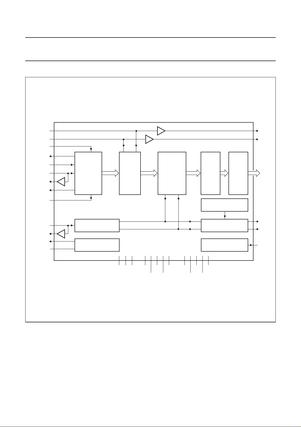
BLOCK DIAGRAM
handbook, full pagewidth
LDPI
LDNI
DI1
DO1
DIR
CLKI
CLKO
DO2
280-BIT
BI-
DIRECTIONAL
SHIFT
REGISTER
SH1_1
SH140_2
280-BIT
OUTPUT
REGISTER
IO1_1
IO140_2
OUTPUT
MULTIPLEXER
OM1
OM140
ROUTING
BLOCK
OUTPUT
DRIVERS
LDPO
LDNO
S1
S140
DI2
OSCI
OSCO
INT_OSCO
REXT
LCD BIAS GENERATOR
V
÷2
÷4
INTERNAL OSCILLATOR POWER-ON-RESET
T2 T3
T1
PCF8801
V
V
SS1
SS3VSS5VDD1
V
SS2VSS4
COMMON
M
V
V
DD2VDD4
BACKPLANE DRIVERSFRAME GENERATOR
DD3VDD5
MID
Fig.1 Block diagram.
COM1
COM2
RESET
MGL915
2000 Feb 04 3
Page 4

Philips Semiconductors Product specification
LCD driver for 140 × 2 segments PCF8801
PINNING
SIMPLIFIED
SYMBOL
DD
(1)
DESCRIPTION
Power supply for output drivers, backplane drivers and LCD
V
DD1
SYMBOL PAD
to V
DD4
28, 27, 3, 4 V
bias generator; 4 pads connected internally
V
SS1
to V
SS4
30, 29, 1, 2 V
SS
Ground for output drivers, backplane drivers and LCD bias
generator; 4 pads connected internally
V
V
DD5
SS5
16 V
15 V
DD
SS
Power supply for remaining circuitry; connect externally to
V
to V
DD1
DD4
Ground for remaining circuitry; connect externally to
V
to V
SS1
SS4
REXT 10 Enable internal oscillator input; connected via an external
resistor
RESET 14 Reset input; active HIGH
T1 to T3 13, 17, 18 Test pads; must remain unconnected
COM1_1, COM1_2 31, 173 COM1 First pair of identical 3-level LCD backplane outputs; each
pad is located on opposite sides of the die
COM2_1, COM2_2 32, 174 COM2 Second pair of identical 3-level LCD backplane outputs;
each pad is located on opposite sides of the die
DIR 19 Data direction control input; its voltage level determines the
direction in which data is shifted
S1 to S140 33 to 172 LCD driver outputs
DI1, DI2 24, 7 DI Data input; the status of DIR determineswhich pad is valid;
each pad is located on opposite sides of the die
DO1, DO2 23, 8 DO Data outputs; both identical; both always valid; for cascade
use; each pad is located on opposite sides of the die
LDP1, LDP2 26, 5 LDPI, LDPO Data load control input (LDPI) and output (LDPO) on rising
edge; the status of DIR determines which pad is valid; each
pad is located on opposite sides of the die
LDN1, LDN2 25, 6 LDNI, LDNO Data load control input (LDNI) and output (LDNO) on falling
edge; the status of DIR determines which pad is valid; each
pad is located on opposite sides of the die
CLK1, CLK2 22, 9 CLKI, CLKO Data shift clock input (CLKI) and output (CLKO); the status
of DIR determineswhich pad is valid; for cascade use; each
pad is located on opposite sides of the die
OSC1, OSC2 21, 11 OSCI, OSCO LCD multiplexing clock input (OSCI) and output (OSCO);
the status of DIR determines which pad is valid; each pad is
located on opposite sides of the die
INT_OSCO1, INT_OSCO2 20, 12 INT_OSCO Internal oscillator outputs; both identical; each pad is
located on opposite sides of the die
Note
1. These symbols simplify descriptions in this data sheet where several pads have the same function and also indicate
the direction of data on pads which can be selected to be either an input or an output.
2000 Feb 04 4
Page 5

Philips Semiconductors Product specification
LCD driver for 140 × 2 segments PCF8801
FUNCTIONAL DESCRIPTION
Refer to block diagram Fig.1. The PCF8801 comprises a
bi-directional 280-bit input shift register, 280-bit output
register,output multiplexer providing140-segmentoutputs
via a routing block and output drivers, two 3-level
backplane outputs, internal oscillator and internal
power-on reset circuit. To reduce the length of routing
requiredbetween cascaded chipsinmultiple chip-on-glass
applications, all inputs/outputs for control lines, clock
signals and data are provided at both sides of the narrow
package.
Shift register
The 280-bit bi-directional shift register shifts data on the
rising edge of clock signal CLKI. The shift register output
bits are called SH1_1, SH1_2 to SH140_1, SH140_2.
The direction in which data is shifted and the pads that are
valid for inputs DI, CLKI and output CLKO, is determined
by the voltage level on pad DIR. The voltage on pad DIR
mustbe tied to either VDDorVSSandmust not be switched
when the PCF8801 is operating. Therelationship between
the status of pad DIR and the other pads connected to the
shift register is shown in Table 1.
Table 1 280-bit bi-directional shift register pads
VALID PAD
SHIFT DIRECTION
DIR = 1 DIR = 0
Data input DI
(1)
Data output DO
(2)
DI1 DI2
DO1 and DO2 DO1 and DO2
Clock input CLKI CLK1 CLK2
Clock output CLKO
(2)
CLK2 CLK1
First bit shifted SH140_2 SH1_1
Last bit shifted
(3)
SH1_1 SH140_2
Notes
1. The invalid DI pad must be connected to either VDDor
VSS.
2. Pads DOand CLKO are used when PCF8801devices
are connected in cascade.
3. The last bit is loaded into a flip-flop whose output is
connectedtopad DO.Thevalue of the last bit appears
at pad DO delayed by a1⁄2CLKI period.
Output register
The280-databits(SH1_1,SH1_2 to SH140_1, SH140_2)
from the output of the shift register are transferred to the
input of the 280 bit output register. Data is transferred
when either pad LDPI goes HIGH or when pad LDNI goes
LOW. The output register bits are called IO1_1, IO1_2
to IO140_1, IO140_2. The pads that are valid for
inputs LDPI, LDNI, OSCI, and outputs LDPO, LDNO,
OSCO are determined by the voltage level on pad DIR.
During a positive pulse on pad LDPI, pad LDNI must stay
HIGH, or during a negative pulse on pad LDNI, pad LDPI
must stay LOW. The voltage on pad DIR must be tied to
either VDD or VSS and must not be switched when the
PCF8801 is operating. The relationship between the
status of pad DIR and the other pads connected to the
output register is shown in Table 2.
Table 2 280-bit output register pads
VALID PAD
SHIFT DIRECTION
DIR = 1 DIR = 0
Data load input LDPI LDP1 LDP2
Data load output LDPO LDP2 LDP1
Data load input LDNI LDN1 LDN2
Data load output LDNO LDN2 LDN1
Multiplexing clock input OSCI OSC1 OSC2
Multiplexing clock output OSCO OSC2 OSC1
Output multiplexer, frame generator and backplane
drivers
The 280 data bits (IO1_1, IO1_2 to IO140_1, IO140_2)
from the output register are transferred to the input of the
output multiplexer which multiplexes the data at the rate of
1 : 2. The 140 output bits from the output multiplexer are
called OM1 to OM140. The frame generator outputs two
control signals derived from the LCD multiplex clock
(OSCI) called COMMON (1⁄2f
) and M (1⁄4f
OSC
OSC
) which
control the output multiplexer and the backplane drivers.
The operation of the output multiplexer is defined in
Table 3.
2000 Feb 04 5
Page 6

Philips Semiconductors Product specification
LCD driver for 140 × 2 segments PCF8801
Table 3 Output multiplexer truth table
n = 1 to 140; X = don’t care.
CONTROL INPUT DATA INPUT
DAT A
OUTPUT
COMMON M IOn_1 IOn_2 OMn
000X0
001X1
10X00
10X11
010X1
011X0
11X01
11X10
The backplane drivers generate two output signals called
COM1 and COM2 which connect directly to LCD
backplane 1 and to backplane 2 respectively.
These signals have 3 voltage levels called V
VSS, where VSS= 0 V and V
=1⁄2VDD.V
MID
DD,VMID
MID
and
is the LCD
bias voltage generated by the LCD bias generator.
Figure 2 is a timing diagram for the output multiplexer,
frame generator and backplane drivers.
Routing block and output drivers
Thelayout of the LCD interconnection requires eachof the
140 outputs (OM1 to OM140) from the output multiplexer
to be mapped to the corresponding pixel in each LCD
character by the routing block. The outputs of the routing
block are fed to output drivers whose outputs are
pads S1 to S140. Table 4 shows which pixel is driven by
which data bit output by the shift register for the first LCD
character. There are 7 characters in total, each character
has 40 data points, so routing is performed on a
point-by-point basis.
A pixel has 2 segments which are activated by backplane
drive signals COM1 and COM2 respectively. If DIR = 0,
the first data bit of the data stream to be loaded into the
shift register is routed to the first pixel. Data bit SH1_1 is
routed to pixel 1, activated by COM1, and data bit SH1_2
is routed to pixel 1, activated by COM2.
handbook, full pagewidth
RESET
OSC
COMMON
COM1
COM2
OMn
(n = 1 to 140)
M
IOn_1
IOn_2 IOn_1 IOn_2 IOn_1 IOn_2 IOn_1 IOn_2 IOn_1
Fig.2 Timing diagram for output multiplexer, frame generator and backplane drivers.
2000 Feb 04 6
t
MGL916
Page 7

Philips Semiconductors Product specification
LCD driver for 140 × 2 segments PCF8801
Table 4 Routing of data to LCD pixels
(First 20 bits, DIR = 0).
SHIFT REGISTER DATA OUTPUT LCD PIXEL
SH1_1 7
SH1_2
SH2_1 5
SH2_2
SH3_1 3
SH3_2
SH4_1 1
SH4_2
SH5_1 9
SH5_2
SH6_1 6
SH6_2
SH7_1 4
SH7_2
SH8_1 2
SH8_2
SH9_1 11
SH9_2
SH10_1 10
SH10_2
SH11_1 8
SH11_2
SHIFT REGISTER DATA OUTPUT LCD PIXEL
SH12_1 12
SH12_2
SH13_1 13
SH13_2
SH14_1 14
SH14_2
SH15_1 17
SH15_2
SH16_1 19
SH16_2
SH17_1 15
SH17_2
SH18_1 16
SH18_2
SH19_1 18
SH19_2
SH20_1 20
SH20_2
ThePCF8801supports a 5 × 8 LCD character structure as
shown in Fig.3. Because the bottom line of pixels are not
often used in most applications, their data could be used
instead to control LCD icons.
handbook, full pagewidth
top of LCD
1 2 12 19 20
1 2 12 19 20
3481718
3481718
5 6 10 14 16
5 6 10 14 16
7 9 11 13 15
7 9 11 13 15
pixel locations
Fig.3 LCD character pixel locations (looking from front).
2000 Feb 04 7
top of LCD
1 2 12 19
34817
6101416
6101416
7 9 11 13 15
pixels used to display digit 2
MGL917
Page 8

Philips Semiconductors Product specification
LCD driver for 140 × 2 segments PCF8801
Internal oscillator
The internal oscillator generates two identical LCD
multiplexing clock signals (INT_OSCO) having aminimum
frequency of 240 Hz at pads INT_OSCO1 and
INT_OSCO2. The internal oscillator is enabled by
connecting an external resistor between pad REXT
and VDD, and disabled (INT_OSCO = 0) by connecting
pad REXTto VSS.An external resistor value of 330 kΩ will
typically generate a frequency of 500 Hz.
For cascade applications, the first chip in the cascade
should have pad INT_OSCO connected to pad OSCI.
Each OSCI pad of all subsequent chips should be
connected to the OSCO pad of the previous chip (see
Fig.4). The signal applied to the OSCI pad must always be
a clock signal; applying a DC signal could damage the
LCD.
Power-on reset and external reset
At power-on, the PCF8801 resets to the following
conditions:
• The shift register and the output register sets all bits to 0
• The frame generator outputs (COMMON and M) are 0
• The multiplexed outputs (S1 to S140) to the LCD pixels
are 0
• The backplane driver outputs (COM1 and COM2) are 0
until the first falling edge of OSCI (see Fig.2).
A positive pulse on pad RESET (active HIGH) has the
same effect as the power-on reset. A HIGH-level on
pad RESET disables all clock inputs, the bias generator,
and the internal oscillator (INT_OSCO = 0). If the RESET
input is not used, it is advisable to connect its pad directly
to the adjacent pad V
. However, if the RESET input is
SS5
to be used in a chip-on-glass application, it is strongly
advised that the RESET input is connected in series with
an on-glass resistance to reduce its sensitivity to
ESD/EMCdisturbances. The minimum value of resistance
recommended by the ITO is 8 kΩ.
Cascading
To reduce the length of routing required between
cascaded chips on-glass, all inputs/outputs for control
lines, clock signals and data are provided at both sides of
the narrow package. An example of cascading is shown in
Fig.4.
handbook, full pagewidth
DATA IN
CLOCK
V
DD
LOAD
330 kΩ
V
DD
R
ext
V
SS
DIR
DI DO
CLKI CLKO
LDPI
LDNI
OSCI
INT_OSCO
REXT
LDPO
LDNO
OSCO
PCF8801 PCF8801
RESET
V
SS
chip 1 chip 2
Fig.4 Example of cascading.
2000 Feb 04 8
V
SS
DIR
DI DO
CLKI CLKO
LDPI
V
V
DD
SS
LDNI
OSCI
INT_OSCO
REXT
RESET
V
SS
LDPO
LDNO
OSCO
MGL918
Page 9

Philips Semiconductors Product specification
LCD driver for 140 × 2 segments PCF8801
LIMITING VALUES
In accordance with the Absolute Maximum Rating System (IEC 134); stresses greater than the values shown may
cause permanent damage to the device; parameters are valid over the ambient temperature range; all voltages are with
respect to VSS.
SYMBOL PARAMETER MIN. MAX. UNIT
V
DD
V
I
V
O
I
I
I
O
I
DD
I
SS
P
tot
P/out power dissipation per output − 10 mW
T
amb
T
stg
supply voltage −0.5 +6.5 V
input voltage VSS− 0.5 VDD+ 0.5 V
output voltage VSS− 0.5 VDD+ 0.5 V
DC input current −10 +10 mA
DC output current −10 +10 mA
VDD current −50 +50 mA
VSS current −50 +50 mA
total power dissipation − 500 mW
ambient temperature −40 +85 °C
storage temperature −65 +150 °C
HANDLING
Inputs and outputs are protected against electrostatic discharge in normal handling. However it is good practice to take
normal precautions appropriate to handling MOS devices (see
“Handling MOS devices”
).
DC CHARACTERISTICS
VDD= 2.7 to 5.5 V; VSS=0V; T
= −40 to +85 °C; unless otherwise specified.
amb
SYMBOL PARAMETER CONDITIONS MIN. TYP. MAX. UNIT
Supply
V
I
q
I
DD3
DD
supply voltage 2.7 3 or 5 5.5 V
quiescent supply current RESET = 1; note 1 − 2.5 10 µA
normal mode supply
current
CLKI = 0;
OSCI = INT_OSCO;
− 32 100 µA
note 1
Logic
V
IL
V
IH
I
OL
I
OH
I
LI
V
POR
C
i
C
o
LOW-level input voltage note 2 V
HIGH-level input voltage 0.7V
SS
DD
LOW-level output current VOL= 0.4 V; VDD=5V 1 3 − mA
HIGH-leveloutput current VOH= 4.6 V; VDD=5V −−3−1mA
input leakage current VI=VDD or V
Power-on reset voltage VDD<V
POR
SS
−10 +1µA
0.8 1.2 1.6 V
input capacitance −−15 pF
output capacitance −−15 pF
0.33V
0.37V
DD
DD
0.2V
V
DD
DD
V
V
2000 Feb 04 9
Page 10

Philips Semiconductors Product specification
LCD driver for 140 × 2 segments PCF8801
SYMBOL PARAMETER CONDITIONS MIN. TYP. MAX. UNIT
Outputs to LCD
V
COM(tol)
output voltage tolerance
on pad COM1 and
pad COM2
R
o(COM)
output resistance on
VDD= 5 V; note 3 − 530kΩ
pad COM1 and
pad COM2
R
o(S)
output resistance on
pads S0 to S140
Notes
1. Outputs to LCD are unloaded (open-circuit); inputs are at VSSor VDD; R
2. All Schmitt trigger inputs.
3. Measured one at a time; load current 30 µA.
−135 −10 to +10 +135 mV
− 730kΩ
= 330 kΩ.
ext
AC CHARACTERISTICS
VDD= 2.7 to 5.5 V; VSS=0V;T
within V
DD
and T
range, and are referenced to VILand VIH with an input voltage swing of VSSto VDD. The serial
amb
= −40 to +85 °C; unless otherwise specified; all timing parameter values are valid
amb
interface timing parameters are defined in Fig.5.
SYMBOL PARAMETER CONDITIONS MIN. TYP. MAX. UNIT
R
f
ext
osc
external resistor 264 330 396 kΩ
oscillator frequency at
note 1 240 500 1000 Hz
pad INT_OSCO and
pad OSCI
t
H(OSC)
t
L(OSC)
f
clk(CLK)
HIGH time on pad OSCI 400 −−ns
LOW time on pad OSCI 400 −−ns
datashiftclockfrequency
−−1000 kHz
on pad CLKI
t
H(CLK)(LD)
HIGHtimeonpads CLKI,
400 −−ns
LDPI and LDNI
t
L(CLK)(LD)
LOW time on pads CLKI,
400 −−ns
LDPI and LDNI
t
su(DI-CLK)
t
h(D)
set-up time DI to CLKI 50 −−ns
data input hold time DI stable after CLKI
500 −−ns
rise
t
sep
separation time between
800 −−ns
active edges of CLKI,
LDPI and LDNI
Note
1. Frequency accuracy is valid within V
DD
amb
and R
. Typical output duty cycle is 50 : 50.
ext
, T
2000 Feb 04 10
Page 11

Philips Semiconductors Product specification
LCD driver for 140 × 2 segments PCF8801
t
t
sep
su(DI-CLK)
f
clk(CLK)
t
h(D)
t
L(CLK)(LD)
1
t
sep
t
sep
MGL919
handbook, full pagewidth
DI
CLK
LDN
LDP
t
sep
t
H(CLK)(LD)
Fig.5 Serial interface timing.
2000 Feb 04 11
Page 12

Philips Semiconductors Product specification
LCD driver for 140 × 2 segments PCF8801
BONDING PAD INFORMATION
The PCF8801 is manufactured using n-well CMOS
technology.
Table 5 Bonding pad locations
All x/y coordinates represent the position of the centre of
each pad (in µm) with respect to the centre (x/y = 0) of the
chip (see Fig.6).
COORDINATES
SYMBOL PAD
xy
V
SS3
V
SS4
V
DD3
V
DD4
1 −5644.4 382.4
2 −5644.4 307.4
3 −5644.4 232.4
4 −5644.4 157.4
LDP2 5 −5644.4 82.4
LDN2 6 −5644.4 −15.0
DI2 7 −5644.4 −115.0
DO2 8 −5644.4 −215.0
CLK2 9 −5644.4 −315.0
REXT 10 −5238.3 −439.4
OSC2 11 −5138.3 −439.4
INT_OSCO2 12 −5038.3 −439.4
T1 13 −4913.3 −439.4
RESET 14 −134.6 −439.4
V
V
SS5
DD5
15 −47.1 −439.4
16 53.4 −439.4
T2 17 4791.2 −439.4
T3 18 4916.2 −439.4
DIR 19 5041.2 −439.4
INT_OSCO1 20 5141.2 −439.4
OSC1 21 5241.2 −439.4
CLK1 22 5644.4 −314.9
DO1 23 5644.4 −214.9
DI1 24 5644.4 −114.9
LDN1 25 5644.4 −14.9
LDP1 26 5644.4 83.4
V
V
V
V
DD2
DD1
SS2
SS1
27 5644.4 158.4
28 5644.4 233.4
29 5644.4 308.4
30 5644.4 383.4
COM1_1 31 5401.7 440.0
COM2_1 32 5326.7 440.0
SYMBOL PAD
COORDINATES
xy
S1 33 5251.7 440.0
S2 34 5176.7 440.0
S3 35 5101.7 440.0
S4 36 5026.7 440.0
S5 37 4951.7 440.0
S6 38 4876.7 440.0
S7 39 4801.7 440.0
S8 40 4726.7 440.0
S9 41 4651.7 440.0
S10 42 4576.7 440.0
S11 43 4501.7 440.0
S12 44 4426.7 440.0
S13 45 4351.7 440.0
S14 46 4276.7 440.0
S15 47 4201.7 440.0
S16 48 4126.7 440.0
S17 49 4051.7 440.0
S18 50 3976.7 440.0
S19 51 3901.7 440.0
S20 52 3826.7 440.0
S21 53 3751.7 440.0
S22 54 3676.7 440.0
S23 55 3601.7 440.0
S24 56 3526.7 440.0
S25 57 3451.7 440.0
S26 58 3376.7 440.0
S27 59 3301.7 440.0
S28 60 3226.7 440.0
S29 61 3151.7 440.0
S30 62 3076.7 440.0
S31 63 3001.7 440.0
S32 64 2926.7 440.0
S33 65 2851.7 440.0
S34 66 2776.7 440.0
S35 67 2701.7 440.0
S36 68 2626.7 440.0
S37 69 2551.7 440.0
S38 70 2476.7 440.0
S39 71 2401.7 440.0
2000 Feb 04 12
Page 13

Philips Semiconductors Product specification
LCD driver for 140 × 2 segments PCF8801
SYMBOL PAD
COORDINATES
xy
S40 72 2326.7 440.0
S41 73 2251.7 440.0
S42 74 2176.7 440.0
S43 75 2101.7 440.0
S44 76 2026.7 440.0
S45 77 1951.7 440.0
S46 78 1876.7 440.0
S47 79 1801.7 440.0
S48 80 1726.7 440.0
S49 81 1651.7 440.0
S50 82 1576.7 440.0
S51 83 1501.7 440.0
S52 84 1426.7 440.0
S53 85 1351.7 440.0
S54 86 1276.7 440.0
S55 87 1201.7 440.0
S56 88 1126.7 440.0
S57 89 1051.7 440.0
S58 90 976.7 440.0
S59 91 901.7 440.0
S60 92 826.7 440.0
S61 93 751.7 440.0
S62 94 676.7 440.0
S63 95 601.7 440.0
S64 96 526.7 440.0
S65 97 451.7 440.0
S66 98 376.7 440.0
S67 99 301.7 440.0
S68 100 226.7 440.0
S69 101 151.7 440.0
S70 102 76.7 440.0
S71 103 −73.3 440.0
S72 104 −148.3 440.0
S73 105 −223.3 440.0
S74 106 −298.3 440.0
S75 107 −373.3 440.0
S76 108 −448.3 440.0
S77 109 −523.3 440.0
S78 110 −598.3 440.0
SYMBOL PAD
COORDINATES
xy
S79 111 −673.3 440.0
S80 112 −748.3 440.0
S81 113 −823.3 440.0
S82 114 −898.3 440.0
S83 115 −973.3 440.0
S84 116 −1048.3 440.0
S85 117 −1123.3 440.0
S86 118 −1198.3 440.0
S87 119 −1273.3 440.0
S88 120 −1348.3 440.0
S89 121 −1423.3 440.0
S90 122 −1498.3 440.0
S91 123 −1573.3 440.0
S92 124 −1648.3 440.0
S93 125 −1723.3 440.0
S94 126 −1798.3 440.0
S95 127 −1873.3 440.0
S96 128 −1948.3 440.0
S97 129 −2023.3 440.0
S98 130 −2098.3 440.0
S99 131 −2173.3 440.0
S100 132 −2248.3 440.0
S101 133 −2323.3 440.0
S102 134 −2398.3 440.0
S103 135 −2473.3 440.0
S104 136 −2548.3 440.0
S105 137 −2623.3 440.0
S106 138 −2698.3 440.0
S107 139 −2773.3 440.0
S108 140 −2848.3 440.0
S109 141 −2923.3 440.0
S110 142 −2998.3 440.0
S111 143 −3073.3 440.0
S112 144 −3148.3 440.0
S113 145 −3223.3 440.0
S114 146 −3298.3 440.0
S115 147 −3373.3 440.0
S116 148 −3448.3 440.0
S117 149 −3523.3 440.0
2000 Feb 04 13
Page 14

Philips Semiconductors Product specification
LCD driver for 140 × 2 segments PCF8801
SYMBOL PAD
COORDINATES
xy
S118 150 −3598.3 440.0
S119 151 −3673.3 440.0
S120 152 −3748.3 440.0
S121 153 −3823.3 440.0
S122 154 −3898.3 440.0
S123 155 −3973.3 440.0
S124 156 −4048.3 440.0
S125 157 −4123.3 440.0
S126 158 −4198.3 440.0
S127 159 −4273.3 440.0
S128 160 −4348.3 440.0
S129 161 −4423.3 440.0
S130 162 −4498.3 440.0
S131 163 −4573.3 440.0
S132 164 −4648.3 440.0
S133 165 −4723.3 440.0
S134 166 −4798.3 440.0
S135 167 −4873.3 440.0
S136 168 −4948.3 440.0
S137 169 −5023.3 440.0
S138 170 −5098.3 440.0
S139 171 −5173.3 440.0
S140 172 −5248.3 440.0
COM1_2 173 −5323.3 440.0
COM2_2 174 −5398.3 440.0
Alignment marks
TARGET1 −−5645.0 −440.0
TARGET2 − 5645.0 −440.0
Dummy pads
Dummy1 −−5644.4 458.4
Dummy2 − 5644.4 458.4
Dummy3 −−4102.7 −439.4
Dummy4 −−4027.7 −439.4
Dummy5 −−3952.7 −439.4
Dummy6 −−3877.7 −439.4
Dummy7 −−3802.7 −439.4
Dummy8 −−3727.7 −439.4
Dummy9 −−3652.7 −439.4
Dummy10 −−3577.7 −439.4
SYMBOL PAD
COORDINATES
xy
Dummy11 −−3502.7 −439.4
Dummy12 −−3427.7 −439.4
Dummy13 −−3352.7 −439.4
Dummy14 −−3277.7 −439.4
Dummy15 −−3202.7 −439.4
Dummy16 −−3127.7 −439.4
Dummy17 −−3052.7 −439.4
Dummy18 −−2977.7 −439.4
Dummy19 −−2902.7 −439.4
Dummy20 −−2827.7 −439.4
Dummy21 −−2752.7 −439.4
Dummy22 −−2677.7 −439.4
Dummy23 −−2602.7 −439.4
Dummy24 −−2527.7 −439.4
Dummy25 −−2452.7 −439.4
Dummy26 −−2377.7 −439.4
Dummy27 −−2302.7 −439.4
Dummy28 −−2227.7 −439.4
Dummy29 −−2152.7 −439.4
Dummy30 −−2077.7 −439.4
Dummy31 −−2002.7 −439.4
Dummy32 −−1927.7 −439.4
Dummy33 −−1852.7 −439.4
Dummy34 −−1777.7 −439.4
Dummy35 −−1702.7 −439.4
Dummy36 −−1627.7 −439.4
Dummy37 −−1552.7 −439.4
Dummy38 −−327.4 −439.4
Dummy39 − 140.9 −439.4
Dummy40 − 215.9 −439.4
Dummy41 − 290.9 −439.4
Dummy42 − 1231.0 −439.4
Dummy43 − 1306.0 −439.4
Dummy44 − 1381.0 −439.4
Dummy45 − 1456.0 −439.4
Dummy46 − 1531.0 −439.4
Dummy47 − 1606.0 −439.4
Dummy48 − 1681.0 −439.4
Dummy49 − 1756.0 −439.4
2000 Feb 04 14
Page 15

Philips Semiconductors Product specification
LCD driver for 140 × 2 segments PCF8801
SYMBOL PAD
COORDINATES
xy
Dummy50 − 1831.0 −439.4
Dummy51 − 1906.0 −439.4
Dummy52 − 1981.0 −439.4
Dummy53 − 2056.0 −439.4
Dummy54 − 2131.0 −439.4
Dummy55 − 2206.0 −439.4
Dummy56 − 2281.0 −439.4
Dummy57 − 2356.0 −439.4
Dummy58 − 2431.0 −439.4
Dummy59 − 2506.0 −439.4
Dummy60 − 2581.0 −439.4
Dummy61 − 2656.0 −439.4
Dummy62 − 2731.0 −439.4
Dummy63 − 2806.0 −439.4
Dummy64 − 2881.0 −439.4
Dummy65 − 2956.0 −439.4
Dummy66 − 3031.0 −439.4
Dummy67 − 3106.0 −439.4
Dummy68 − 3181.0 −439.4
Dummy69 − 3256.0 −439.4
Dummy70 − 3331.0 −439.4
Dummy71 − 3406.0 −439.4
SYMBOL PAD
COORDINATES
xy
Dummy72 − 3481.0 −439.4
Dummy73 − 3556.0 −439.4
Dummy74 − 3631.0 −439.4
Dummy75 − 3706.0 −439.4
Dummy76 − 3781.0 −439.4
Dummy77 − 3856.0 −439.4
Dummy78 − 3931.0 −439.4
Dummy79 − 4006.0 −439.4
Dummy80 − 4081.0 −439.4
Dummy81 − 4156.0 −439.4
Dummy82 − 4231.0 −439.4
Dummy83 − 4306.0 −439.4
Dummy84 − 4381.0 −439.4
Dummy85 − 4456.0 −439.4
Dummy86 − 4531.0 −439.4
Dummy87 − 4606.0 −439.4
Dummy88 − 4681.0 −439.4
Chip corners (unsawn wafer)
BOTLEFT −−5780.0 −600.0
TOPRIGHT − 5780.0 600.0
2000 Feb 04 15
Page 16

This text is here in white to force landscape pages to be rotated correctly when browsing through the pdf in the Acrobat reader.This text is here in
_white to force landscape pages to be rotated correctly when browsing through the pdf in the Acrobat reader.This text is here inThis text is here in
white to force landscape pages to be rotated correctly when browsing through the pdf in the Acrobat reader. white to force landscape pages to be ...
2000 Feb 04 16
handbook, full pagewidth
Philips Semiconductors Product specification
LCD driver for 140 × 2 segments PCF8801
≈1.2
mm
V
SS3
V
SS4
V
DD3
V
DD4
LDP2
LDN2
DI2
DO2
CLK2
BOTLEFT
y
COM2_2
TARGET2
x
COM1_2
S140
. . .
REXT
OSC2
(1)
0.88 mm
T1
INT_OSCO2
pitch
. . .
S71
y
0
0
SS5
V
RESET
≈11.56 mm
V
S70
DD5
. . .
. . .
PCF8801
T3
T2
DIR
INT_OSCO1
MGL921
S1
COM2_1
COM1_1
x
OSC1
TARGET2
TOPRIGHT
V
SS1
V
SS2
V
DD1
V
DD2
LDP1
LDN1
DI1
DO1
CLK1
(1)
(1) Pattern recognition mark is metal circle of diameter 100 µm.
Fig.6 Bonding pad locations.
Page 17

Philips Semiconductors Product specification
LCD driver for 140 × 2 segments PCF8801
handbook, full pagewidth
V
V
DDn
SSn
(1)
V
DD1
V
DD5
V
DD5
V
SS5
(3)
SUBSTRATE
(2)
V
SS1
V
SS5
V
DD1
V
SS5
V
DD5
V
SS1
(3)
note 4 note 5
V
SS1
V
DD5
V
SS5
note 6
V
MGL922
SS5
(1) Pads V
(2) Pads V
(3) V
(4) Pads COM1, COM2, S1 to S140.
(5) Pads CLKI, OSCI, LDPI, LDNI, INT_OSCO, CLKO, OSCO, LDPO, LDNO, DO, T2.
(6) Pads REXT, DIR, RESET, DI, T1, T3.
SS1
DD1
SS1
and V
to V
; internally linked by metal connections.
DD4
to V
; internally linked by metal connections.
SS4
are internally linked by the substrate resistance.
SS5
Fig.7 Device protection diagram.
2000 Feb 04 17
Page 18

Philips Semiconductors Product specification
LCD driver for 140 × 2 segments PCF8801
TRAY INFORMATION
handbook, full pagewidth
x
y
F
For the dimensions of x, y and A to F, see Table 7.
A
E
C
D
B
MGL928
handbook, halfpage
PCF8801
MGL929
The orientation of the IC in a pocket is indicated by the
position of the IC type name on the die surface with respect to
the chamfer on the upper left corner of the tray. Refer to Fig.6
for the orientation and position of the type name on the die
surface.
Fig.9 Tray alignment.
Fig.8 Tray details.
Table 6 Bonding pad dimensions
Pad pitch min. 75 µm
Pad size, aluminium 62 × 100 µm
Bump dimensions 50 × 90 × 17.5 (±5) µm
Wafer thickness approx. 380 µm
Table 7 Tray dimensions
DIM. DESCRIPTION VALUE
A pocket pitch, in thex direction 13.97 mm
B pocket pitch, in the y direction 3.20 mm
C pocket width, in the x direction 11.66 mm
D pocket width, in the y direction 1.30 mm
E tray width, in thex direction 50.80 mm
F tray width, in the y direction 50.80 mm
x no. pockets in the x direction 3
y no. pockets in the y direction 14
2000 Feb 04 18
Page 19

Philips Semiconductors Product specification
LCD driver for 140 × 2 segments PCF8801
DEFINITIONS
Data sheet status
Objective specification This data sheet contains target or goal specifications for product development.
Preliminary specification This data sheet contains preliminary data; supplementary data may be published later.
Product specification This data sheet contains final product specifications.
Limiting values
Limiting values given are in accordance with the Absolute Maximum Rating System (IEC 134). Stress above one or
more of the limiting values may cause permanent damage to the device. These are stress ratings only and operation
of the device at these or at any other conditions above those given in the Characteristics sections of the specification
is not implied. Exposure to limiting values for extended periods may affect device reliability.
Application information
Where application information is given, it is advisory and does not form part of the specification.
LIFE SUPPORT APPLICATIONS
These products are not designed for use in life support appliances, devices, or systems where malfunction of these
products can reasonably be expected to result in personal injury. Philips customers using or selling these products for
use in such applications do so at their own risk and agree to fully indemnify Philips for any damages resulting from such
improper use or sale.
2000 Feb 04 19
Page 20

Philips Semiconductors – a w orldwide compan y
Argentina: see South America
Australia: 3 Figtree Drive, HOMEBUSH, NSW 2140,
Tel. +61 2 9704 8141, Fax. +61 2 9704 8139
Austria: Computerstr. 6, A-1101 WIEN, P.O. Box 213,
Tel. +43 1 60 101 1248, Fax. +43 1 60 101 1210
Belarus: Hotel Minsk Business Center, Bld. 3, r. 1211, Volodarski Str. 6,
220050 MINSK, Tel. +375 172 20 0733, Fax. +375 172 20 0773
Belgium: see The Netherlands
Brazil: see South America
Bulgaria: Philips Bulgaria Ltd., Energoproject, 15th floor,
51 James Bourchier Blvd., 1407 SOFIA,
Tel. +359 2 68 9211, Fax. +359 2 68 9102
Canada: PHILIPS SEMICONDUCTORS/COMPONENTS,
Tel. +1 800 234 7381, Fax. +1 800 943 0087
China/Hong Kong: 501 Hong Kong Industrial Technology Centre,
72 Tat Chee Avenue, Kowloon Tong, HONG KONG,
Tel. +852 2319 7888, Fax. +852 2319 7700
Colombia: see South America
Czech Republic: see Austria
Denmark: Sydhavnsgade 23, 1780 COPENHAGEN V,
Tel. +45 33 29 3333, Fax. +45 33 29 3905
Finland: Sinikalliontie 3, FIN-02630 ESPOO,
Tel. +358 9 615 800, Fax. +358 9 6158 0920
France: 51 Rue Carnot, BP317, 92156 SURESNES Cedex,
Tel. +33 1 4099 6161, Fax. +33 1 4099 6427
Germany: Hammerbrookstraße 69, D-20097 HAMBURG,
Tel. +49 40 2353 60, Fax. +49 40 2353 6300
Hungary: see Austria
India: Philips INDIA Ltd, Band Box Building, 2nd floor,
254-D, Dr. Annie Besant Road, Worli, MUMBAI 400 025,
Tel. +91 22 493 8541, Fax. +91 22 493 0966
Indonesia: PT Philips Development Corporation, Semiconductors Division,
Gedung Philips, Jl. Buncit Raya Kav.99-100, JAKARTA 12510,
Tel. +62 21 794 0040 ext. 2501, Fax. +62 21 794 0080
Ireland: Newstead, Clonskeagh, DUBLIN 14,
Tel. +353 1 7640 000, Fax. +353 1 7640 200
Israel: RAPAC Electronics, 7 Kehilat Saloniki St, PO Box 18053,
TEL AVIV 61180, Tel. +972 3 645 0444, Fax. +972 3 649 1007
Italy: PHILIPS SEMICONDUCTORS, Via Casati, 23 - 20052 MONZA (MI),
Tel. +39 039 203 6838, Fax +39 039 203 6800
Japan: Philips Bldg 13-37, Kohnan 2-chome, Minato-ku,
TOKYO 108-8507, Tel. +81 3 3740 5130, Fax. +81 3 3740 5057
Korea: Philips House, 260-199 Itaewon-dong, Yongsan-ku, SEOUL,
Tel. +82 2 709 1412, Fax. +82 2 709 1415
Malaysia: No. 76 Jalan Universiti, 46200 PETALING JAYA, SELANGOR,
Tel. +60 3 750 5214, Fax. +60 3 757 4880
Mexico: 5900 Gateway East, Suite 200, EL PASO, TEXAS 79905,
Tel. +9-5 800 234 7381, Fax +9-5 800 943 0087
Middle East: see Italy
Netherlands: Postbus 90050, 5600 PB EINDHOVEN, Bldg. VB,
Tel. +31 40 27 82785, Fax. +31 40 27 88399
New Zealand: 2 Wagener Place, C.P.O. Box 1041, AUCKLAND,
Tel. +64 9 849 4160, Fax. +64 9 849 7811
Norway: Box 1, Manglerud 0612, OSLO,
Tel. +47 22 74 8000, Fax. +47 22 74 8341
Pakistan: see Singapore
Philippines: Philips Semiconductors Philippines Inc.,
106 Valero St. Salcedo Village, P.O. Box 2108 MCC, MAKATI,
Metro MANILA, Tel. +63 2 816 6380, Fax. +63 2 817 3474
Poland: Al.Jerozolimskie 195 B, 02-222 WARSAW,
Tel. +48 22 5710 000, Fax. +48 22 5710 001
Portugal: see Spain
Romania: see Italy
Russia: Philips Russia, Ul. Usatcheva 35A, 119048 MOSCOW,
Tel. +7 095 755 6918, Fax. +7 095 755 6919
Singapore: Lorong 1, Toa Payoh, SINGAPORE 319762,
Tel. +65 350 2538, Fax. +65 251 6500
Slovakia: see Austria
Slovenia: see Italy
South Africa: S.A. PHILIPS Pty Ltd., 195-215 Main Road Martindale,
2092 JOHANNESBURG, P.O. Box 58088 Newville 2114,
Tel. +27 11 471 5401, Fax. +27 11 471 5398
South America: Al. Vicente Pinzon, 173, 6th floor,
04547-130 SÃO PAULO, SP, Brazil,
Tel. +55 11 821 2333, Fax. +55 11 821 2382
Spain: Balmes 22, 08007 BARCELONA,
Tel. +34 93 301 6312, Fax. +34 93 301 4107
Sweden: Kottbygatan 7, Akalla, S-16485 STOCKHOLM,
Tel. +46 8 5985 2000, Fax. +46 8 5985 2745
Switzerland: Allmendstrasse 140, CH-8027 ZÜRICH,
Tel. +41 1 488 2741 Fax. +41 1 488 3263
Taiwan: Philips Semiconductors, 6F, No. 96, Chien Kuo N. Rd., Sec. 1,
TAIPEI, Taiwan Tel. +886 2 2134 2886, Fax. +886 2 2134 2874
Thailand: PHILIPS ELECTRONICS (THAILAND) Ltd.,
209/2 Sanpavuth-Bangna Road Prakanong, BANGKOK 10260,
Tel. +66 2 745 4090, Fax. +66 2 398 0793
Turkey: Yukari Dudullu, Org. San. Blg., 2.Cad. Nr. 28 81260 Umraniye,
ISTANBUL, Tel. +90 216 522 1500, Fax. +90 216 522 1813
Ukraine: PHILIPS UKRAINE, 4 Patrice Lumumba str., Building B, Floor 7,
252042 KIEV, Tel. +380 44 264 2776, Fax. +380 44 268 0461
United Kingdom: Philips Semiconductors Ltd., 276 Bath Road, Hayes,
MIDDLESEX UB3 5BX, Tel. +44 208 730 5000, Fax. +44 208 754 8421
United States: 811 East Arques Avenue, SUNNYVALE, CA 94088-3409,
Tel. +1 800 234 7381, Fax. +1 800 943 0087
Uruguay: see South America
Vietnam: see Singapore
Yugoslavia: PHILIPS, Trg N. Pasica 5/v, 11000 BEOGRAD,
Tel. +381 11 3341 299, Fax.+381 11 3342 553
For all other countries apply to: Philips Semiconductors,
International Marketing & Sales Communications, Building BE-p, P.O. Box 218,
5600 MD EINDHOVEN, The Netherlands, Fax. +31 40 27 24825
© Philips Electronics N.V. SCA
All rights are reserved. Reproduction in whole or in part is prohibited without the prior written consent of the copyright owner.
The information presented in this document does not form part of any quotation or contract, is believed to be accurate and reliable and may be changed
without notice. No liability will be accepted by the publisher for any consequence of its use. Publication thereof does not convey nor imply any license
under patent- or other industrial or intellectual property rights.
2000
Internet: http://www.semiconductors.philips.com
69
Printed in The Netherlands 465006/01/pp20 Date of release: 2000 Feb 04 Document order number: 9397 750 06536
 Loading...