

Page 1

DATA SH EET
Product specification
Supersedes data of 1997 Mar 19
File under Integrated Circuits, IC12
1997 Oct 21
INTEGRATED CIRCUITS
PCF8584
I
2
C-bus controller
Page 2

1997 Oct 21 2
Philips Semiconductors Product specification
I2C-bus controller
PCF8584
CONTENTS
1 FEATURES
2 GENERAL DESCRIPTION
3 ORDERING INFORMATION
4 BLOCK DIAGRAM
5 PINNING
6 FUNCTIONAL DESCRIPTION
6.1 General
6.2 Interface Mode Control (IMC)
6.3 Set-up registers S0', S2 and S3
6.4 Own address register S0'
6.5 Clock register S2
6.6 Interrupt vector S3
6.7 Data shift register/read buffer S0
6.8 Control/status register S1
6.8.1 Register S1 control section
6.8.1.1 PIN (Pending Interrupt Not)
6.8.1.2 ESO (Enable Serial Output)
6.8.1.3 ES1 and ES2
6.8.1.4 ENI
6.8.1.5 STA and STO
6.8.1.6 ACK
6.8.2 Register S1 status section
6.8.2.1 PIN bit
6.8.2.2 STS
6.8.2.3 BER
6.8.2.4 LRB/AD0
6.8.2.5 AAS
6.8.2.6 LAB
6.8.2.7 BB
6.9 Multi-master operation
6.10 Reset
6.11 Comparison to the MAB8400 I2C-bus interface
6.11.1 Deleted functions
6.11.2 added functions
6.12 Special function modes
6.12.1 Strobe
6.12.2 Long-distance mode
6.12.3 Monitor mode
7 SOFTWARE FLOWCHART EXAMPLES
7.1 Initialization
7.2 Implementation
8I
2
C-BUS TIMING DIAGRAMS
9 LIMITING VALUES
10 HANDLING
11 DC CHARACTERISTICS
12 I2C-BUS TIMING SPECIFICATIONS
13 PARALLEL INTERFACE TIMING
14 APPLICATION INFORMATION
14.1 Application Notes
15 PACKAGE OUTLINES
16 SOLDERING
16.1 Introduction
16.2 DIP
16.2.1 Soldering by dipping or by wave
16.2.2 Repairing soldered joints
16.3 SO
16.3.1 Reflow soldering
16.3.2 Wave soldering
16.3.3 Repairing soldered joints
17 DEFINITIONS
18 LIFE SUPPORT APPLICATIONS
19 PURCHASE OF PHILIPS I2C COMPONENTS
Page 3
1997 Oct 21 3
Philips Semiconductors Product specification
I2C-bus controller
PCF8584
1 FEATURES
• Parallel-bus to I2C-bus protocol converter and interface
• Compatible with most parallel-bus
microcontrollers/microprocessors including 8049, 8051,
6800, 68000 and Z80
• Both master and slave functions
• Automatic detection and adaption to bus interface type
• Programmable interrupt vector
• Multi-master capability
• I2C-bus monitor mode
• Long-distance mode (4-wire)
• Operating supply voltage 4.5 to 5.5 V
• Operating temperature range: −40 to +85 °C.
2 GENERAL DESCRIPTION
The PCF8584 is an integrated circuit designed in CMOS
technology which serves as an interface between most
standard parallel-bus microcontrollers/microprocessors
and the serial I2C-bus. The PCF8584 provides both master
and slave functions.
Communication with the I2C-bus is carried out on a
byte-wise basis using interrupt or polled handshake.
It controls all the I2C-bus specific sequences, protocol,
arbitration and timing. The PCF8584 allows parallel-bus
systems to communicate bidirectionally with the I
2
C-bus.
3 ORDERING INFORMATION
TYPE
NUMBER
PACKAGE
NAME DESCRIPTION VERSION
PCF8584P DIP20 plastic dual in-line package; 20 leads (300 mil) SOT146-1
PCF8584T SO20 plastic small outline package; 20 leads; body width 7.5 mm SOT163-1
Page 4
1997 Oct 21 4
Philips Semiconductors Product specification
I2C-bus controller
PCF8584
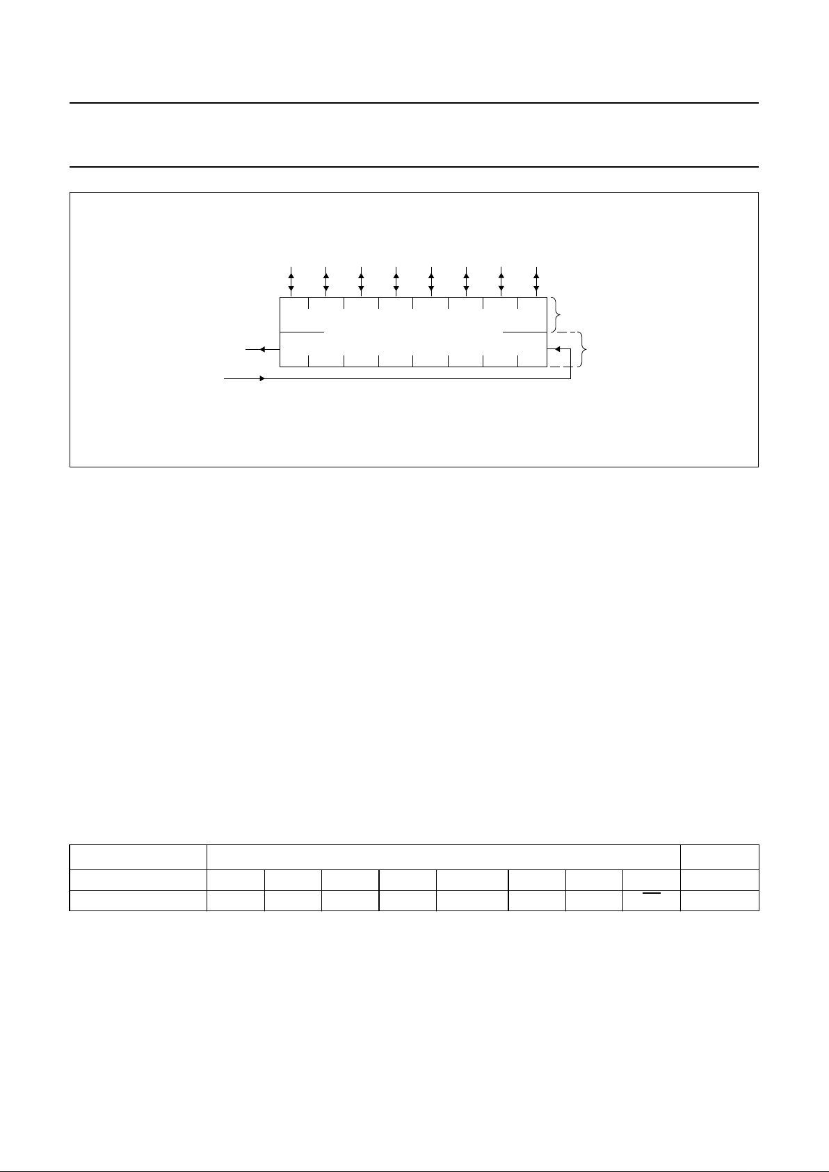
4 BLOCK DIAGRAM
Fig.1 Block diagram.
(1) X = don’t care.
(2) Pin mnemonics between parenthesis indicate the 68000 mode pin designations.
(3) These pin mnemonics represent the long-distance mode pin designations.
handbook, full pagewidth
MBD908 - 1
DB6DB7 DB5 DB4 DB3 DB2 DB1 DB0
1415 13 12 11 9 8 7
READ BUFFER
SHIFT REGISTER
DATA SHIFT REGISTER S0 AND READ BUFFER
write
only
8
MSB
MSB LSB
COMPARATOR S0, S0'
OWN ADDRESS S0'
X
8
INTERRUPT VECTOR S3
8
CLOCK REGISTER S2
8
S20S21S22S23S24000
CLOCK REGISTER S2
8
ACKSTOSTAENIES2ES1ES0PIN
REGISTER S1
CONTROL STATUS
BBLABAAS
AD0/
LRB
BERSTS0PIN
write only
read only
REGISTER ACCESS CONTROL
BUS BUFFER CONTROL
INTERRUPT CONTROL
RESET/STROBE CONTROL
INT
SCL OUT
IACK
SDA IN
CLK
541
VV
DD SS
20 10
DATA CONTROL
DIGITAL
FILTER
SDA/
SDA OUT
2
SCL CONTROL
DIGITAL
FILTER
SCL/
SCL IN
3
PCF8584
RESET/ CS A0
19 17 6
STROBE
(O.C.)
WR (R/W)18RD (DTACK)
16
CLOCK PRESCALER
SCL MULTIPLEXER
BUS BUSY LOGIC
ARBITRATION LOGIC
X
PARALLEL BUS
CONTROL STATUS REGISTER S1
read
only
(1)
(1)
(3)
(3)
(2) (2)
(3) (3)
PARALLEL BUS CONTROL
default: 00H 80XX
0FH 68XXX
Page 5

1997 Oct 21 5
Philips Semiconductors Product specification
I2C-bus controller
PCF8584
5 PINNING
SYMBOL PIN I/O DESCRIPTION
CLK 1 I clock input from microcontroller clock generator (internal pull-up)
SDA or
SDA OUT
2 I/O I2C-bus serial data input/output (open-drain). Serial data output in long-distance
mode.
SCL or SCL IN 3 I/O I
2
C-serial clock input/output (open-drain). Serial clock input in long-distance mode.
IACK or
SDA IN
4 I Interrupt acknowledge input (internal pull-up); when this signal is asserted the
interrupt vector in register S3 will be available at the bus Port if the ENI flag is set.
Serial data input in long-distance mode.
INT or
SCL OUT
5 O Interrupt output (open-drain); this signal is enabled by the ENI flag in register S1.
It is asserted when the PIN flag is reset. (PIN is reset after 1 byte is transmitted or
received over the I2C-bus). Serial clock output in long-distance mode.
A0 6 I Register select input (internal pull-up); this input selects between the control/status
register and the other registers. Logic 1 selects register S1, logic 0 selects one of
the other registers depending on bits loaded in ESO, ES1 and ES2 of register S1.
DB0 7 I/O bidirectional 8-bit bus Port 0
DB1 8 I/O bidirectional 8-bit bus Port 1
DB2 9 I/O bidirectional 8-bit bus Port 2
V
SS
10 − ground
DB3 11 I/O bidirectional 8-bit bus Port 3
DB4 12 I/O bidirectional 8-bit bus Port 4
DB5 13 I/O bidirectional 8-bit bus Port 5
DB6 14 I/O bidirectional 8-bit bus Port 6
DB7 15 I/O bidirectional 8-bit bus Port 7
RD (DTACK) 16 I/(O) RD is the read control input for MAB8049, MAB8051 or Z80-types. DTACK is the
data transfer control output for 68000-types (open-drain).
CS 17 I chip select input (internal pull-up)
WR (R/W) 18 I WR is the write control input for MAB8048, MAB8051, or Z80-types
(internal pull-up). R/W control input for 68000-types.
RESET/
STROBE
19 I/O Reset input (open-drain); this input forces the I2C-bus controller into a predefined
state; all flags are reset, except PIN, which is set. Also functions as strobe output.
V
DD
20 − supply voltage
Page 6

1997 Oct 21 6
Philips Semiconductors Product specification
I2C-bus controller
PCF8584
6 FUNCTIONAL DESCRIPTION
6.1 General
The PCF8584 acts as an interface device between
standard high-speed parallel buses and the serial I
2
C-bus.
On the I2C-bus, it can act either as master or slave.
Bidirectional data transfer between the I2C-bus and the
parallel-bus microcontroller is carried out on a byte-wise
basis, using either an interrupt or polled handshake.
Interface to either 80XX-type (e.g. 8048, 8051, Z80) or
68000-type buses is possible. Selection of bus type is
automatically performed (see Section 6.2).
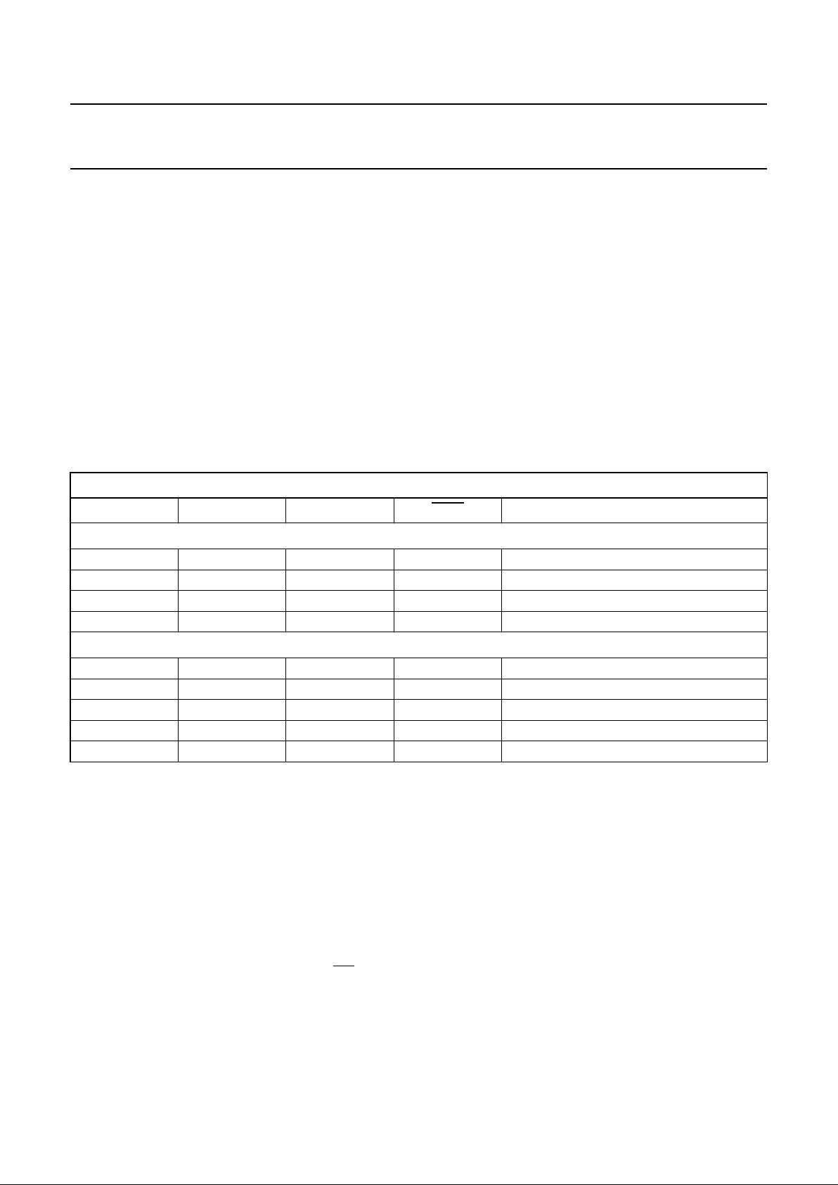
Fig.2 Pin configuration.
handbook, halfpage
CLK
SDA or SDA OUT
SCL or SCL IN
A0
DB0
DB1
DB2
V
SS
V
DD
DB7
DB6
DB5
DB4
DB3
1
2
3
4
5
6
7
8
9
10
20
19
18
17
16
15
14
13
12
11
PCF8584
MLA012 - 1
IACK or SDA IN
INT or SCL OUT
RESET / STROBE
CS
RD (DTACK)
WR (R/W)
(1)
(1)
(1) Pin mnemonics between parenthesis indicate the 68000 mode
pin designations.
Table 1 Control signals utilized by the PCF8584 for
microcontroller/microprocessor interfacing
The structure of the PCF8584 is similar to that of the
I
2
C-bus interface section of the Philips’
MABXXXX/PCF84(C)XX-series of microcontrollers, but
with a modified control structure. The PCF8584 has five
internal register locations. Three of these (own address
register S0', clock register S2 and interrupt vector S3) are
used for initialization of the PCF8584. Normally they are
only written once directly after resetting of the PCF8584.
The remaining two registers function as double registers
(data buffer/shift register S0, and control/status
register S1) which are used during actual data
transmission/reception. By using these double registers,
which are separately write and read accessible, overhead
for register access is reduced. Register S0 is a
combination of a shift register and data buffer.
Register S0 performs all serial-to-parallel interfacing with
the I2C-bus.
Register S1 contains I2C-bus status information required
for bus access and/or monitoring.
6.2 Interface Mode Control (IMC)
Selection of either an 80XX mode or 68000 mode
interface is achieved by detection of the first
WR-CS signal
sequence. The concept takes advantage of the fact that
the write control input is common for both types of
interfaces. An 80XX-type interface is default. If a
HIGH-to-LOW transition ofWR (R/W) is detected while CS
is HIGH, the 68000-type interface mode is selected and
theDTACK output is enabled. Care must be taken thatWR
and CS are stable after reset.
TYPE R/
W WR R DTACK IACK
8048/
8051
no yes yes no no
68000 yes no no yes yes
Z80 no yes yes no yes
Page 7
1997 Oct 21 7
Philips Semiconductors Product specification
I2C-bus controller
PCF8584
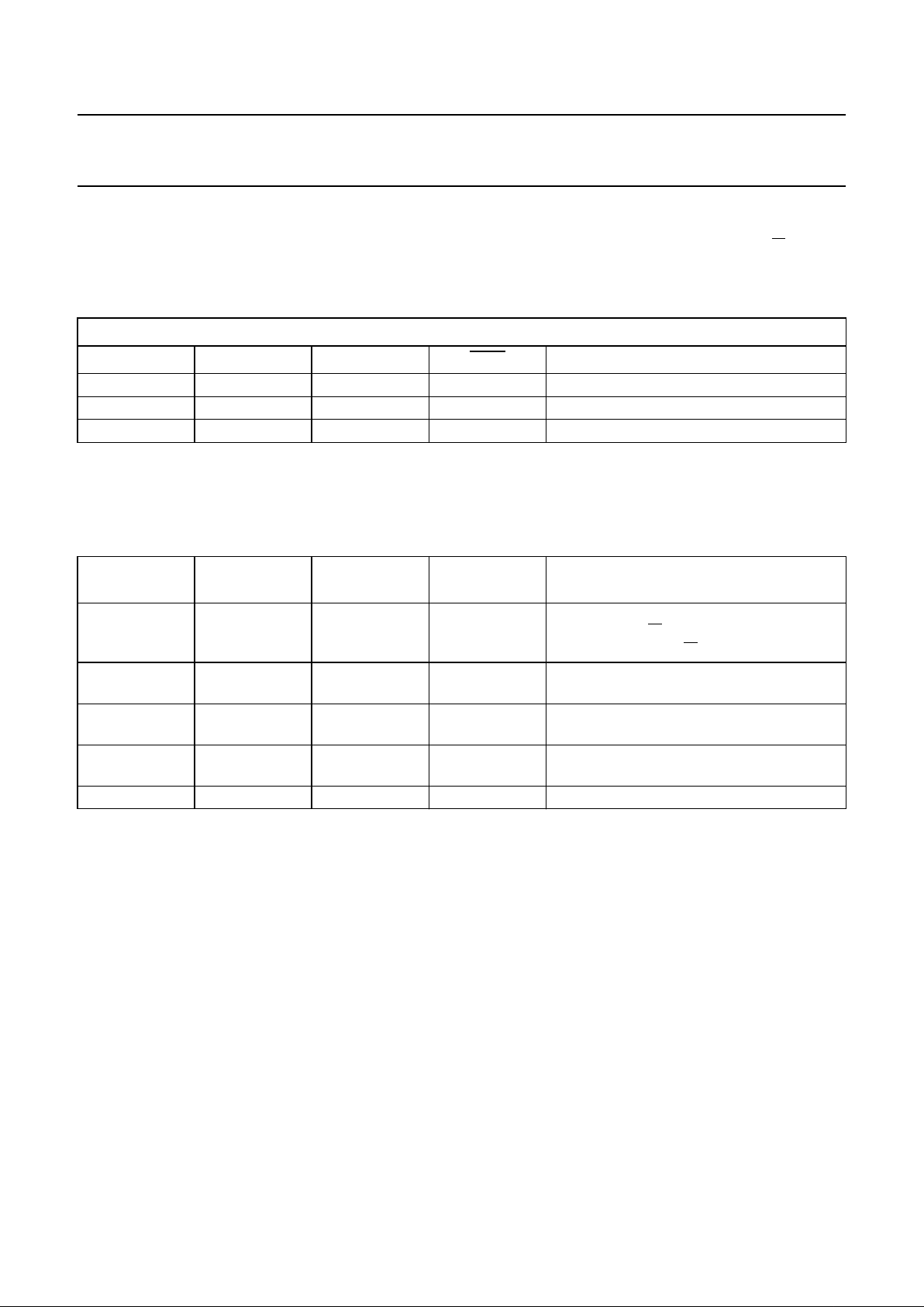
Fig.3 68000/80XX timing sequence utilized by the Interface Mode Control (IMC).
handbook, full pagewidth
FILTER
t = 16CLK
RESET
STROBE
D
EN
D
EN
ENRD
SIO DIVIDER
(S21 and S20)
DIVIDER
(S24, S23, S22)
/2, 3, 4, 5, 8
I2C-bus
(1.5 MHz)
CS A0
SCL
INT IACK CLK
(50 : 50)
WR/
R/W
RD/
DTACK
MBE706
handbook, full pagewidth
mode select
mode locked
R/W
CS
DTACK
mode select
WR
CS
MBE707
(1)
(2)
(1) Bus timing; 68000 mode write cycle.
(2) Bus timing; 80XX mode.
Page 8
1997 Oct 21 8
Philips Semiconductors Product specification
I2C-bus controller
PCF8584
6.3 Set-up registers S0', S2 and S3
Registers S0', S2 and S3 are used for initialization of the
PCF8584 (see Fig.5 ‘Initialization sequence’ flowchart).
6.4 Own address register S0'
When the PCF8584 is addressed as slave, this register
must be loaded with the 7-bit I
2
C-bus address to which the
PCF8584 is to respond. During initialization, the own
address register S0' must be written to, regardless
whether it is later used. The Addressed As Slave (AAS) bit
in status register S1 is set when this address is received
(the value in S0 is compared with the value in S0'). Note
that the S0 and S0' registers are offset by one bit; hence,
programming the own address register S0' with a value of
55H will result in the value AAH being recognized as the
PCF8584’s slave address (see Fig.1).
Programming of S0' is accomplished via the parallel-bus
when A0 is LOW, with the appropriate bit combinations set
in control status register S1 (S1 is written when
pin A0 = HIGH). Bit combinations for accessing all
registers are given in Table 5. After reset, S0' has default
address 00H (PCF8584 is thus initially in monitor mode,
see Section 6.12.3).
6.5 Clock register S2
Register S2 provides control over chip clock frequency
and SCL clock frequency. S20 and S21 provide a selection
of 4 different I
2
C-bus SCL frequencies which are shown in
Table 2. Note that these SCL frequencies are only
obtained when bits S24, S23 and S22 are programmed to
the correct input clock frequency (f
clk
).
Table 2 Register S2 selection of SCL frequency
S22, S23 and S24 are used for control of the internal clock
prescaler. Due to the possibility of varying microcontroller
clock signals, the prescaler can be programmed to adapt
to 5 different clock rates, thus providing a constant internal
clock. This is required to provide a stable time base for the
SCL generator and the digital filters associated with the
I
2
C-bus signals SCL and SDA. Selection for adaption to
external clock rates is shown in Table 3.
BIT
APPROXIMATE SCL
FREQUENCY f
SCL
(kHz)
S21 S20
00 90
01 45
10 11
1 1 1.5
Programming of S2 is accomplished via the parallel-bus
when A0 = LOW, with the appropriate bit combinations set
in control status register S1 (S1 is written when
A0 = HIGH). Bit combinations for accessing all registers
are given in Table 5.
Table 3 Register S2 selection of clock frequency
Note
1. X = don’t care.
6.6 Interrupt vector S3
The interrupt vector register provides an 8-bit
user-programmable vector for vectored-interrupt
microcontrollers. The vector is sent to the bus port
(DB7 to DB0) when an interrupt acknowledge signal is
asserted and the ENI (enable interrupt) flag is set. Default
vector values are:
• Vector is ‘00H’ in 80XX mode
• Vector is ‘0FH’ in 68000 mode.
On reset the PCF8584 is in the 80XX mode, thus the
default interrupt vector is ‘00H’.
6.7 Data shift register/read buffer S0
Register S0 acts as serial shift register and read buffer
interfacing to the I
2
C-bus. All read and write operations
to/from the I2C-bus are done via this register. S0 is a
combination of a shift register and a data buffer; parallel
data is always written to the shift register, and read from
the data buffer. I2C-bus data is always shifted in or out of
shift register S0.
INTERNAL CLOCK FREQUENCY
S24 S23 S22 f
clk
(MHz)
0X
(1)
X
(1)
3
1 0 0 4.43
1016
1108
11112
Page 9
1997 Oct 21 9
Philips Semiconductors Product specification
I2C-bus controller
PCF8584
In receiver mode the data from the shift register is copied to the read buffer during the acknowledge phase. Further
reception of data is inhibited (SCL held LOW) until the S0 read buffer is read (see Section 6.8.1.1).
In the transmitter mode data is transmitted to the I2C-bus as soon as it is written to the S0 shift register if the serial I/O is
enabled (ESO = 1).
Remarks:
1. A minimum of 6 clock cycles must elapse between consecutive parallel-bus accesses to the PCF8584 when the
I2C-bus controller operates at 8 or 12 MHz. This may be reduced to 3 clock cycles for lower operating frequencies.
2. To start a read operation immediately after a write, it is necessary to read the S0 read buffer in order to invoke
reception of the first byte (‘dummy read’ of the address). Immediately after the acknowledgement, this first byte will
be transferred from the shift register to the read buffer. The next read will then transfer the correct value of the first
byte to the microcontroller bus (see Fig.7).
6.8 Control/status register S1
Register S1 controls I
2
C-bus operation and provides I2C-bus status information. Register S1 is accessed by a HIGH
signal on register select input A0. For more efficient communication between microcontroller/processor and the I2C-bus,
register S1 has separate read and write functions for all bit positions (see Fig.3). The write-only section provides register
access control and control over I2C-bus signals, while the read-only section provides I2C-bus status information.
Table 4 Control/status register S1
Notes
1. For further information see Section 6.8.1.
2. For further information see Section 6.8.2.
3. Logic 1 if not-initialized.
CONTROL/STATUS BITS MODE
Control
(1)
PIN ESO ES1 ES2 ENI STA STO ACK write only
Status
(2)
PIN 0
(3)
STS BER AD0/LRB AAS LAB BB read only
Fig.4 Data shift register/bus buffer S0.
ndbook, full pagewidth
DB7 DB6 DB5 DB4 DB3 DB2 DB1 DB0
Read Buffer
Data Shift Register S0 and Read Buffer
Shift register
Read
only
Write
only
to/from
I
2
C-Bus SDA line
to/from microcontroller parallel bus
MBE705
Page 10
1997 Oct 21 10
Philips Semiconductors Product specification
I2C-bus controller
PCF8584
6.8.1 REGISTER S1 CONTROL SECTION
The write-only section of S1 enables access to registers S0, S0', S1, S2 and S3, and controls I2C-bus operation; see
Table 4.
6.8.1.1 PIN (Pending Interrupt Not)
When the PIN bit is written with a logic 1, all status bits are reset to logic 0. This may serve as a software reset function
(see Figs 5 to 9). PIN is the only bit in S1 which may be both read and written to. PIN is mostly used as a status bit for
synchronizing serial communication, see Section 6.8.2.
6.8.1.2 ESO (Enable Serial Output)
ESO enables or disables the serial I2C-bus I/O. When ESO is LOW, register access for initialization is possible. When
ESO is HIGH, I2C-bus communication is enabled; communication with serial shift register S0 is enabled and the S1 bus
status bits are made available for reading.
Table 5 Register access control; ESO = 0 (serial interface off) and ESO = 1 (serial interface on)
Notes
1. With ESO = 0, bits ENI, STA, STO and ACK of S1 can be read for test purposes.
2. ‘X’ if ENI = 0.
6.8.1.3 ES1 and ES2
ES1 and ES2 control selection of other registers for initialization and control of normal operation. After these bits are
programmed for access to the desired register (shown in Table 5), the register is selected by a logic LOW level on
register select pin A0.
6.8.1.4 ENI
This bit enables the external interrupt output INT, which is generated when the PIN bit is active (logic 0).
This bit must be set to logic 0 before entering the long-distance mode, and remain at logic 0 during operation in
long-distance mode.
INTERNAL REGISTER ADDRESSING 2-WIRE MODE
A0 ES1 ES2
IACK FUNCTION
ESO = 0; serial interface off (see note 1)
10X1
(2)
R/W S1: control
0001
(2)
R/W S0': (own address)
0011
(2)
R/W S3: (interrupt vector)
0101
(2)
R/W S2: (clock register)
ESO = 1; serial interface on
1 0 X 1 W S1: control
1 0 X 1 R S1; status
0001R/WS0: (data)
0011R/WS3: (interrupt vector)
X 0 X 0 R S3: (interrupt vector ACK cycle))
Page 11
1997 Oct 21 11
Philips Semiconductors Product specification
I2C-bus controller
PCF8584
6.8.1.5 STA and STO
These bits control the generation of the I2C-bus START condition and transmission of slave address and R/W bit,
generation of repeated START condition, and generation of the STOP condition (see Table 7).
Table 6 Register access control; ESO = 1 (serial interface on) and ES1 = 1; long-distance (4-wire) mode; note 1
Note
1. Trying to read from or write to registers other than S0 and S1 (setting ESO = 0) brings the PCF8584 out of the
long-distance mode.
Table 7 Instruction table for serial bus control
Notes
1. In master receiver mode, the last byte must be terminated with ACK bit HIGH (‘negative acknowledge’).
2. If both STA and STO are set HIGH simultaneously in master mode, a STOP condition followed by a START
condition + address will be generated. This allows ‘chaining’ of transmissions without relinquishing bus control.
3. All other STA and STO mode combinations not mentioned in Table 7 are NOPs.
6.8.1.6 ACK
This bit must be set normally to a logic 1. This causes the I2C-bus controller to send an acknowledge automatically after
each byte (this occurs during the 9th clock pulse). The bit must be reset (to logic 0) when the I2C-bus controller is
operating in master/receiver mode and requires no further data to be sent from the slave transmitter. This causes a
negative acknowledge on the I2C-bus, which halts further transmission from the slave device.
6.8.2 R
EGISTER S1 STATUS SECTION
The read-only section of S1 enables access to I2C-bus status information; see Table 4.
INTERNAL REGISTER ADDRESSING: LONG-DISTANCE (4-WIRE) MODE
A0 ES1 ES2
IACK FUNCTION
1 1 X 1 W S1: control
1 1 X X R S1; status
0 1 X X R/W S0; (data)
STA STO
PRESENT
MODE
FUNCTION OPERATION
1 0 SLV/REC START transmit START + address, remain
MST/TRM if R/
W=0;
go to MST/REC if R/W=1
1 0 MST/TRM REPEAT
START
same as for SLV/REC
0 1 MST/REC;
MST/TRM
STOP READ;
STOP WRITE
transmit STOP go to SLV/REC mode; note 1
1 1 MST DATA
CHAINING
send STOP, START and address after last
master frame without STOP sent; note 2
0 0 ANY NOP no operation; note 3
Page 12

1997 Oct 21 12
Philips Semiconductors Product specification
I2C-bus controller
PCF8584
6.8.2.1 PIN bit
‘Pending Interrupt Not’ (MSB of register S1) is a status flag
which is used to synchronize serial communication and is
set to logic 0 whenever the PCF8584 requires servicing.
The PIN bit is normally read in polled applications to
determine when an I2C-bus byte transmission/reception is
completed. The PIN bit may also be written, see
Section 6.8.1.
Each time a serial data transmission is initiated (by setting
the STA bit in the same register), the PIN bit will be set to
logic 1 automatically (inactive). When acting as
transmitter, PIN is also set to logic 1 (inactive) each time
S0 is written. In receiver mode, the PIN bit is automatically
set to logic 1 (inactive) each time the data register S0 is
read.
After transmission or reception of one byte on the I
2
C-bus
(9 clock pulses, including acknowledge), the PIN bit will be
automatically reset to logic 0 (active) indicating a complete
byte transmission/reception. When the PIN bit is
subsequently set to logic 1 (inactive), all status bits will be
reset to logic 0. PIN is also set to zero on a BER (bus error)
condition.
In polled applications, the PIN bit is tested to determine
when a serial transmission/reception has been completed.
When the ENI bit (bit 4 of write-only section of register S1)
is also set to logic 1 the hardware interrupt is enabled.
In this case, the PIN flag also triggers an external interrupt
(active LOW) via the INT output each time PIN is reset to
logic 0 (active).
When acting as slave transmitter or slave receiver, while
PIN = 0, the PCF8584 will suspend I2C-bus transmission
by holding the SCL line LOW until the PIN bit is set to
logic 1 (inactive). This prevents further data from being
transmitted or received until the current data byte in S0 has
been read (when acting as slave receiver) or the next data
byte is written to S0 (when acting as slave transmitter).
PIN bit summary:
• The PIN bit can be used in polled applications to test
when a serial transmission has been completed. When
the ENI bit is also set, the PIN flag sets the external
interrupt via the INT output.
• Setting the STA bit (start bit) will set PIN = 1 (inactive).
• In transmitter mode, after successful transmission of
one byte on the I2C-bus the PIN bit will be automatically
reset to logic 0 (active) indicating a complete byte
transmission.
• In transmitter mode, PIN is set to logic 1 (inactive) each
time register S0 is written.
• In receiver mode, PIN is set to logic 0 (active) on
completion of each received byte. Subsequently, the
SCL line will be held LOW until PIN is set to logic 1.
• In receiver mode, when register S0 is read, PIN is set to
logic 1 (inactive).
• In slave receiver mode, an I
2
C-bus STOP condition will
set PIN = 0 (active).
• PIN = 0 if a bus error (BER) occurs.
6.8.2.2 STS
When in slave receiver mode, this flag is asserted when an
externally generated STOP condition is detected (used
only in slave receiver mode).
6.8.2.3 BER
Bus error; a misplaced START or STOP condition has
been detected. Resets BB (to logic 1; inactive), sets
PIN = 0 (active).
6.8.2.4 LRB/AD0
‘Last Received Bit’ or ‘Address 0 (General Call) bit’. This
status bit serves a dual function, and is valid only while
PIN = 0:
1. LRB holds the value of the last received bit over the
I2C-bus while AAS = 0 (not addressed as slave).
Normally this will be the value of the slave
acknowledgement; thus checking for slave
acknowledgement is done via testing of the LRB.
2. AD0; when AAS = 1 (‘Addressed As Slave’ condition),
the I2C-bus controller has been addressed as a slave.
Under this condition, this bit becomes the ‘AD0’ bit and
will be set to logic 1 if the slave address received was
the ‘general call’ (00H) address, or logic 0 if it was the
I2C-bus controller’s own slave address.
6.8.2.5 AAS
‘Addressed As Slave’ bit. Valid only when PIN = 0. When
acting as slave receiver, this flag is set when an incoming
address over the I2C-bus matches the value in own
address register S0' (shifted by one bit, see Section 6.4),
or if the I2C-bus ‘General Call’ address (00H) has been
received (‘General Call’ is indicated when AD0 status bit is
also set to logic 1, see Section 6.8.2.4).
6.8.2.6 LAB
‘Lost Arbitration’ Bit. This bit is set when, in multi-master
operation, arbitration is lost to another master on the
I2C-bus.
Page 13

1997 Oct 21 13
Philips Semiconductors Product specification
I2C-bus controller
PCF8584
6.8.2.7 BB
‘Bus Busy’ bit. This is a read-only flag indicating when the
I2C-bus is in use. A zero indicates that the bus is busy, and
access is not possible. This bit is set/reset (logic 1/logic 0)
by STOP/START conditions.
6.9 Multi-master operation
To avoid conflict between data and repeated START and
STOP operations, multi-master systems have some
limitations:
• When powering up multiple PCF8584s in multi-master
systems, the possibility exists that one node may power
up slightly after another node has already begun an
I
2
C-bus transmission; the Bus Busy condition will thus
not have been detected. To avoid this condition, a delay
should be introduced in the initialization sequence of
each PCF8584 equal to the longest I2C-bus
transmission, see flowchart ‘PCF8584 initialization’
(Fig.5).
6.10 Reset
A LOW level pulse on the
RESET (CLK must run) input
forces the I2C-bus controller into a well-defined state.
All flags in S1 are reset to logic 0, except the PIN flag and
the BB flag, which are set to logic 1. S0' and S3 are set
to 00H.
The RESET pin is also used for the STROBE output
signal. Both functions are separated on-chip by a digital
filter. The reset input signal has to be sufficiently long
(minimum 30 clock cycles) to pass through the filter.
The STROBE output signal is sufficiently short (8 clock
cycles) to be blocked by the filter. For more detailed
information on the strobe function see Section 6.12.
6.11 Comparison to the MAB8400 I
2
C-bus interface
The structure of the PCF8584 is similar to that of the
MAB8400 series of microcontrollers, but with a modified
control structure. Access to all I2C-bus control and status
registers is done via the parallel-bus port in conjunction
with register select input A0, and control bits ESO, ES1
and ES2.
6.11.1 D
ELETED FUNCTIONS
The following functions are not available in the PCF8584:
• Always selected (ALS flag)
• Access to the bit counter (BC0 to BC2)
• Full SCL frequency selection (2 bits instead of 5 bits)
• The non-acknowledge mode (ACK flag)
• Asymmetrical clock (ASC flag).
6.11.2
ADDED FUNCTIONS
The following functions either replace the deleted
functions or are completely new:
• Chip clock prescaler
• Assert acknowledge bit (ACK flag)
• Register selection bits (ES1 and ES2 flags)
• Additional status flags (BER, ‘bus error’)
• Automatic interface control between 80XX and
68000-type microcontrollers
• Programmable interrupt vector
• Strobe generator
• Bus monitor function
• Long-distance mode [non-I2C-bus mode (4-wire); only
for communication between parallel-bus processors
using the PCF8584 at each interface point].
6.12 Special function modes
6.12.1 STROBE
When the I2C-bus controller receives its own address (or
the ‘00H’ general call address) followed immediately by a
STOP condition (i.e. no further data transmitted after the
address), a strobe output signal is generated at the
RESET/STROBE pin (pin 19). The STROBE signal
consists of a monostable output pulse (active LOW),
8 clock cycles long (see Fig.9). It is generated after the
STOP condition is received, preceded by the correct slave
address. This output can be used as a bus access
controller for multi-master parallel-bus systems.
Page 14

1997 Oct 21 14
Philips Semiconductors Product specification
I2C-bus controller
PCF8584
6.12.2 LONG-DISTANCE MODE
The long-distance mode provides the possibility of
longer-distance serial communication between parallel
processors via two I2C-bus controllers. This mode is
selected by setting ES1 to logic 1 while the serial interface
is enabled (ESO = 1).
In this mode the I2C-bus protocol is transmitted over
4 unidirectional lines, SDA OUT, SCL IN, SDA IN and
SCL IN (pins 2, 3, 4 and 5). These communication lines
should be connected to line drivers/receivers
(example: RS422) for long-distance applications.
Hardware characteristics for long-distance transmission
are then given by the chosen standard. Control of data
transmission is the same as in normal I
2
C-bus mode. After
reading or writing data to shift register S0, long-distance
mode must be initialized by setting ESO and ES1 to
logic 1. Because the interrupt output INT is not available in
this operating mode, synchronization of data
transmission/reception must be polled via the PIN bit.
Remarks:
Before entering the long-distance mode, ENI must be
set to logic 0.
When powering up an PCF8584-node in long-distance
mode, the PCF8584 must be isolated from the 4-wire
bus via 3-state line drivers/receivers until the PCF8584
is properly initialized for long-distance mode. Failure to
implement this precaution will result in system
malfunction.
6.12.3 M
ONITOR MODE
When the 7-bit own address register S0' is loaded with all
zeros, the I2C-bus controller acts as a passive I2C monitor.
The main features of the monitor mode are:
• The controller is always selected.
• The controller is always in the slave receiver mode.
• The controller never generates an acknowledge.
• The controller never generates an interrupt request.
• A pending interrupt condition does not force SCL LOW.
•
BB is set to logic 0 after detection of a START condition,
and reset to logic 1 after a STOP condition.
• Received data is automatically transferred to the read
buffer.
• Bus traffic is monitored by the PIN bit, which is reset to
logic 0 after the acknowledge bit of an incoming byte has
been received, and is set to logic 1 as soon as the first
bit of the next incoming byte is detected. Reading the
data buffer S0 sets the PIN bit to logic 1. Data in the read
buffer is valid from PIN = 0 and during the next 8 clock
pulses (until next acknowledge).
• AAS is set to logic 1 at every START condition, and
reset at every 9th clock pulse.
7 SOFTWARE FLOWCHART EXAMPLES
7.1 Initialization
The flowchart of Fig.5 gives an example of a proper
initialization sequence of the PCF8584.
7.2 Implementation
The flowcharts (Figs 6 to 9) illustrate proper programming
sequences for implementing master transmitter, master
receive, and master transmitter, repeated start and master
receiver modes in polled applications.
Page 15

1997 Oct 21 15
Philips Semiconductors Product specification
I2C-bus controller
PCF8584
Fig.5 PCF8584 initialization sequence.
handbook, full pagewidth
START
A0 = HIGH
A0 = LOW
reset minimum
30 clock cycles
delay: wait a time
equal to the longest I
2
C
message to synchronize
BB-bit. (multimaster
systems only
send byte 80H
send byte 55H
PCF8584 resets to
slave receiver mode
parallel bus interface
determined by
PCF8584 (80XX/68XXX)
initialization of
PCF8584 completed
send byte A0H
send byte 1CH
send byte C1H
END
address line A0
power-on
A0 = HIGH
A0 = LOW
A0 = HIGH
A0 = HIGH enables data transfer to/from
register S1
A0 = LOW Access to all other registers
defined by the bit pattern in
register S1
Loads byte 80H into register S1'
i.e. next byte will be loaded into register S0'
(own address register); serial interface off.
Loads byte 55H into register S0';
effective own address becomes AAH.
Loads byte A0H into register S1, i.e. next byte
will be loaded into the clock control register S2.
Loads byte 1CH into register S2;
system clock is 12 MHz; SCL = 90 kHz.
Loads byte C1H into register S1; register enable
serial interface, set I
2
C-bus into idle mode;
SDA and SCL are HIGH. The next write or read
operation will be to/from data transfer register
S0 if A0 = LOW.
On power-on, if an PCF8584 node is powered-up
slightly after another node has already begun an
I
2
C-bus transmission, the bus busy condition will
not have been detected. Thus, introducing this
delay will insure that this condition will not occur.
MBE714
Page 16

1997 Oct 21 16
Philips Semiconductors Product specification
I2C-bus controller
PCF8584
Fig.6 PCF8584 master transmitter mode.
andbook, full pagewidth
START
read byte from S1 register
END
A0 = HIGH
is bus busy?
(BB = 0?)
yes
no
PIN bit = 0?
no
yes
slave
acknowledged?
(LRB = 0?)
yes
send byte 'slave address'
A0 = LOW
send C5H to control
register S1
Load 'slave address' into S0 register:
'slave address' = value of slave address
(7-bits + R/W = 0). After reset, default = '0'
n = 0 (data byte counter);
m = number of data bytes
to be transferred
read byte from S1 register
n = m
no
n = n + 1
send byte 'data'
yes
A0 = HIGH
PCF8584 remains in
master transmitter
mode if R/W bit of
'slave address' = 0
A0 = HIGH
A0 = LOW
Load 'data'
into bus
buffer register S0;
data is transmitted.
send byte C3H
transmission
completed
A0 = HIGH
Load C3 into the S1 control
register: PCF8584 generates
'STOP' condition.
PCF8584 goes into
slave receiver mode
Load C5H into S1. 'C5H' = PCF8584 generates
the 'START' condition and clocks out the slave
address and the clock pulse for slave acknowledgement.
Next byte(s) sent to the S0 register will be immediately
transferred over the I
2
C-bus.
Poll for transmission finished.
MBE715
Page 17

1997 Oct 21 17
Philips Semiconductors Product specification
I2C-bus controller
PCF8584
Fig.7 PCF8584 master receiver mode.
(1) The first read of the S0 register is a ‘dummy read’ of the slave address which should be discarded. The first read of the S0 register simultaneously
reads the current value of S0 and then transfers the first valid data byte from the I
2
C-bus to S0.
handbook, full pagewidth
A0 = LOW
Load 'Slave Address' into S0 register:
'Slave Address' = 7 bits + R/W = 1.
Is the I2C-bus busy?
PCF8584 generates 'START' condition,
sends out slave address + RD to I
2
C-bus and
generates 9th clock pulse for slave ACK.
Set-up software counters.
Set ACK bit S1 to 0 in
preparation for negative
acknowledgement.
PCF8584 generates
'STOP' condition.
PCF8584 goes into
slave receiver mode.
This command transfers
the final data byte from
the data buffer to accumulator.
Because the STOP condition
was previously executed, no
I
2
C-bus activity takes place.
This command simultaneously
receives the final data byte
from the I
2
C-bus and loads
it into register S0.
Neg. ACK is also sent.
is bus busy?
(BB = 0?)
START
END
send byte 'slave address' to S0
A0 = HIGH
read byte from S1 status register
A0 = HIGH
send byte C5H to S1 control register
A0 = HIGH
read byte from S1 status register
A0 = LOW
read data byte from S0 register
(1)
n = n + 1
n = 0 (data byte counter)
m = number of data bytes
to be read
yes
no
A0 = HIGH
send byte 40H to control register S1
A0 = LOW
read data byte from S0 register
(1)
A0 = HIGH
read byte from S1 status register
A0 = HIGH
send byte C3H to S1
A0 = LOW
read final data byte from S0 register
PIN = 0?
no
yes
slave ACK?
(LRB = 0?)
n = m − 1?
yes
no no
(an error
has occured)
PIN = 0?
yes
MGL009
Page 18

1997 Oct 21 18
Philips Semiconductors Product specification
I2C-bus controller
PCF8584
Fig.8 Master transmitter followed by repeated START and becoming master receiver.
dbook, full pagewidth
START
I2C-bus write routine
(master transmitter mode
excluding final STOP)
send byte 45H
send byte 'slave address'
I2C-bus read routine (master receiver mode)
END
PCF8584 configured as
master transmitter
PCF8584 configured as
master receiver
A0 = HIGH
A0 = LOW
Load 45H into the S1 register; PCF8584
generates the repeated 'START condition' only.
The current contents of register S0 is NOT
clocked out onto the I2C-bus.
The next byte sent to register S0 should be the
'slave address' + read bit.
Load 'slave address' into the S0 register. Once
loaded, it is automatically clocked out over the I
2
C-bus.
'Slave address' = slave address (7 bits) + R/W bit set '1'.
MBE712
Page 19

1997 Oct 21 19
Philips Semiconductors Product specification
I2C-bus controller
PCF8584
Fig.9 Slave receiver/slave transmitter modes.
handbook, full pagewidth
START
read byte from S1 register
END
TX
A0 = HIGH
A0 = LOW
addressed as slave
(AAS = 1?)
no
yes
read byte from S1 register
PIN bit = 0?
yes
no
read byte from S0 register
read or write?
(LSB = 1 or 0?)
read byte from S1 register
PIN bit = 0?
R/W = 1
SLAVE
TRANSMITTER
MODE
no
yes
negative
ACK received?
(LRB = 1?)
yes
no
write last data byte
to S0 register
A0 = HIGH
A0 = LOW
END
RX
read byte from S1 register
PIN bit = 0?
R/W = 0
SLAVE
RECEIVER
MODE
no
yes
STOP detected?
(STS = 1?)
yes
no
read last data byte
from S0 register
write data to S0 register read data from S0 register
PIN deactivated
(set to '1')
PCF8584 goes into
slave receiver
mode
Read incoming address to
determine if the R/W bit is 0 or 1
This will differentiate between
slave receiver or slave
transmitter modes.
Check that 'own address'
has arrived correctly
Check whether
'addressed as slave'
MBE713
Page 20

1997 Oct 21 20
Philips Semiconductors Product specification
I2C-bus controller
PCF8584
8I2C-BUS TIMING DIAGRAMS
The diagrams (Figs 10 to 13) illustrate typical timing diagrams for the PCF8584 in master/slave functions. For detailed
description of the I2C-bus protocol, please refer to
“The I2C-bus and how to use it”
; Philips document
ordering number 9398 393 40011.
Fig.10 Bus timing diagram; master transmitter mode.
handbook, full pagewidth
MBE709
STOP
condition
interrupt
ACK
nbyte
ACK
interruptfirst-byte (E4H)interrupt
R/W = 0
ACK
7-bit address (76H)
START
condition
from slave receiver
SDA
SCL
INT
Master PCF8584 writes data to slave transmitter.
Fig.11 Bus timing diagram; master receiver mode.
handbook, full pagewidth
MBE710
STOP
condition
no ACK
nbyte
ACK
interruptfirst-byte (discard)interrupt
R/W = 1
ACK
7-bit address (76H)
START
condition
from slave
SDA
SCL
INT
'DUMMY READ'
must be executed here
from master
receiver
Master PCF8584 reads data from slave transmitter.
Page 21

1997 Oct 21 21
Philips Semiconductors Product specification
I2C-bus controller
PCF8584
Fig.12 Bus timing diagram; slave transmitter mode.
handbook, full pagewidth
MBE711
STOP
condition
no ACK
nbyte
ACK
interruptfirst-byte: 1FHinterrupt
R/W = 1
ACK
7-bit address (0CH)
START
condition
from slave PCF8584
SDA
SCL
INT
from master
receiver
interrupt
External master receiver reads data from PCF8584.
Fig.13 Bus timing diagram; slave receiver mode.
handbook, full pagewidth
MBE708
interrupt
(after STOP)
STOP
condition
interrupt
ACK
nbyte
ACK
interruptfirst-byte (CCH)interrupt
R/W = 0
ACK
7-bit address (62H)
START
condition
from slave PCF8584
SDA
SCL
INT
Slave PCF8584 is written to by external master transmitter.
Page 22

1997 Oct 21 22
Philips Semiconductors Product specification
I2C-bus controller
PCF8584
9 LIMITING VALUES
In accordance with the Absolute Maximum Rating System (IEC 134).
10 HANDLING
Inputs and outputs are protected against electrostatic discharge in normal handling. However, to be totally safe, it is good
practice to take normal precautions appropriate to handling MOS devices (see
“Handling MOS Devices”
).
SYMBOL PARAMETER MIN. MAX. UNIT
V
DD
supply voltage −0.3 +7.0 V
V
I
voltage range (any input) −0.8 VDD+ 0.5 V
I
I
DC input current (any input) −10 +10 mA
I
O
DC output current (any output) −10 +10 mA
P
tot
total power dissipation − 300 mW
P
O
power dissipation per output − 50 mW
T
amb
operating ambient temperature −40 +85 °C
T
stg
storage temperature −65 +150 °C
Page 23

1997 Oct 21 23
Philips Semiconductors Product specification
I2C-bus controller
PCF8584
11 DC CHARACTERISTICS
V
DD
=5V±10%; T
amb
= −40 to +85 °C; unless otherwise specified.
Notes
1. Test conditions: 22 kΩ pull-up resistors on D0 to D7; 10 kΩ pull-up resistors on SDA, SCL,
RD; RESET connected
to VSS; remaining pins open-circuit.
2. CLK waveform of 12 MHz with 50% duty factor.
3. CLK, IACK, A0, CS, WR, RD, RESET and D0 to D7 are TTL level inputs.
4. SDA and SCL are CMOS level inputs.
5. CLK, IACK, A0, CS and WR.
6. D0 to D7.
7. DTACK, STROBE.
8. D0 to D7 3-state, SDA, SCL, INT, RD, RESET.
SYMBOL PARAMETER CONDITIONS MIN. TYP. MAX. UNIT
Supply
V
DD
supply voltage 4.5 5.0 5.5 V
I
DD
supply current standby; note 1 −−2.5 µA
operating; notes 1 and 2 −−1.5 mA
Inputs
CLK,
IACK, A0, CS, WR, RD, RESET AND D0 to D7
V
IL
LOW level input voltage note 3 0 − 0.8 V
V
IH
HIGH level input voltage note 3 2.0 − V
DD
V
SDA AND SCL
V
IL
LOW level input voltage note 4 0 − 0.3V
DD
V
V
IH
HIGH level input voltage note 4 0.7V
DD
− V
DD
V
R
i
resistance to V
DD
T
amb
=25°C; note 5 25 − 100 kΩ
Outputs
I
OH
HIGH level output current VOH= 2.4 V; note 6 and 7 −2.4 −−mA
I
OL
LOW level output current VOL= 0.4 V; note 6 3.0 −−mA
I
OL
leakage current note 8 −1 − +1 µA
Page 24

1997 Oct 21 24
Philips Semiconductors Product specification
I2C-bus controller
PCF8584
12 I2C-BUS TIMING SPECIFICATIONS
All the timing limits are valid within the operating supply voltage and ambient temperature range; VDD=5V±10%;
T
amb
= −40 to +85 °C; and refer to VIL and VIHwith an input voltage of VSSto V
DD.
13 PARALLEL INTERFACE TIMING
All the timing limits are valid within the operating supply voltage and ambient temperature range: VDD=5V±10%;
T
amb
= −40 to +85 °C; and refer to VIL and VIHwith an input voltage of VSSto VDD. CL= 100 pF; RL= 1.5 kΩ
(connected to VDD) for open-drain and high-impedance outputs, where applicable (for measurement purposes only).
SYMBOL PARAMETER MIN. TYP. MAX. UNIT
f
SCL
SCL clock frequency −− 100 kHz
t
SW
tolerable spike width on bus −− 100 ns
t
BUF
bus free time 4.7 −−µs
t
SU;STA
START condition set-up time 4.7 −−µs
t
HD;STA
START condition hold time 4.0 −−µs
t
LOW
SCL LOW time 4.7 −−µs
t
HIGH
SCL HIGH time 4.0 −−µs
t
r
SCL and SDA rise time −− 1.0 µs
t
f
SCL and SDA fall time −− 0.3 µs
t
SU;DAT
data set-up time 250 −−ns
t
HD;DAT
data hold time 0 −−ns
t
VD;DAT
SCL LOW to data out valid −− 3.4 µs
t
SU;STO
STOP condition set-up time 4.0 −−µs
SYMBOL PARAMETER CONDITIONS MIN. TYP. MAX. UNIT
t
r
clock rise time see Fig.14 −− 6ns
t
f
clock fall time see Fig.14 −− 6ns
t
CLK
input clock period
(50% ±5% duty factor)
see Fig.14 83 − 333 ns
t
CLRL
CS set-up to RD LOW see Fig.16 and note 1 20 −−ns
t
CLWL
CS set-up to WR LOW see Fig.15 and note 1 20 −−ns
t
RHCH
CS hold from RD HIGH see Fig.16 0 −−ns
t
WHCH
CS hold from WR HIGH see Fig.15 0 −−ns
t
AVWL
A0 set-up to WR LOW see Fig.15 10 −−ns
t
AVRL
A0 set-up to RD LOW see Fig.16 10 −−ns
t
WHAI
A0 hold from WR HIGH see Fig.15 20 −−ns
t
RHAI
A0 hold from RD HIGH see Fig.16 10 −−ns
t
WLWH
WR pulse width see Fig.15 230 − 1000 ns
t
RLRH
RD pulse width see Fig.16 230 − 1000 ns
t
DVWH
data set-up before WR HIGH see Fig.15 150 −−ns
t
RLDV
data valid after RD LOW see Fig.16 − 160 180 ns
t
WHDI
data hold after WR HIGH see Fig.15 20 −−ns
t
RHDF
data bus floating after RD
HIGH
see Fig.16 −− 150 ns
Page 25

1997 Oct 21 25
Philips Semiconductors Product specification
I2C-bus controller
PCF8584
Notes
1. A minimum of 6 clock cycles must elapse between consecutive parallel-bus accesses when the I2C-bus controller
operates at 8 or 12 MHz. This may be reduced to 3 clock cycles for lower operating frequencies.
2. Not for S1.
t
AVCL
A0 set-up to CS LOW see Figs 17 and 18 10 −−ns
t
WLCL
R/WR set-up to CS LOW see Fig.17 10 −−ns
t
RHCL
R/WR set-up to CS LOW see Fig.18 10 −−ns
t
CLDV
data valid after CS LOW see Fig.18 and note 2 − 160 180 ns
t
CLDL
DT ACK LOW after CS LOW see Figs 17 and 18 − 2t
CLK
+75 3t
CLK
+ 150 ns
t
CHAI
A0 hold from CS HIGH see Fig.18 0 −−ns
t
CHRL
R/WR hold from CS HIGH see Fig.18 0 −−ns
t
CHWH
R/WR hold from CS HIGH see Fig.17 0 −−ns
t
CHDF
data bus float after CS HIGH see Fig.18 −− 150 ns
t
CHDE
DTACK HIGH from CS HIGH see Figs 17 and 18 − 100 120 ns
t
CHDI
data hold after CS HIGH see Fig.17 0 −−ns
t
DVCL
data set-up to CS LOW see Fig.17 0 −−ns
t
ALIE
INT HIGH from IACK LOW see Figs 19 and 20 − 130 180 ns
t
ALDV
data valid after IACK LOW see Figs 19 and 20 − 200 250 ns
t
ALAE
IACK pulse width see Fig.20 230 −−ns
t
AHDI
data hold after IACK HIGH see Fig.20 −− 30 ns
t
ALDL
DTACK LOW from IACK LOW see Fig.20 − 2t
CLK
+75 3t
CLK
+ 150 ns
t
AHDE
DTACK HIGH from IACK HIGH see Fig.20 − 120 140 ns
t
W4
RESET pulse width see Fig.21 30t
CLK
−−ns
t
W5
STROBE pulse width see Fig.22 8t
CLK
8t
CLK
+90 − ns
t
CLCL
CS LOW see Figs 17 and 18 − t
CLDL+tCHDE
− ns
SYMBOL PARAMETER CONDITIONS MIN. TYP. MAX. UNIT
Page 26

1997 Oct 21 26
Philips Semiconductors Product specification
I2C-bus controller
PCF8584
Fig.14 Clock input timing.
handbook, full pagewidth
t
CLK
35.5 ns
min
6 ns max 6 ns max
CLK
t
r
t
f
t
f
35.5 ns
min
MLA013 - 1
Fig.15 Bus timing (80XX mode); write cycle.
t
WLWH
t
AVWL
t
WHAI
t
CLWL
t
WHCH
A0
CS
WR
D0 to D7
MLA014 - 1
t
DVWH
t
WHDI
DATA VALID
Page 27

1997 Oct 21 27
Philips Semiconductors Product specification
I2C-bus controller
PCF8584
Fig.16 Bus timing (80XX mode); read cycle.
handbook, full pagewidth
t
RLRH
t
AVRL
t
RHAI
t
CLRL
t
RHCH
A0
CS
RD
D0 to D7
MLA015 - 1
t
RHDF
t
RLDV
DATA VALID
Fig.17 Bus timing (68000 mode); write cycle.
handbook, full pagewidth
MLA017 - 1
A0
D0 to D7
DATA VALID
t
CHAI
t
AVCL
t
WLCL
t
CLCL
t
CHWH
t
DVCL
t
CHDI
t
CLDL
t
CHDE
R/W
CS
DTACK
Page 28

1997 Oct 21 28
Philips Semiconductors Product specification
I2C-bus controller
PCF8584
Fig.18 Bus timing (68000 mode); read cycle.
MLA016 - 1
A0
D0 to D7
DATA VALID
t
CHAL
t
AVCL
t
RHCL
t
CLCL
t
CHRL
t
CLDV
t
CHDF
t
CLDL
t
CHDE
R/W
CS
DTACK
Fig.19 Interrupt timing (80XX mode).
t
ALIE
t
ALAE
t
ALDV
t
AHDI
DATA VALIDD0 to D7
IACK
INT
MLA018 - 1
Page 29

1997 Oct 21 29
Philips Semiconductors Product specification
I2C-bus controller
PCF8584
Fig.20 Interrupt timing (68000 mode).
handbook, full pagewidth
t
ALIE
t
ALAE
t
ALDL
t
AHDI
t
ALDV
t
AHDE
DATA VALIDD0 to D7
IACK
DTACK
INT
MLA019 - 1
Fig.21 Reset timing.
t
W4
CLK
RESET
MLA020 - 1
Page 30

1997 Oct 21 30
Philips Semiconductors Product specification
I2C-bus controller
PCF8584
Fig.22 Strobe timing.
CLK
t
W5
STROBE
MLA021 - 1
Page 31

1997 Oct 21 31
Philips Semiconductors Product specification
I2C-bus controller
PCF8584
14 APPLICATION INFORMATION
Fig.23 Application diagram using the 8048/8051.
DATA
WR
INT
RD
SCL
SDA
CS
A0
ALE
8048/8051
PCF8584
ADDRESS BUS
DECODER
MBE704
Page 32

1997 Oct 21 32
Philips Semiconductors Product specification
I2C-bus controller
PCF8584
Fig.24 Application diagram using the 68000.
AS
UDS
LDS
DECODER
ADDRESS
INTERRUPT
HANDLER
DATA
DTACK
R/W
SCL
SDA
CS
A1
A1, A2, A3
IACK
INT
FCX
IPX
68000
PCF8584
MBE702
Page 33

1997 Oct 21 33
Philips Semiconductors Product specification
I2C-bus controller
PCF8584
Fig.25 Application diagram using the 8088.
DATA
IOW
IOR
IACK
INTR
INT
SCL
SDA
CS
A0
ALE
8088
PCF8584
ADDRESS BUS
DECODER
MBE703
Page 34

1997 Oct 21 34
Philips Semiconductors Product specification
I2C-bus controller
PCF8584
14.1 Application notes
Additional application notes are available from Philips Semiconductors:
1. AN95068:
“C Routines for the PCF8584”.
2. AN96040:
“Using the PCF8584 with non-specified timings and other frequently asked questions”
.
3. AN90001:
“Interfacing PCF8584 I2C-bus controller to 80(C)51 family of microcontrollers”
.
Fig.26 PCF8584 diode protection.
Maximum forward current: 5 mA; maximum reverse voltage: 5 V.
handbook, full pagewidth
MBE701
1
2
3
4
5
6
7
8
9
10
20
19
18
17
16
15
14
13
12
11
Substrate
RESET/STROBE
WR (R/W)
CS
RD (DTACK)
DB7
DB6
DB5
DB4
DB3
V
DD
SDA or SDA OUT
SCL or SCL IN
IACK or SDA IN
INT or SCL OUT
A0
DB0
DB1
DB2
V
SS
CLK
(1)
Page 35

1997 Oct 21 35
Philips Semiconductors Product specification
I2C-bus controller
PCF8584
15 PACKAGE OUTLINES
UNIT
A
max.
1 2
b
1
cD E e M
H
L
REFERENCES
OUTLINE
VERSION
EUROPEAN
PROJECTION
ISSUE DATE
IEC JEDEC EIAJ
mm
inches
DIMENSIONS (inch dimensions are derived from the original mm dimensions)
SOT146-1
92-11-17
95-05-24
A
min.
A
max.
b
Z
max.
w
M
E
e
1
1.73
1.30
0.53
0.38
0.36
0.23
26.92
26.54
6.40
6.22
3.60
3.05
0.2542.54 7.62
8.25
7.80
10.0
8.3
2.04.2 0.51 3.2
0.068
0.051
0.021
0.015
0.014
0.009
1.060
1.045
0.25
0.24
0.14
0.12
0.010.10 0.30
0.32
0.31
0.39
0.33
0.0780.17 0.020 0.13
SC603
M
H
c
(e )
1
M
E
A
L
seating plane
A
1
w M
b
1
e
D
A
2
Z
20
1
11
10
b
E
pin 1 index
0 5 10 mm
scale
Note
1. Plastic or metal protrusions of 0.25 mm maximum per side are not included.
(1)
(1) (1)
DIP20: plastic dual in-line package; 20 leads (300 mil)
SOT146-1
Page 36

1997 Oct 21 36
Philips Semiconductors Product specification
I2C-bus controller
PCF8584
UNIT
A
max.
A
1
A2A
3
b
p
cD
(1)E(1) (1)
eHELLpQ
Z
ywv θ
REFERENCES
OUTLINE
VERSION
EUROPEAN
PROJECTION
ISSUE DATE
IEC JEDEC EIAJ
mm
inches
2.65
0.30
0.10
2.45
2.25
0.49
0.36
0.32
0.23
13.0
12.6
7.6
7.4
1.27
10.65
10.00
1.1
1.0
0.9
0.4
8
0
o
o
0.25 0.1
DIMENSIONS (inch dimensions are derived from the original mm dimensions)
Note
1. Plastic or metal protrusions of 0.15 mm maximum per side are not included.
1.1
0.4
SOT163-1
10
20
w M
b
p
detail X
Z
e
11
1
D
y
0.25
075E04 MS-013AC
pin 1 index
0.10
0.012
0.004
0.096
0.089
0.019
0.014
0.013
0.009
0.51
0.49
0.30
0.29
0.050
1.4
0.055
0.419
0.394
0.043
0.039
0.035
0.016
0.01
0.25
0.01
0.004
0.043
0.016
0.01
0 5 10 mm
scale
X
θ
A
A
1
A
2
H
E
L
p
Q
E
c
L
v M
A
(A )
3
A
SO20: plastic small outline package; 20 leads; body width 7.5 mm
SOT163-1
95-01-24
97-05-22
Page 37

1997 Oct 21 37
Philips Semiconductors Product specification
I2C-bus controller
PCF8584
16 SOLDERING
16.1 Introduction
There is no soldering method that is ideal for all IC
packages. Wave soldering is often preferred when
through-hole and surface mounted components are mixed
on one printed-circuit board. However, wave soldering is
not always suitable for surface mounted ICs, or for
printed-circuits with high population densities. In these
situations reflow soldering is often used.
This text gives a very brief insight to a complex technology.
A more in-depth account of soldering ICs can be found in
our
“IC Package Databook”
(order code 9398 652 90011).
16.2 DIP
16.2.1 SOLDERING BY DIPPING OR BY WAVE
The maximum permissible temperature of the solder is
260 °C; solder at this temperature must not be in contact
with the joint for more than 5 seconds. The total contact
time of successive solder waves must not exceed
5 seconds.
The device may be mounted up to the seating plane, but
the temperature of the plastic body must not exceed the
specified maximum storage temperature (T
stg max
). If the
printed-circuit board has been pre-heated, forced cooling
may be necessary immediately after soldering to keep the
temperature within the permissible limit.
16.2.2 R
EPAIRING SOLDERED JOINTS
Apply a low voltage soldering iron (less than 24 V) to the
lead(s) of the package, below the seating plane or not
more than 2 mm above it. If the temperature of the
soldering iron bit is less than 300 °C it may remain in
contact for up to 10 seconds. If the bit temperature is
between 300 and 400 °C, contact may be up to 5 seconds.
16.3 SO
16.3.1 REFLOW SOLDERING
Reflow soldering techniques are suitable for all SO
packages.
Reflow soldering requires solder paste (a suspension of
fine solder particles, flux and binding agent) to be applied
to the printed-circuit board by screen printing, stencilling or
pressure-syringe dispensing before package placement.
Several techniques exist for reflowing; for example,
thermal conduction by heated belt. Dwell times vary
between 50 and 300 seconds depending on heating
method. Typical reflow temperatures range from
215 to 250 °C.
Preheating is necessary to dry the paste and evaporate
the binding agent. Preheating duration: 45 minutes at
45 °C.
16.3.2 W
AVE SOLDERING
Wave soldering techniques can be used for all SO
packages if the following conditions are observed:
• A double-wave (a turbulent wave with high upward
pressure followed by a smooth laminar wave) soldering
technique should be used.
• The longitudinal axis of the package footprint must be
parallel to the solder flow.
• The package footprint must incorporate solder thieves at
the downstream end.
During placement and before soldering, the package must
be fixed with a droplet of adhesive. The adhesive can be
applied by screen printing, pin transfer or syringe
dispensing. The package can be soldered after the
adhesive is cured.
Maximum permissible solder temperature is 260 °C, and
maximum duration of package immersion in solder is
10 seconds, if cooled to less than 150 °C within
6 seconds. Typical dwell time is 4 seconds at 250 °C.
A mildly-activated flux will eliminate the need for removal
of corrosive residues in most applications.
16.3.3 R
EPAIRING SOLDERED JOINTS
Fix the component by first soldering two diagonallyopposite end leads. Use only a low voltage soldering iron
(less than 24 V) applied to the flat part of the lead. Contact
time must be limited to 10 seconds at up to 300 °C. When
using a dedicated tool, all other leads can be soldered in
one operation within 2 to 5 seconds between
270 and 320 °C.
Page 38

1997 Oct 21 38
Philips Semiconductors Product specification
I2C-bus controller
PCF8584
17 DEFINITIONS
18 LIFE SUPPORT APPLICATIONS
These products are not designed for use in life support appliances, devices, or systems where malfunction of these
products can reasonably be expected to result in personal injury. Philips customers using or selling these products for
use in such applications do so at their own risk and agree to fully indemnify Philips for any damages resulting from such
improper use or sale.
19 PURCHASE OF PHILIPS I
2
C COMPONENTS
Data sheet status
Objective specification This data sheet contains target or goal specifications for product development.
Preliminary specification This data sheet contains preliminary data; supplementary data may be published later.
Product specification This data sheet contains final product specifications.
Limiting values
Limiting values given are in accordance with the Absolute Maximum Rating System (IEC 134). Stress above one or
more of the limiting values may cause permanent damage to the device. These are stress ratings only and operation
of the device at these or at any other conditions above those given in the Characteristics sections of the specification
is not implied. Exposure to limiting values for extended periods may affect device reliability.
Application information
Where application information is given, it is advisory and does not form part of the specification.
Purchase of Philips I
2
C components conveys a license under the Philips’ I2C patent to use the
components in the I2C system provided the system conforms to the I2C specification defined by
Philips. This specification can be ordered using the code 9398 393 40011.
Page 39

1997 Oct 21 39
Philips Semiconductors Product specification
I2C-bus controller
PCF8584
NOTES
Page 40

Internet: http://www.semiconductors.philips.com
Philips Semiconductors – a worldwide company
© Philips Electronics N.V. 1997 SCA55
All rights are reserved. Reproduction in whole or in part is prohibited without the prior written consent of the copyright owner.
The information presented in this document does not form part of any quotation or contract, is believed to be accurate and reliable and may be changed
without notice. No liability will be accepted by the publisher for any consequence of its use. Publication thereof does not convey nor imply any license
under patent- or other industrial or intellectual property rights.
Netherlands: Postbus 90050, 5600 PB EINDHOVEN, Bldg. VB,
Tel. +31 40 27 82785, Fax. +31 40 27 88399
New Zealand: 2 Wagener Place, C.P.O. Box 1041, AUCKLAND,
Tel. +64 9 849 4160, Fax. +64 9 849 7811
Norway: Box 1, Manglerud 0612, OSLO,
Tel. +47 22 74 8000, Fax. +47 22 74 8341
Philippines: Philips Semiconductors Philippines Inc.,
106 Valero St. Salcedo Village, P.O. Box 2108 MCC, MAKATI,
Metro MANILA, Tel. +63 2 816 6380, Fax. +63 2 817 3474
Poland: Ul. Lukiska 10, PL 04-123 WARSZAWA,
Tel. +48 22 612 2831, Fax. +48 22 612 2327
Portugal: see Spain
Romania: see Italy
Russia: Philips Russia, Ul. Usatcheva 35A, 119048 MOSCOW,
Tel. +7 095 755 6918, Fax. +7 095 755 6919
Singapore: Lorong 1, Toa Payoh, SINGAPORE 1231,
Tel. +65 350 2538, Fax. +65 251 6500
Slovakia: see Austria
Slovenia: see Italy
South Africa: S.A. PHILIPS Pty Ltd., 195-215 Main Road Martindale,
2092 JOHANNESBURG, P.O. Box 7430 Johannesburg 2000,
Tel. +27 11 470 5911, Fax. +27 11 470 5494
South America: Rua do Rocio 220, 5th floor, Suite 51,
04552-903 São Paulo, SÃO PAULO - SP, Brazil,
Tel. +55 11 821 2333, Fax. +55 11 829 1849
Spain: Balmes 22, 08007 BARCELONA,
Tel. +34 3 301 6312, Fax. +34 3 301 4107
Sweden: Kottbygatan 7, Akalla, S-16485 STOCKHOLM,
Tel. +46 8 632 2000, Fax. +46 8 632 2745
Switzerland: Allmendstrasse 140, CH-8027 ZÜRICH,
Tel. +41 1 488 2686, Fax. +41 1 481 7730
Taiwan: Philips Semiconductors, 6F, No. 96, Chien Kuo N. Rd., Sec. 1,
TAIPEI, Taiwan Tel. +886 2 2134 2865, Fax. +886 2 2134 2874
Thailand: PHILIPS ELECTRONICS (THAILAND) Ltd.,
209/2 Sanpavuth-Bangna Road Prakanong, BANGKOK 10260,
Tel. +66 2 745 4090, Fax. +66 2 398 0793
Turkey: Talatpasa Cad. No. 5, 80640 GÜLTEPE/ISTANBUL,
Tel. +90 212 279 2770, Fax. +90 212 282 6707
Ukraine: PHILIPS UKRAINE, 4 Patrice Lumumba str., Building B, Floor 7,
252042 KIEV, Tel. +380 44 264 2776, Fax. +380 44 268 0461
United Kingdom: Philips Semiconductors Ltd., 276 Bath Road, Hayes,
MIDDLESEX UB3 5BX, Tel. +44 181 730 5000, Fax. +44 181 754 8421
United States: 811 East Arques Avenue, SUNNYVALE, CA 94088-3409,
Tel. +1 800 234 7381
Uruguay: see South America
Vietnam: see Singapore
Yugoslavia: PHILIPS, Trg N. Pasica 5/v, 11000 BEOGRAD,
Tel. +381 11 625 344, Fax.+381 11 635 777
For all other countries apply to: Philips Semiconductors, Marketing & Sales Communications,
Building BE-p, P.O. Box 218, 5600 MD EINDHOVEN, The Netherlands, Fax. +31 40 27 24825
Argentina: see South America
Australia: 34 Waterloo Road, NORTH RYDE, NSW 2113,
Tel. +61 2 9805 4455, Fax. +61 2 9805 4466
Austria: Computerstr. 6, A-1101 WIEN, P.O. Box 213, Tel. +43 160 1010,
Fax. +43 160 101 1210
Belarus: Hotel Minsk Business Center, Bld. 3, r. 1211, Volodarski Str. 6,
220050 MINSK, Tel. +375 172 200 733, Fax. +375 172 200 773
Belgium: see The Netherlands
Brazil: seeSouth America
Bulgaria: Philips Bulgaria Ltd., Energoproject, 15thfloor,
51 James Bourchier Blvd., 1407 SOFIA,
Tel. +359 2 689 211, Fax. +359 2 689 102
Canada: PHILIPS SEMICONDUCTORS/COMPONENTS,
Tel. +1 800 234 7381
China/Hong Kong: 501 Hong Kong Industrial Technology Centre,
72 Tat Chee Avenue, Kowloon Tong, HONG KONG,
Tel. +852 2319 7888, Fax. +852 2319 7700
Colombia: see South America
Czech Republic: see Austria
Denmark: Prags Boulevard 80, PB 1919, DK-2300 COPENHAGEN S,
Tel. +45 32 88 2636, Fax. +45 31 57 0044
Finland: Sinikalliontie 3, FIN-02630 ESPOO,
Tel. +358 9 615800, Fax. +358 9 61580920
France: 4 Rue du Port-aux-Vins, BP317, 92156 SURESNES Cedex,
Tel. +33 1 40 99 6161, Fax. +33 1 40 99 6427
Germany: Hammerbrookstraße 69, D-20097 HAMBURG,
Tel. +49 40 23 53 60, Fax. +49 40 23 536 300
Greece: No. 15, 25th March Street, GR 17778 TAVROS/ATHENS,
Tel. +30 1 4894 339/239, Fax. +30 1 4814 240
Hungary: seeAustria
India: Philips INDIA Ltd, Band Box Building, 2nd floor,
254-D, Dr. Annie Besant Road, Worli, MUMBAI 400 025,
Tel. +91 22 493 8541, Fax. +91 22 493 0966
Indonesia: see Singapore
Ireland: Newstead, Clonskeagh, DUBLIN 14,
Tel. +353 1 7640 000, Fax. +353 1 7640 200
Israel: RAPAC Electronics, 7 Kehilat Saloniki St, PO Box 18053,
TEL AVIV 61180, Tel. +972 3 645 0444, Fax. +972 3 649 1007
Italy: PHILIPS SEMICONDUCTORS, Piazza IV Novembre 3,
20124 MILANO, Tel. +39 2 6752 2531, Fax. +39 2 6752 2557
Japan: Philips Bldg 13-37, Kohnan 2-chome, Minato-ku, TOKYO 108,
Tel. +81 3 3740 5130, Fax. +81 3 3740 5077
Korea: Philips House, 260-199 Itaewon-dong, Yongsan-ku, SEOUL,
Tel. +82 2 709 1412, Fax. +82 2 709 1415
Malaysia: No. 76 Jalan Universiti, 46200 PETALING JAYA, SELANGOR,
Tel. +60 3 750 5214, Fax. +60 3 757 4880
Mexico: 5900 Gateway East, Suite 200, EL PASO, TEXAS 79905,
Tel. +9-5 800 234 7381
Middle East: see Italy
Printed in The Netherlands 417067/00/04/pp40 Date of release: 1997 Oct 21 Document order number: 9397 750 02932
 Loading...