

Page 1
INTEGRATED CIRCUITS
DATA SH EET
PCF8578
LCD row/column driver for dot
matrix graphic displays
Product specification
Supersedes data of 1997 Mar 28
File under Integrated Circuits, IC12
1998 Sep 08
Page 2

Philips Semiconductors Product specification
LCD row/column driver for dot matrix
graphic displays
CONTENTS
1 FEATURES
2 APPLICATIONS
3 GENERAL DESCRIPTION
4 ORDERING INFORMATION
5 BLOCK DIAGRAM
6 PINNING
7 FUNCTIONAL DESCRIPTION
7.1 Mixed mode
7.2 Row mode
7.3 Multiplexed LCD bias generation
7.4 Power-on reset
7.5 Internal clock
7.6 External clock
7.7 Timing generator
7.8 Row/column drivers
7.9 Display mode controller
7.10 Display RAM
7.11 Data pointer
7.12 Subaddress counter
7.13 I2C-bus controller
7.14 Input filters
7.15 RAM access
7.16 Display control
7.17 TEST pin
8I
8.1 Command decoder
9 CHARACTERISTICS OF THE I2C-BUS
9.1 Bit transfer
9.2 Start and stop conditions
9.3 System configuration
9.4 Acknowledge
10 LIMITING VALUES
11 HANDLING
12 DC CHARACTERISTICS
13 AC CHARACTERISTICS
14 APPLICATION INFORMATION
15 CHIP DIMENSIONS AND BONDING PAD
16 CHIP-ON GLASS INFORMATION
17 PACKAGE OUTLINE
2
C-BUS PROTOCOL
LOCATIONS
PCF8578
18 SOLDERING
18.1 Introduction
18.2 Reflow soldering
18.3 Wave soldering
18.3.1 LQFP
18.3.2 VSO
18.3.3 Method (LQFP and VSO)
18.4 Repairing soldered joints
19 DEFINITIONS
20 LIFE SUPPORT APPLICATIONS
21 PURCHASE OF PHILIPS I2C COMPONENTS
1998 Sep 08 2
Page 3

Philips Semiconductors Product specification
LCD row/column driver for dot matrix
graphic displays
1 FEATURES
• Single chip LCD controller/driver
• Stand-alone or may be used with up to 32 PCF8579s
(40960 dots possible)
• 40 driver outputs, configurable as32⁄8,24⁄16,16⁄24 or
8
⁄32rows/columns
• Selectable multiplex rates; 1 : 8, 1 : 16, 1 : 24 or 1 : 32
• Externally selectable bias configuration, 5 or 6 levels
• 1280-bit RAM for display data storage and scratch pad
• Display memory bank switching
• Auto-incremented data loading across hardware
subaddress boundaries (with PCF8579)
• Provides display synchronization for PCF8579
• On-chip oscillator, requires only 1 external resistor
• Power-on reset blanks display
• Logic voltage supply range 2.5 to 6 V
• Maximum LCD supply voltage 9 V
• Low power consumption
2
C-bus interface
• I
• TTL/CMOS compatible
• Compatible with most microcontrollers
• Optimized pinning for single plane wiring in multiple
device applications (with PCF8579)
• Space saving 56-lead plastic mini-pack and 64 pin quad
flat pack
• Compatible with chip-on-glass technology.
PCF8578
2 APPLICATIONS
• Automotive information systems
• Telecommunication systems
• Point-of-sale terminals
• Computer terminals
• Instrumentation.
3 GENERAL DESCRIPTION
The PCF8578 is a low power CMOS LCD row/column
driver, designed to drive dot matrix graphic displays at
multiplex rates of 1 : 8, 1 : 16, 1 : 24 or 1 : 32. The device
has 40 outputs, of which 24 are programmable,
configurable as
The PCF8578 can function as a stand-alone LCD
controller/driver for use in small systems, or for larger
systems can be used in conjunction with up to
32 PCF8579s for which it has been optimized. Together
these two devices form a general purpose LCD dot matrix
driver chip set, capable of driving displays of up to
40960 dots. The PCF8578 is compatible with most
microcontrollers and communicates via a two-line
bidirectional bus (I2C-bus). Communication overheads are
minimized by a display RAM with auto-incremented
addressing and display bank switching.
32
⁄8,24⁄16,16⁄24 or8⁄32rows/columns.
4 ORDERING INFORMATION
TYPE NUMBER
NAME DESCRIPTION VERSION
PCF8578T VSO56 plastic very small outline package; 56 leads SOT190-1
PCF8578U/2 − chip with bumps in tray −
PCF8578H LQFP64 plastic low profile quad flat package; 64 leads; body 10 × 10 × 1.4 mm SOT314-2
1998 Sep 08 3
PACKAGE
Page 4
Philips Semiconductors Product specification
LCD row/column driver for dot matrix
graphic displays
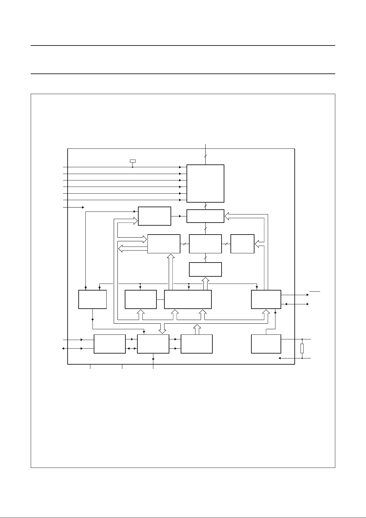
5 BLOCK DIAGRAM
9 (20)
V
DD
10 (21)
V
2
11 (22)
V
3
12 (23)
V
4
13 (24)
V
5
LCD
14 (25)
6 (12)
DISPLAY
MODE
CONTROLLER
V
TEST
C39 - C32
R31/C31 - R8/C8
R7 - R0
17 - 56
(29 to 35, 37, 38 to 46
48 to 62, 63, 64, 1 to 6)
ROW/COLUMN
DRIVERS
OUTPUT
CONTROLLER
PCF8578
(1)
PCF8578
SCL
SDA
POWER-ON
2 (8)
1 (7)
15, 16
RESET
INPUT
FILTERS
(14, 15, 17 to 19
26 to 28 36, 47)
n.c. n.c.
SUBADDRESS
COUNTER
2
I C-BUS
CONTROLLER
SA0
Y DECODER
AND SENSING
AMPLIFIERS
RAM DATA POINTER
7 (13)
32 x 40-BIT
DISPLAY RAM
X DECODER
YX
COMMAND
DECODER
DISPLAY
DECODER
TIMING
GENERATOR
OSCILLATOR
(9) 3
(10) 4
(16) 8
(11) 5
MSA842
R
SYNC
CLK
OSC
OSC
V
SS
(1) Operates at LCD voltage levels, all other blocks operate at logic levels.
The pin numbers given in parenthesis refer to the LQFP64 package.
Fig.1 Block diagram.
1998 Sep 08 4
Page 5

Philips Semiconductors Product specification
LCD row/column driver for dot matrix
graphic displays
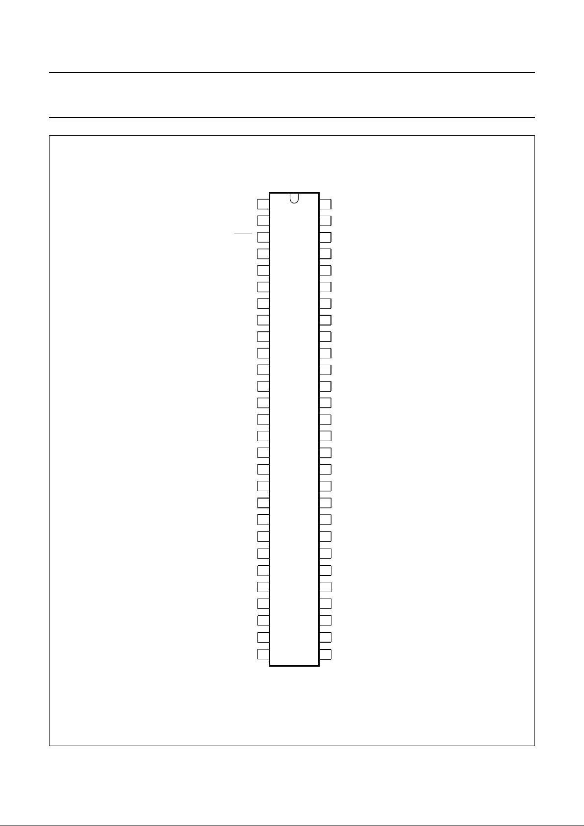
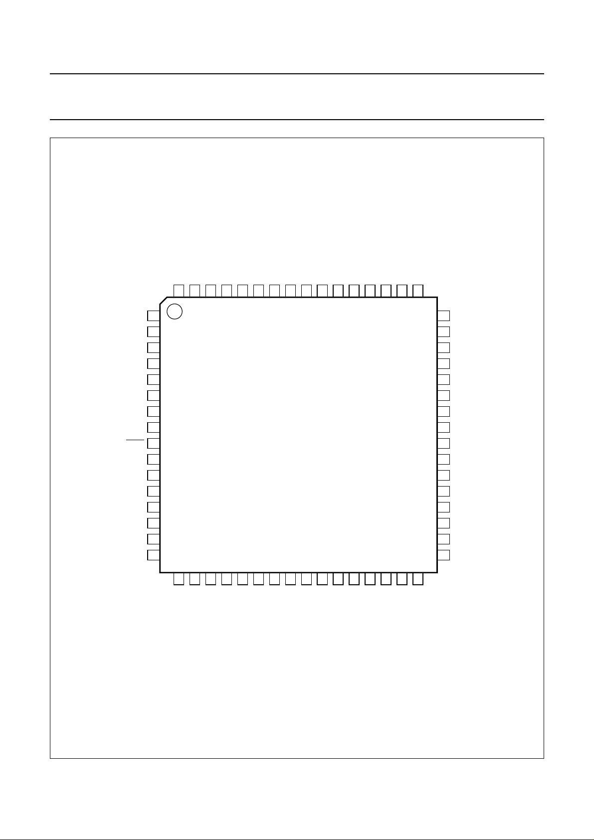
6 PINNING
SYMBOL
VSO56 LQFP64
SDA 1 7 I
SCL 2 8 I
SYNC 3 9 cascade synchronization output
CLK 4 10 external clock input/output
V
SS
5 11 ground (logic)
TEST 6 12 test pin (connect to V
SA0 7 13 I
OSC 8 16 oscillator input
V
V
V
DD
to V
2
LCD
5
9 20 positive supply voltage
10 to 13 21 to 24 LCD bias voltage inputs
14 25 LCD supply voltage
n.c. 15, 16 14, 15, 17 to 19,
C39 to C32 17 to 24 29 to 35, 37 LCD column driver outputs
R31/C31 to R8/C8 25 to 48 38 to 46, 48 to 62 LCD row/column driver outputs
R7 to R0 49 to 56 63, 64, 1 to 6 LCD row driver outputs
PIN
26 to 28, 36, 47
DESCRIPTION
2
C-bus serial data input/output
2
C-bus serial clock input
)
SS
2
C-bus slave address input (bit 0)
not connected
PCF8578
1998 Sep 08 5
Page 6
Philips Semiconductors Product specification
LCD row/column driver for dot matrix
graphic displays
SDA
1
2
SCL
SYNC
3
CLK
4
V
5
SS
TEST
6
SA0
7
OSC
8
V
9
DD
V
10
2
V
11
3
V
12
4
V
5
13
V
14
LCD
n.c.
n.c.
C39
C38
C37
C36
C35
C34
C33
C32
R31/C31
R30/C30
R29/C29
R28/C28
15
16
17
18
19
20
21
22
23
24
25
26
27
28
PCF8578
56
55
54
53
52
51
50
49
48
47
46
45
44
43
42
41
40
39
38
37
36
35
34
33
32
31
30
29
PCF8578
R0
R1
R2
R3
R4
R5
R6
R7
R8/C8
R9/C9
R10/C10
R11/C11
R12/C12
R13/C13
R14/C14
R15/C15
R16/C16
R17/C17
R18/C18
R19/C19
R20/C20
R21/C21
R22/C22
R23/C23
R24/C24
R25/C25
R26/C26
R27/C27
Fig.2 Pin configuration (VSO56).
1998 Sep 08 6
MSA839
Page 7
Philips Semiconductors Product specification
LCD row/column driver for dot matrix
graphic displays
handbook, full pagewidth
R6
R5
R4
R3
R2
R1
R0
SDA
SCL
SYNC
CLK
V
SS
TEST
SA0
n.c.
n.c.
OSC
R7
64
63
1
2
3
4
5
6
7
8
9
10
11
12
13
14
15
16
R8/C8
62
R9/C9
61
R11/C11
R10/C10
60
59
R13/C13
R12/C12
58
57
PCF8578
R15/C15
R14/C14
56
55
R17/C17
R16/C16
54
53
R19/C19
R18/C18
52
51
R21/C21
R20/C20
50
49
48
47
46
45
44
43
42
41
40
39
38
37
36
35
34
33
PCF8578
R22/C22
n.c.
R23/C23
R24/C24
R25/C25
R26/C26
R27/C27
R28/C28
R29/C29
R30/C30
R31/C31
C32
n.c.
C33
C34
C35
17
18
19
20
21
22
23
n.c.
n.c.
n.c.
DD
V
Fig.3 Pin configuration (LQFP64).
1998 Sep 08 7
24
25
26
27
28
29
30
31
32
5V4V3V2
V
LCD
V
n.c.
n.c.
n.c.
C39
C38
C37
MBH588
C36
Page 8
Philips Semiconductors Product specification
LCD row/column driver for dot matrix
graphic displays
7 FUNCTIONAL DESCRIPTION
The PCF8578 row/column driver is designed for use in one
of three ways:
• Stand-alone row/column driver for small displays
(mixed mode)
• Row/column driver with cascaded PCF8579s
(mixed mode)
• Row driver with cascaded PCF8579s (mixed mode).
7.1 Mixed mode
In mixed mode, the device functions as both a row and
column driver. It can be used in small stand-alone
applications, or for larger displays with up to 15 PCF8579s
(31 PCF8579s when two slave addresses are used).
See Table 1 for common display configurations.
7.2 Row mode
In row mode, the device functions as a row driver with up
to 32 row outputs and provides the clock and
synchronization signals for the PCF8579. Up to 16
PCF8579s can normally be cascaded (32 when two slave
addresses are used).
PCF8578
Timing signals are derived from the on-chip oscillator,
whose frequency is determined by the value of the resistor
connected between OSC and V
Commands sent on the I2C-bus from the host
microcontroller set the mode (row or mixed), configuration
(multiplex rate and number of rows and columns) and
control the operation of the device. The device may have
one of two slave addresses. The only difference between
these slave addresses is the least significant bit, which is
set by the logic level applied to SA0. The PCF8578 and
PCF8579 also have subaddresses. The subaddress of the
PCF8578 is only defined in mixed mode and is fixed at 0.
The RAM may only be accessed in mixed mode and data
is loaded as described for the PCF8579.
Bias levels may be generated by an external potential
divider with appropriate decoupling capacitors. For large
displays, bias sources with high drive capability should be
used. A typical mixed mode system operating with up to
15 PCF8579s is shown in Fig.5 (a stand-alone system
would be identical but without the PCF8579s).
SS
.
Table 1 Possible displays configurations
APPLICATION
MULTIPLEX
RATE
MIXED MODE ROW MODE
TYPICAL APPLICATIONS
ROWS COLUMNS ROWS COLUMNS
Stand alone 1 : 8 8 32 −−small digital or
1:16 16 24 −−
alphanumerical displays
1:24 24 16 −−
1:32 32 8 −−
With PCF8579 1 : 8 8
1:16 16
1:24 24
1:32 32
(1)
(1)
(1)
(1)
632
624
616
608
(1)
(1)
(1)
(1)
8 × 44
16 × 2
(2)
24
(2)
24
(2)
(2)
640
640
640
640
(2)
(2)
(2)
(2)
alphanumeric displays and
dot matrix graphic displays
Notes
1. Using 15 PCF8579s.
2. Using 16 PCF8579s.
1998 Sep 08 8
Page 9
Philips Semiconductors Product specification
LCD row/column driver for dot matrix
graphic displays
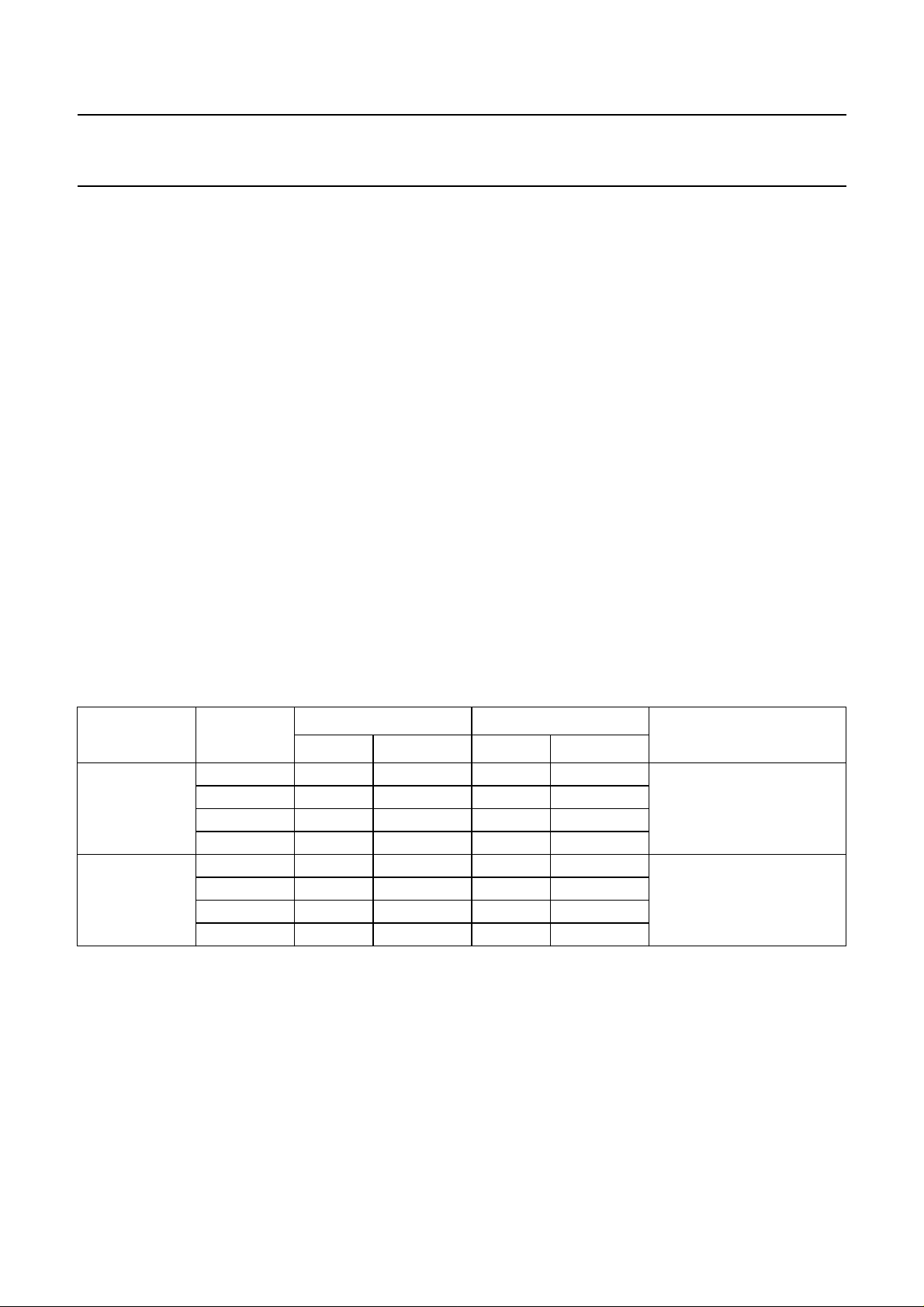
7.3 Multiplexed LCD bias generation
The bias levels required to produce maximum contrast
depend on the multiplex rate and the LCD threshold
voltage (Vth). Vth is typically defined as the RMS voltage at
which the LCD exhibits 10% contrast. Table 2 shows the
optimum voltage bias levels for the PCF8578 as functions
of Vop(Vop=VDD− V
ratios (D) for the different multiplex rates. A practical value
for Vop is obtained by equating V
shows the first 4 rows of Table 2 as graphs. Table 3 shows
the relative values of the resistors required in the
configuration of Fig.5 to produce the standard multiplex
rates.
Table 2 Optimum LCD voltages
PARAMETER
V
2
--------V
op
V
3
--------V
op
V
4
--------V
op
V
5
--------V
op
V
off rms()
----------------------V
op
V
on rms()
---------------------- V
op
V
on rms()
=
D
----------------------V
off rms()
), together with the discrimination
LCD
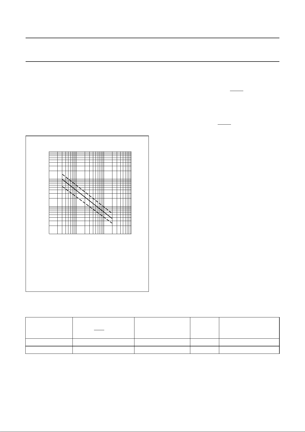
with Vth. Figure 4
off(rms)
MULTIPLEX RATE
1:8 1:16 1:24 1:32
0.739 0.800 0.830 0.850
0.522 0.600 0.661 0.700
0.478 0.400 0.339 0.300
0.261 0.200 0.170 0.150
0.297 0.245 0.214 0.193
0.430 0.316 0.263 0.230
1.447 1.291 1.230 1.196
PCF8578
7.4 Power-on reset
At power-on the PCF8578 resets to a defined starting
condition as follows:
1. Display blank
2. 1 : 32 multiplex rate, row mode
3. Start bank, 0 selected
4. Data pointer is set to X, Y address 0, 0
5. Character mode
6. Subaddress counter is set to 0
7. I2C-bus interface is initialized.
2
Data transfers on the I
following power-on, to allow completion of the reset action.
1.0
V
bias
V
op
0.8
0.6
0.4
0.2
0
V
Fig.4 V
, V3, V4, V5. See Table 2.
bias=V2
bias/Vop
C-bus should be avoided for 1 ms
MSA838
V
2
V
3
V
4
V
5
1:8 1:16 1:32
1:24
multiplex rate
as a function of the multiplex rate.
V
---------
V
op
th
3.370 4.080 4.680 5.190
Table 3 Multiplex rates and resistor values for Fig.5
MULTIPLEX RATE (n)
RESISTORS
n = 8 n = 16, 24, 32
R1 R R
R2 R
R3
n2–()R
3n–()R n3–()R
1998 Sep 08 9
Page 10
This text is here in white to force landscape pages to be rotated correctly when browsing through the pdf in the Acrobat reader.This text is here in
_white to force landscape pages to be rotated correctly when browsing through the pdf in the Acrobat reader.This text is here inThis text is here in
white to force landscape pages to be rotated correctly when browsing through the pdf in the Acrobat reader. white to force landscape pages to be ...
1998 Sep 08 10
LCD DISPLAY
Philips Semiconductors Product specification
LCD row/column driver for dot matrix
graphic displays
n
rows
V
DD
R1
C
R2
C
HOST
MICROCONTROLLER
SCL
SDA
V
SS
R3
C
R2
C
R1
C
V
LCD
R
OSC
V
DD
V
2
V
3
V
4
V
5
V
LCD
V
SS
OSC
PCF8578
SCLSDA
SA0
CLK SYNC
40 n
columns
VSSV
VSSVDD/
40
columns
V
V
V
LCD
V
/
DD
SS
DD
V
V
SA0
SDA
DD
LCD
SS
SCL
PCF8579
CLK SYNC
A0
A1
subaddress 1
A2
A3
V
V
3
4
VSSVDD/
MSA843
PCF8578
Fig.5 Typical mixed mode configuration.
Page 11

Philips Semiconductors Product specification
LCD row/column driver for dot matrix
graphic displays
T
0 1 2 3 4 5 67
0 1 2 3 4 5 6 7 8 9 1011 12 13 14 15 16 17 18 19 20 21 22 23 24 25 26 27 28 29 30 31
ROW 0
COLUMN
ROW 0
COLUMN
ROW 0
COLUMN
ROW 0
COLUMN
V
DD
V
2
V
3
V
4
V
5
V
LCD
V
DD
V
2
V
3
V
4
V
5
V
LCD
SYNC
V
DD
V
2
V
3
V
4
V
5
V
LCD
V
DD
V
2
V
3
V
4
V
5
V
LCD
SYNC
V
DD
V
2
V
3
V
4
V
5
V
LCD
V
DD
V
2
V
3
V
4
V
5
V
LCD
SYNC
V
DD
V
2
V
3
V
4
V
5
V
LCD
V
DD
V
2
V
3
V
4
V
5
V
LCD
SYNC
frame
PCF8578
ON
OFF
1:8
15
14131211109876543210
1:16
23222120191817161514131211109876543210
1:24
1:32
column
MSA841
display
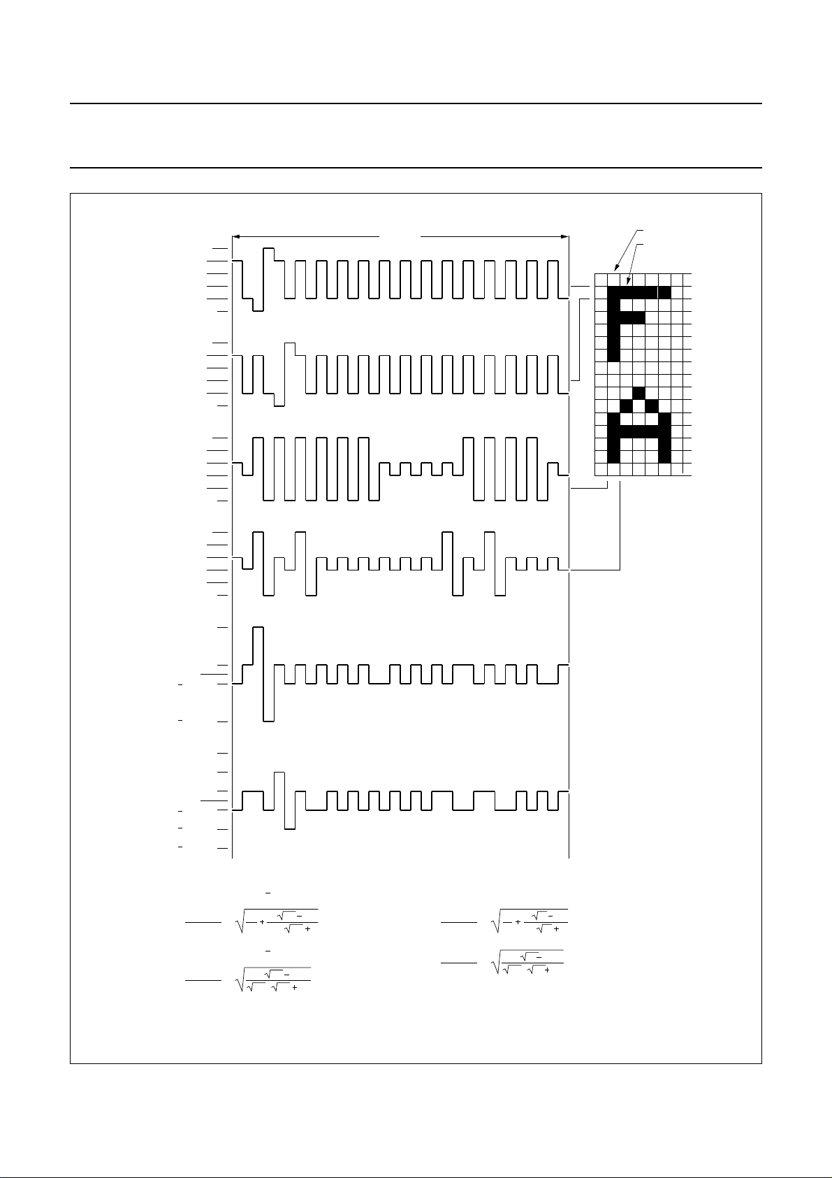
Fig.6 LCD row/column waveforms.
1998 Sep 08 11
Page 12
Philips Semiconductors Product specification
LCD row/column driver for dot matrix
graphic displays
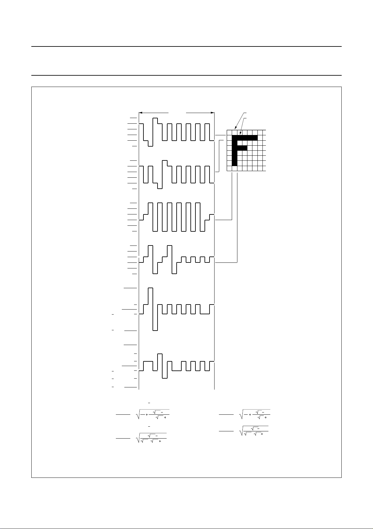
T
frame
ROW 1
R1 (t)
ROW 2
R2 (t)
COL 1
C1 (t)
V
V
V
V
V
V
V
V
V
V
V
V
V
V
V
V
V
V
DD
2
3
4
5
LCD
DD
2
3
4
5
LCD
DD
2
3
4
5
LCD
state 1 (OFF)
state 2 (ON)
dot matrix
1:8 multiplex rate
PCF8578
V
state 1
V
state 2
COL 2
C2 (t)
(t)
(t)
V
DD
V
2
V
3
V
4
V
5
V
LCD
V
op
0.261 V
0 V
0.261 V
V
op
V
op
0.478 V
0.261 V
0 V
0.261 V
0.478 V
V
op
V
state 1
V
on(rms)
V
op
V
state 2
V
off(rms)
V
op
op
op
op
op
op
op
(t) =C1(t) R1(t):
1
=
8
8
(t) = C2(t) R2(t):
()
8 1
2
=
()
8
8 1
=
8 1
=
0.297
2
0.430
()
8 1
MSA840
general relationship (n = multiplex rate)
V
on(rms)
V
op
V
off(rms)
V
op
=
=
1
n
()
n
n
n
()
n
1
2
()
n
n
1
1
1
2
Fig.7 LCD drive mode waveforms for 1 : 8 multiplex rate.
1998 Sep 08 12
Page 13
Philips Semiconductors Product specification
LCD row/column driver for dot matrix
graphic displays
T
frame
ROW 1
R1 (t)
ROW 2
R2 (t)
COL 1
C1 (t)
COL 2
C2 (t)
V
V
V
V
V
V
V
V
V
V
V
V
V
V
V
V
V
V
V
V
V
V
V
V
DD
2
3
4
5
LCD
DD
2
3
4
5
LCD
DD
2
3
4
5
LCD
DD
2
3
4
5
LCD
PCF8578
state 1 (OFF)
state 2 (ON)
dot matrix
1:16 multiplex rate
V
state 1
V
state 2
V
op
0.2 V
0 V
0.2 V
V
op
V
op
0.6 V
0.2 V
0 V
0.2 V
0.6 V
V
op
V
state 1
V
on(rms)
V
state 2
V
off(rms)
op
op
op
op
op
op
V
op
V
op
(t) = C1(t) R1(t):
1
16
16
16 1
()
=
(t) = C2(t) R2(t):
()
16 1
2
=
()
16 1
16
16 1
MSA836
general relationship (n = multiplex rate)
V
=
0.316
=
0.254
2
on(rms)
V
op
V
off(rms)
V
op
=
=
1
n
()
n
n
n
()
n
1
2
()
n
n
1
1
1
2
(t)
(t)
Fig.8 LCD drive mode waveforms for 1 : 16 multiplex rate.
1998 Sep 08 13
Page 14
Philips Semiconductors Product specification
LCD row/column driver for dot matrix
graphic displays
7.5 Internal clock
The clock signal for the system may be generated by the
internal oscillator and prescaler. The frequency is
determined by the value of the resistor R
For normal use a value of 330 kΩ is recommended.
The clock signal, for cascaded PCF8579s, is output at CLK
and has a frequency1⁄6 (multiplex rate 1 : 8, 1 : 16 and
1 : 32) or1⁄8 (multiplex rate 1 : 24) of the oscillator
frequency.
3
10
f
OSC
(kHz)
2
10
10
1
10
To avoid capacitive coupling, which could adversely affect oscillator
stability, R
pin. If this proves to be a problem, a filtering capacitor may be
connected in parallel to R
should be placed as closely as possible to the OSC
OSC
10
OSC
2
.
3
10
Fig.9 Oscillator frequency as a function of
external oscillator resistor, R
, see Fig.9.
OSC
MSA837
4
R(kΩ)
OSC
OSC
10
.
PCF8578
7.6 External clock
If an external clock is used, OSC must be connected to
VDD and the external clock signal to CLK. Table 4
summarizes the nominal CLK and SYNC frequencies.
7.7 Timing generator
The timing generator of the PCF8578 organizes the
internal data flow of the device and generates the LCD
frame synchronization pulse
integer multiple of the clock period. In cascaded
applications, this signal maintains the correct timing
relationship between the PCF8578 and PCF8579s in the
system.
7.8 Row/column drivers
Outputs R0 to R7 and C32 to C39 are fixed as row and
column drivers respectively. The remaining 24 outputs
R8/C8 to R31/C31 are programmable and may be
configured (in blocks of 8) to be either row or column
drivers. The row select signal is produced sequentially at
each output from R0 up to the number defined by the
multiplex rate (see Table 1). In mixed mode the remaining
outputs are configured as columns. In row mode all
programmable outputs (R8/C8 to R31/C31) are defined as
row drivers and the outputs C32 to C39 should be left
open-circuit.
Using a 1 : 16 multiplex rate, two sets of row outputs are
driven, thus facilitating split-screen configurations, i.e. a
row select pulse appears simultaneously at R0 and
R16/C16, R1 and R17/C17 etc. Similarly, using a multiplex
rate of 1 : 8, four sets of row outputs are driven
simultaneously. Driver outputs must be connected directly
to the LCD. Unused outputs should be left open-circuit.
In 1 : 8 R0 to R7 are rows; in 1 : 16 R0 to R15/C15 are
rows; in 1 : 24 R0 to R23/C23 are rows; in 1 : 32
R0 to R31/C31 are rows.
SYNC, whose period is an
Table 4 Signal frequencies required for nominal 64 Hz frame frequency; note 1.
OSCILLATOR
FREQUENCY
(2)
f
OSC
(Hz)
FRAME FREQUENCY
f
(Hz)
SYNC
MULTIPLEX RATE (n)
DIVISION
RATIO
12288 64 1 : 8, 1 : 16, 1 : 32 6 2048
12288 64 1 : 24 8 1536
Notes
1. A clock signal must always be present, otherwise the LCD may be frozen in a DC state.
2. R
OSC
= 330 kΩ.
1998 Sep 08 14
CLOCK FREQUENCY
f
(Hz)
CLK
Page 15

Philips Semiconductors Product specification
LCD row/column driver for dot matrix
graphic displays
7.9 Display mode controller
The configuration of the outputs (row or column) and the
selection of the appropriate driver waveforms are
controlled by the display mode controller.
7.10 Display RAM
The PCF8578 contains a 32 x 40-bit static RAM which
stores the display data. The RAM is divided into 4 banks
of 40 bytes (4 x 8 x 40 bits). During RAM access, data is
transferred to/from the RAM via the I
eight columns of data (0 to 7) cannot be displayed but
are available for general data storage and provide
compatibility with the PCF8579. There is a direct
correspondence between X-address and column output
number.
7.11 Data pointer
The addressing mechanism for the display RAM is
realized using the data pointer. This allows an individual
data byte or a series of data bytes to be written into, or read
from, the display RAM, controlled by commands sent on
2
C-bus.
the I
7.12 Subaddress counter
The storage and retrieval of display data is dependent on
the content of the subaddress counter. Storage takes
place only when the contents of the subaddress counter
agree with the hardware subaddress. The hardware
subaddress of the PCF8578, valid in mixed mode only, is
fixed at 0000.
7.13 I
The I2C-bus controller detects the I2C-bus protocol, slave
address, commands and display data bytes. It performs
the conversion of the data input (serial-to-parallel) and the
data output (parallel-to-serial). The PCF8578 acts as an
I2C-bus slave transmitter/receiver in mixed mode, and as
a slave receiver in row mode. A slave device cannot
control bus communication.
7.14 Input filters
To enhance noise immunity in electrically adverse
environments, RC low-pass filters are provided on the
SDA and SCL lines.
2
C-bus controller
2
C-bus. The first
PCF8578
7.15 RAM access
RAM operations are only possible when the PCF8578 is
in mixed mode.
In this event its hardware subaddress is internally fixed at
0000 and the hardware subaddresses of any PCF8579
used in conjunction with the PCF8578 must start at 0001.
There are three RAM ACCESS modes:
• Character
• Half-graphic
• Full-graphic.
These modes are specified by bits G1 to G0 of the RAM
ACCESS command. The RAM ACCESS command
controls the order in which data is written to or read from
the RAM (see Fig.10).
To store RAM data, the user specifies the location into
which the first byte will be loaded (see Fig.11):
• Device subaddress (specified by the DEVICE SELECT
command)
• RAM X-address (specified by the LOAD X-ADDRESS
command)
• RAM bank (specified by bits Y1 and Y0 of the RAM
ACCESS command).
Subsequent data bytes will be written or read according to
the chosen RAM ACCESS mode. Device subaddresses
are automatically incremented between devices until the
last device is reached. If the last device has
subaddress 15, further display data transfers will lead to a
wrap-around of the subaddress to 0.
7.16 Display control
The display is generated by continuously shifting rows of
RAM data to the dot matrix LCD via the column outputs.
The number of rows scanned depends on the multiplex
rate set by bits M1 and M0 of the SET MODE command.
The display status (all dots on/off and normal/inverse
video) is set by bits E1 and E0 of the SET MODE
command. For bank switching, the RAM bank
corresponding to the top of the display is set by bits
B1 and B0 of the SET START BANK command. This is
shown in Fig.12. This feature is useful when scrolling in
alphanumeric applications.
1998 Sep 08 15
7.17 TEST pin
The TEST pin must be connected to V
SS
.
Page 16

This text is here in white to force landscape pages to be rotated correctly when browsing through the pdf in the Acrobat reader.This text is here in
_white to force landscape pages to be rotated correctly when browsing through the pdf in the Acrobat reader.This text is here inThis text is here in
white to force landscape pages to be rotated correctly when browsing through the pdf in the Acrobat reader. white to force landscape pages to be ...
1998 Sep 08 16
PCF8578/PCF8579 PCF8579
Philips Semiconductors Product specification
LCD row/column driver for dot matrix
graphic displays
RAM
4 bytes
1 byte
2 bytes
driver 1
40-bits
01234567891011
0
246810121416182022
1357911131517192123
driver 2 driver k
PCF8578/PCF8579 system RAM
1 k 16
character mode
half-graphic mode
bank 0
bank 1
bank 2
bank 3
LSB
MSB
4 bytes
0
4 8 12 16 20 24 28 32 36 40 44
1 5 9 13 17 21 25 29 33 37 41 45
2 6 10 14 18 22 26 30 34 38 42 46
3 7 11 15 19 23 27 31 35 39 43 47
RAM data bytes are
written or read as
indicated above
full-graphic mode
Fig.10 RAM ACCESS mode.
MSA849
PCF8578
Page 17

This text is here in white to force landscape pages to be rotated correctly when browsing through the pdf in the Acrobat reader.This text is here in
_white to force landscape pages to be rotated correctly when browsing through the pdf in the Acrobat reader.This text is here inThis text is here in
white to force landscape pages to be rotated correctly when browsing through the pdf in the Acrobat reader. white to force landscape pages to be ...
1998 Sep 08 17
DEVICE SELECT:
subaddress 12
Philips Semiconductors Product specification
LCD row/column driver for dot matrix
graphic displays
RAM ACCESS:
character mode
bank 1
LOAD X-ADDRESS: X-address = 8
slave address
011110 0A
S
bank 0
bank 1
RAM
/RW
DEVICE SELECT
S
A
0
110110 A
1
LOAD X-ADDRESS
000100 A
1
0
0
last command
bank 2
bank 3
RAM ACCESS
111000 A
0
/RW
slave address
READ
1
WRITE
011110
S
DATA A DATA A
S
A
1A
0
DATA
A
MSA835
Fig.11 Example of commands specifying initial data byte RAM locations.
PCF8578
Page 18

Philips Semiconductors Product specification
LCD row/column driver for dot matrix
graphic displays
RAM
bank 0
bank 1
PCF8578
top of LCD
bank 2
bank 3
LCD
MSA851
Fig.12 Relationship between display and SET START BANK; 1 : 32 multiplex rate and start bank = 2.
1998 Sep 08 18
Page 19

Philips Semiconductors Product specification
LCD row/column driver for dot matrix
graphic displays
8I2C-BUS PROTOCOL
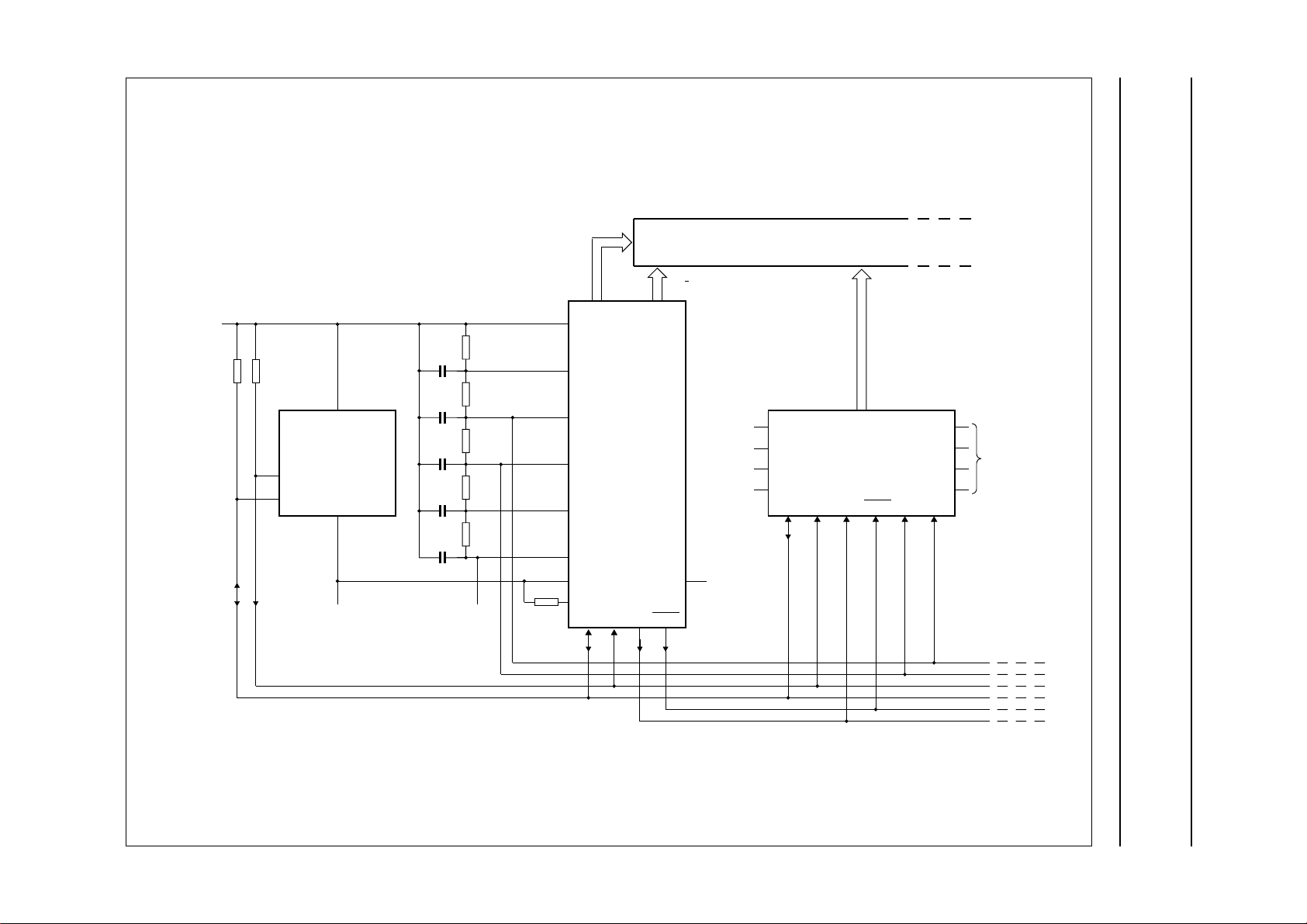
Two 7-bit slave addresses (0111100 and 0111101) are
reserved for both the PCF8578 and PCF8579. The least
significant bit of the slave address is set by connecting
input SA0 to either 0 (VSS) or 1 (VDD). Therefore, two types
of PCF8578 or PCF8579 can be distinguished on the
same I2C-bus which allows:
1. One PCF8578 to operate with up to 32 PCF8579s on
the same I2C-bus for very large applications
2. The use of two types of LCD multiplex schemes on the
same I2C-bus.
In most applications the PCF8578 will have the same slave
address as the PCF8579.
The I2C-bus protocol is shown in Fig.13.
All communications are initiated with a start condition (S)
from the I2C-bus master, which is followed by the desired
slave address and read/write bit. All devices with this slave
address acknowledge in parallel. All other devices ignore
the bus transfer.
In WRITE mode (indicated by setting the read/write bit
LOW) one or more commands follow the slave address
acknowledgement. The commands are also
acknowledged by all addressed devices on the bus.
The last command must clear the continuation bit C.
After the last command a series of data bytes may follow.
The acknowledgement after each byte is made only by the
(A0, A1, A2 and A3) addressed PCF8579 or PCF8578
with its implicit subaddress 0. After the last data byte
has been acknowledged, the I2C-bus master issues a stop
condition (P).
PCF8578
In READ mode, indicated by setting the read/write bit
HIGH, data bytes may be read from the RAM following the
slave address acknowledgement. After this
acknowledgement the master transmitter becomes a
master receiver and the PCF8578 becomes a slave
transmitter. The master receiver must acknowledge the
reception of each byte in turn. The master receiver must
signal an end of data to the slave transmitter, by not
generating an acknowledge on the last byte clocked out of
the slave. The slave transmitter then leaves the data line
HIGH, enabling the master to generate a stop condition
(P).
Display bytes are written into, or read from, the RAM at the
address specified by the data pointer and subaddress
counter. Both the data pointer and subaddress counter are
automatically incremented, enabling a stream of data to be
transferred either to, or from, the intended devices.
In multiple device applications, the hardware subaddress
pins of the PCF8579s (A0 to A3) are connected to V
VDD to represent the desired hardware subaddress code.
If two or more devices share the same slave address, then
each device must be allocated a unique hardware
subaddress.
SS
or
1998 Sep 08 19
Page 20

Philips Semiconductors Product specification
LCD row/column driver for dot matrix
graphic displays
acknowledge by
all addressed
PCF8578s / PCF8579s
/RW
slave address
S
A
0
acknowledge by
all addressed
PCF8578s / PCF8579s
A
011110 1A
S
COMMAND
slave address
slave address
S
011110 0AC
S
A
0
011110 0AC
S
COMMAND
(a)
PCF8578
acknowledge
by A0, A1, A2 and A3
selected PCF8578s /
PCF8579s only
A
n 0 byte(s)n 0 byte(s)1 byte
MSA830
acknowledge
from master
S
A
0
ADISPLAY DATA
P
update data pointers
and if necessary,
subaddress counter
no acknowledge
from master
ADATA
1DATA
P
/RW
S
MSA831
n 1 byte
PCF8578s / PCF8579s
slave address
011110 1A
at this moment master
transmitter becomes a
master receiver and
PCF8578/PCF8579 slave
receiver becomes a
slave transmitter
acknowledge by
all addressed
S
A
0
/RW
(b)
DATA
(c)
/RW
acknowledge
from master
A
n bytes last byte
no acknowledge
from master
1DATA
last byten bytes
update data pointers
and if necessary,
subaddress counter
update data pointers
and if necessary
subaddress counter
P
MSA832
Fig.13 (a) Master transmits to slave receiver (WRITE mode); (b) Master reads after sending command string
(WRITE commands; READ data); (c) Master reads slave immediately after sending slave address (READ
mode).
1998 Sep 08 20
Page 21

Philips Semiconductors Product specification
LCD row/column driver for dot matrix
PCF8578
graphic displays
8.1 Command decoder
The command decoder identifies command bytes that
arrive on the I2C-bus. The most-significant bit of a
command is the continuation bit C (see Fig.14). When this
bit is set, it indicates that the next byte to be transferred will
also be a command. If the bit is reset, it indicates the
conclusion of the command transfer. Further bytes will be
regarded as display data. Commands are transferred in
WRITE mode only.
C = 0; last command.
C = 1; commands continue.
The five commands available to the PCF8578 are defined
in Tables 5 and 6.
Table 5 Summary of commands
COMMAND OPCODE
(1)
SET MODE C 1 0 DDDDDmultiplex rate, display status, system type
SET START BANK C 11111DDdefines bank at top of LCD
DEVICE SELECT C 1 1 0 DDDDdefines device subaddress
RAM ACCESS C 1 1 1 DDDDgraphic mode, bank select (D D D D ≥ 12 is not
LOAD X-ADDRESS C 0 D DDDDD0to39
MSB LSB
C
REST OF OPCODE
MSA833
Fig.14 General information of command byte.
DESCRIPTION
allowed; see SET START BANK opcode)
Note
1. C = command continuation bit. D = may be a logic 1 or 0.
1998 Sep 08 21
Page 22

Philips Semiconductors Product specification
LCD row/column driver for dot matrix
PCF8578
graphic displays
Table 6 Definition of PCF8578/PCF8579 commands
COMMAND OPCODE OPTIONS DESCRIPTION
SET MODE C 1 0 T E1 E0 M1 M0 see Table 7 defines LCD drive mode
see Table 8 defines display status
see Table 9 defines system type
SET START BANK C 1 1 1 1 1 B1 B0 see Table 10 defines pointer to RAM bank
corresponding to the top of the LCD;
useful for scrolling, pseudo-motion and
background preparation of new display
DEVICE SELECT C 1 1 0 A3 A2 A1 A0 see Table 11 four bits of immediate data, bits
A0 to A3, are transferred to the
subaddress counter to define one of
sixteen hardware subaddresses
RAM ACCESS C 1 1 1 G1 G0 Y1 Y0 see T able 12 defines the auto-increment behaviour of
the address for RAM access
see Table 13 two bits of immediate data, bits Y0 to
Y1, are transferred to the X-address
pointer to define one of forty display
RAM columns
LOAD X-ADDRESS C 0 X5 X4 X3 X2 X1 X0 see Table 14 six bits of immediate data, bits
X0 to X5, are transferred to the
X-address pointer to define one of forty
display RAM columns
1998 Sep 08 22
Page 23

Philips Semiconductors Product specification
LCD row/column driver for dot matrix
graphic displays
Table 7 Set mode option 1
BITS
LCD DRIVE MODE
M1 M0
1 : 8 MUX ( 8 rows) 0 1
1 : 16 MUX (16 rows) 1 0
1 : 24 MUX (24 rows) 1 1
1 : 32 MUX (32 rows) 0 0
Table 8 Set mode option 2
BITS
DISPLAY STATUS
E1 E0
Blank 0 0
Normal 0 1
All segments on 1 0
Inverse video 1 1
Table 9 Set mode option 3
SYSTEM TYPE BIT T
PCF8578 row only 0
PCF8578 mixed mode 1
Table 10 Set start bank option 1
PCF8578
Table 11 Device select option 1
DESCRIPTION BITS
Decimal value 0 to 15 A3 A2 A1 A0
Table 12 RAM access option 1
BITS
RAM ACCESS MODE
G1 G0
Character 0 0
Half-graphic 0 1
Full-graphic 1 0
Not allowed (note 1) 1 1
Note
1. See opcode for SET START BANK in Table 6.
Table 13 Device select option 1
DESCRIPTION BITS
Decimal value 0 to 3 Y1 Y0
Table 14 Device select option 1
DESCRIPTION BITS
Decimal value 0 to 39 X5 X4 X3 X2 X1 X0
START BANK POINTER
Bank 0 0 0
Bank 1 0 1
Bank 2 1 0
Bank 3 1 1
BITS
B1 B0
1998 Sep 08 23
Page 24

Philips Semiconductors Product specification
LCD row/column driver for dot matrix
graphic displays
9 CHARACTERISTICS OF THE I2C-BUS
The I2C-bus is for bidirectional, two-line communication
between different ICs or modules. The two lines are a
serial data line (SDA) and a serial clock line (SCL) which
must be connected to a positive supply via a pull-up
resistor. Data transfer may be initiated only when the bus
is not busy.
9.1 Bit transfer
One data bit is transferred during each clock pulse.
The data on the SDA line must remain stable during the
HIGH period of the clock pulse as changes in the data line
at this moment will be interpreted as control signals.
9.2 Start and stop conditions
Both data and clock lines remain HIGH when the bus is not
busy. A HIGH-to-LOW transition of the data line, while the
clock is HIGH, is defined as the START condition (S).
A LOW-to-HIGH transition of the data line while the clock
is HIGH, is defined as the STOP condition (P).
PCF8578
9.4 Acknowledge
The number of data bytes transferred between the start
and stop conditions from transmitter to receiver is
unlimited. Each data byte of eight bits is followed by one
acknowledge bit. The acknowledge bit is a HIGH level put
on the bus by the transmitter, whereas the master
generates an extra acknowledge related clock pulse.
A slave receiver which is addressed must generate an
acknowledge after the reception of each byte. Also a
master must generate an acknowledge after the reception
of each byte that has been clocked out of the slave
transmitter. The device that acknowledges must pull down
the SDA line during the acknowledge clock pulse, so that
the SDA line is stable LOW during the HIGH period of the
acknowledge related clock pulse (set-up and hold times
must be taken into consideration). A master receiver must
signal the end of a data transmission to the transmitter by
not generating an acknowledge on the last byte that has
been clocked out of the slave. In this event the transmitter
must leave the data line HIGH to enable the master to
generate a stop condition.
9.3 System configuration
A device transmitting a message is a 'transmitter', a device
receiving a message is the 'receiver'. The device that
controls the message flow is the 'master' and the devices
which are controlled by the master are the 'slaves'.
SDA
SCL
data line
stable;
data valid
change
of data
allowed
MBA607
Fig.15 Bit transfer.
1998 Sep 08 24
Page 25

Philips Semiconductors Product specification
LCD row/column driver for dot matrix
graphic displays
SDA
SCL
S
START condition
Fig.16 Definition of start and stop condition.
P
STOP condition
PCF8578
SDA
SCL
MBA608
SDA
SCL
TRANSMITTER /
handbook, full pagewidth
BY TRANSMITTER
MASTER
RECEIVER
SCL FROM
MASTER
DATA OUTPUT
DATA OUTPUT
BY RECEIVER
START
condition
S
SLAVE
RECEIVER
SLAVE
TRANSMITTER /
RECEIVER
Fig.17 System configuration.
1
2
MASTER
TRANSMITTER
8
MBA606 - 1
MASTER
TRANSMITTER /
RECEIVER
clock pulse for
acknowledgement
9
MBA605
The general characteristics and detailed specification of the I2C-bus are available on request.
Fig.18 Acknowledgement on the I2C-bus.
1998 Sep 08 25
Page 26

Philips Semiconductors Product specification
LCD row/column driver for dot matrix
PCF8578
graphic displays
10 LIMITING VALUES
In accordance with the Absolute Maximum Rating System (IEC 134).
SYMBOL PARAMETER MIN. MAX. UNIT
V
V
V
V
V
V
I
I
I
P
P
T
I
O
DD
DD
LCD
I1
I2
o1
o2
, ISS, I
tot
o
stg
LCD
supply voltage −0.5 +8.0 V
LCD supply voltage VDD− 11 V
DD
input voltage SDA, SCL, CLK, TEST, SA0 and OSC VSS− 0.5 VDD+ 0.5 V
input voltage V2 to V
5
V
− 0.5 VDD+ 0.5 V
LCD
output voltage SYNC and CLK VSS− 0.5 VDD+ 0.5 V
output voltage R0 to R7, R8/C8 to R31/C31 and C32 to C39 V
− 0.5 VDD+ 0.5 V
LCD
DC input current −10 +10 mA
DC output current −10 +10 mA
VDD, VSS or V
current −50 +50 mA
LCD
total power dissipation per package − 400 mW
power dissipation per output − 100 mW
storage temperature −65 +150 °C
V
11 HANDLING
Inputs and outputs are protected against electrostatic discharge in normal handling. However, to be totally safe it is
desirable to take normal precautions appropriate to handling MOS devices. Advice can be found in Data Handbook IC12
under
“Handling MOS Devices”
.
1998 Sep 08 26
Page 27

Philips Semiconductors Product specification
LCD row/column driver for dot matrix
PCF8578
graphic displays
12 DC CHARACTERISTICS
V
= 2.5 to 6 V; VSS=0V;V
DD
LCD=VDD
SYMBOL PARAMETER CONDITIONS MIN. TYP. MAX. UNIT
Supplies
V
DD
V
LCD
I
DD1
I
DD2
V
POR
supply voltage 2.5 − 6.0 V
LCD supply voltage VDD− 9 − VDD− 3.5 V
supply current external clock f
supply current internal clock R
power-on reset level note 2 0.8 1.3 1.8 V
Logic
V
V
I
OL1
IL
IH
LOW level input voltage V
HIGH level input voltage 0.7V
LOW level output current at SYNC
and CLK
I
OH1
HIGH level output current at SYNC
and CLK
I
OL2
I
L1
LOW level output current at SDA VOL= 0.4 V; VDD=5V 3 −− mA
leakage current at SDA, SCL, SYNC,
CLK, TEST and SA0
I
L2
C
i
leakage current at OSC Vi=V
input capacitance at SCL and SDA note 3 −−5pF
LCD outputs
I
L3
V
DC
leakage current at V2 to V
DC component of LCD drivers
R0 to R7, R8/C8 to R31/C31 and
C32 to C39
R
ROW
output resistance R0 to R7 and
R8/C8 to R31/C31
R
COL
output resistance R8/C8 to R31/C31
and C32 to C39
− 3.5 V to VDD− 9V;T
= 2 kHz; note 1 − 615 µA
CLK
= 330 kΩ−20 50 µA
OSC
VOL=1V; VDD=5V 1 −− mA
VOH=4V; VDD=5V −−−1mA
Vi=VDD or V
DD
5
Vi=VDD or V
row mode; note 4 − 1.5 3 kΩ
column mode; note 4 − 36 kΩ
= −40 to +85 °C; unless otherwise specified.
amb
DD
− 0.3V
− V
DD
SS
SS
−−+1 mA
−−+1 µA
LCD
−2 − +2 µA
−±20 − mV
DD
V
V
Notes
1. Outputs are open; inputs at V
2. Resets all logic when VDD<V
or VSS; I2C-bus inactive; external clock with 50% duty factor.
DD
.
POR
3. Periodically sampled; not 100% tested.
4. Resistance measured between output terminal (R0 to R7, R8/C8 to R31/C31 and C32 to C39) and bias input
(V2to V5, VDD and V
) when the specified current flows through one output under the following conditions
LCD
(see Table 2):
a) Vop=VDD− V
b) Row mode, R0 to R7 and R8/C8 to R31/C31: V2− V
c) Column mode, R8/C8 to R31/C31 and C32 to C39: V3− V
LCD
=9V.
≥ 6.65 V; V5− V
LCD
≥ 4.70 V; V4− V
LCD
≤ 2.35 V; I
LCD
≤ 4.30 V; I
LCD
LOAD
= 150 µA.
= 100 µA.
LOAD
1998 Sep 08 27
Page 28

Philips Semiconductors Product specification
LCD row/column driver for dot matrix
PCF8578
graphic displays
13 AC CHARACTERISTICS
All timing values are referenced to V
V
= 2.5 to 6 V; VSS=0V; V
DD
LCD=VDD
SYMBOL PARAMETER CONDITIONS MIN. TYP. MAX. UNIT
f
CLK1
clock frequency at multiplex rates of
1 : 8, 1 : 16 and 1 : 32
f
CLK2
clock frequency at multiplex rates of
1:24
t
PSYNC
t
PLCD
2
C-bus
I
f
SCL
t
SW
t
BUF
t
SU;STA
t
HD;STA
t
LOW
t
HIGH
t
r
t
f
t
SU;DAT
t
HD;DAT
t
SU;STO
SYNC propagation delay −−500 ns
driver delays VDD− V
SCL clock frequency −−100 kHz
tolerable spike width on bus −−100 ns
bus free time 4.7 −−µs
start condition set-up time repeated start codes only 4.7 −−µs
start condition hold time 4.0 4.0 −µs
SCL LOW time 4.7 −−µs
SCL HIGH time 4.0 −−µs
SCL and SDA rise time −−1µs
SCL and SDA fall time −−0.3 µs
data set-up time 250 −−ns
data hold time 0 −−ns
stop condition set-up time 4.0 −−µs
and VIL levels with an input voltage swing of VSS to VDD.
IH
− 3.5 V to VDD− 9 V; T
R
OSC
R
OSC
= −40 to +85 °C; unless otherwise specified.
amb
= 330 kΩ; VDD= 6 V 1.2 2.1 3.3 kHz
= 330 kΩ; VDD= 6 V 0.9 1.6 2.5 kHz
LCD
=9V;
−−100 µs
with test loads
SYNC, CLK
C39 to C32,
R31/C31 to R8/C8
and R7 to R0
Ω3.3 k Ω1.5 k
0.5 V
DD
1 nF
Fig.19 AC test loads.
1998 Sep 08 28
SDA
V
MSA829
DD
Page 29

Philips Semiconductors Product specification
LCD row/column driver for dot matrix
graphic displays
1/ f
CLK
CLK
SYNC
t
PSYNC
C39 to C32,
R31/C31 to R8/C8
and R7 to R0
(V V = 9 V)
DD LCD
t
PLCD
t
PSYNC
MSA834
0.7 V
0.3 V
0.7 V
0.3 V
0.5 V
0.5 V
PCF8578
DD
DD
DD
DD
handbook, full pagewidth
SDA
SCL
SDA
MGA728
t
BUF
Fig.20 Driver timing waveforms.
t
LOW
t
HD;STA
t
r
t
SU;STA
t
HD;DAT
t
HIGH
t
f
t
SU;DAT
t
SU;STO
Fig.21 I2C-bus timing waveforms.
1998 Sep 08 29
Page 30

This text is here in white to force landscape pages to be rotated correctly when browsing through the pdf in the Acrobat reader.This text is here in
_white to force landscape pages to be rotated correctly when browsing through the pdf in the Acrobat reader.This text is here inThis text is here in
white to force landscape pages to be rotated correctly when browsing through the pdf in the Acrobat reader. white to force landscape pages to be ...
1998 Sep 08 30
LCD DISPLAY
R6R5R4R3R2R1R0
SDA
SCL
SYNC
CLK
R7
R8/C8R9/C9R10/
V
SA0
SS
TEST
OSC
V
DD
R11/
R12/
R13/
R14/
R15/
R16/
R17/
R18/
R19/
R20/
R21/
R22/
R23/
C10
C11
C12
C13
C14
C15
C16
C17
C18
C19
C20
C21
PCF8578
V
V3V
2
V
V
LCD
4
5
n.c.n.c.
C22
C23
C32
R24/
C24
R31/
C31
R25/
C25
R30/
C30
R26/
C26
R29/
C29
R27/
C27
R28/
C28C33C34C35C36C37C38C39
14 APPLICATION INFORMATION
Philips Semiconductors Product specification
LCD row/column driver for dot matrix
graphic displays
R
OSC
MSA844
PCF8578
Fig.22 Stand-alone application using 8 rows and 32 columns.
Page 31

This text is here in white to force landscape pages to be rotated correctly when browsing through the pdf in the Acrobat reader.This text is here in
_white to force landscape pages to be rotated correctly when browsing through the pdf in the Acrobat reader.This text is here inThis text is here in
white to force landscape pages to be rotated correctly when browsing through the pdf in the Acrobat reader. white to force landscape pages to be ...
1998 Sep 08 31
Philips Semiconductors Product specification
LCD row/column driver for dot matrix
graphic displays
R0
R7
R15
(Using 1:16 mux, the first
character data must be
loaded in bank 0 and 1
starting at byte number 16)
0
DISPLAY
RAM
PCF8578
R8
FREE RAM
a
f
b
g
e
c
dp
d
1
C16 C17 C39
16 17
ALTERNATE DISPLAY BANK
ALTERNATE DISPLAY BANK
1-byte
LCD
12
(1)
PCF8578: Segment Driver
Application
one line of 24 digits 7 segment
one line of 12 digits star-burst
(mux 1:16)
Total: 384 segments
39
Bank
0
1
2
3
MLB423
a
b
f
g
c
e
d
dp
LSB
MSB
(1) Can be used for creating blinking characters.
PCF8578
Fig.23 Segment driver application for up to 384 segments.
Page 32

This text is here in white to force landscape pages to be rotated correctly when browsing through the pdf in the Acrobat reader.This text is here in
_white to force landscape pages to be rotated correctly when browsing through the pdf in the Acrobat reader.This text is here inThis text is here in
white to force landscape pages to be rotated correctly when browsing through the pdf in the Acrobat reader. white to force landscape pages to be ...
1998 Sep 08 32
V
DD
V
R
C
R
C
(4 2 3)R
C
R
C
R
C
V
LCD
V
DD
DD
V
2
V
3
PCF8578
V
4
(ROW MODE)
V
5
V
LCD
V
SS
V
SS
SCLSDA
SA0
OSC
CLK SYNC
32
rows
8
unused columns
V
SS
R
OSC
V
SS
LCD DISPLAY
40
columns
V
V
DD
DD
V
LCD
V
3
V
4
V
SS
V
SS
1
PCF8579
CLKSYNC
SCL SDA SA0
A0
A1
A2
A3
V
SS
subaddress 0
V
V
DD
DD
V
LCD
V
3
V
4
V
SS
V
SS
2
PCF8579
CLKSYNC
SCL SDA SA0
40
columns
1:32 multiplex rate
32 x 40 x k dots (k 16)
(20480 dots max.)
subaddress 1
A0
A1
A2
A3
V
SS
V
40
columns
V
DD
DD
V
LCD
V
3
V
4
V
SS
V
SS
PCF8579
CLKSYNC
k
SCL SDA SA0
A0
A1
A2
A3
V
subaddress k 1
SS
Philips Semiconductors Product specification
LCD row/column driver for dot matrix
graphic displays
SCL
SDA
MSA845
PCF8578
Fig.24 Typical LCD driver system with 1 : 32 multiplex rate.
Page 33

This text is here in white to force landscape pages to be rotated correctly when browsing through the pdf in the Acrobat reader.This text is here in
_white to force landscape pages to be rotated correctly when browsing through the pdf in the Acrobat reader.This text is here inThis text is here in
white to force landscape pages to be rotated correctly when browsing through the pdf in the Acrobat reader. white to force landscape pages to be ...
1998 Sep 08 33
Philips Semiconductors Product specification
LCD row/column driver for dot matrix
graphic displays
V
SCL
SDA
V
DD
SCLSDASA0
A3
A2
PCF8579
A1
A0
SA0
OSC
subaddress k 1
16
rows
16
rows
8
unused columns
VSSV
/
DD
R
OSC
V
SS
V
V
DD
DD
V
LCD
PCF8579
V
3
V
4
V
CLKSYNC
SS
V
SS
V
DD
V
R
C
R
C
R
C
R
C
R
C
V
LCD
DD
DD
V
2
V
3
PCF8578
V
4
(ROW MODE)
V
5
V
LCD
V
SS
SCL
CLK SYNC
SDA
V
SS
SYNC
CLK
k
40
columns
LCD DISPLAY
40
columns
1
SCL
SDA SA0
V
V
V
LCD
V
V
SS
SS
V
3
V
4
DD
A0
A1
A2
A3
SS
V
DD
subaddress 1
subaddress 0
V
DD
SCLSDASA0
A3
A2
PCF8579
A1
A0
1:16 multiplex rate
16 x 40 x k dots (k 16)
(10240 dots max.)
1:16 multiplex rate
16 x 40 x k dots (k 16)
(10240 dots max.)
V
V
DD
DD
V
LCD
PCF8579
V
3
V
4
V
CLKSYNC
SS
V
SS
CLK
2
40
columns
40
columns
2
SCL
SYNC
SDA SA0
V
V
V
LCD
V
SS
SS
V
3
V
4
DD
A0
A1
A2
A3
V
SS
V
DD
subaddress 0
subaddress 1
V
DD
SCLSDASA0
A3
A2
PCF8579
A1
A0
V
V
DD
DD
V
LCD
PCF8579
V
3
V
4
V
CLKSYNC
SS
V
SS
CLK
1
40
columns
40
columns
k
SCL
SYNC
SDA SA0
V
SS
V
SS
V
3
V
4
V
LCD
V
DD
subaddress k 1
A0
A1
A2
A3
V
SS
V
DD
MSA847
Fig.25 Split screen application with 1 : 16 multiplex rate for improved contrast.
PCF8578
Page 34

This text is here in white to force landscape pages to be rotated correctly when browsing through the pdf in the Acrobat reader.This text is here in
_white to force landscape pages to be rotated correctly when browsing through the pdf in the Acrobat reader.This text is here inThis text is here in
white to force landscape pages to be rotated correctly when browsing through the pdf in the Acrobat reader. white to force landscape pages to be ...
1998 Sep 08 34
Philips Semiconductors Product specification
LCD row/column driver for dot matrix
graphic displays
V
SCL
SDA
V
DD
SCLSDASA0
A3
A2
PCF8579
A1
A0
SA0
OSC
subaddress k 1
32
rows
8
unused columns
VSSV
/
DD
R
OSC
V
SS
V
V
DD
DD
V
LCD
PCF8579
V
3
V
4
V
CLKSYNC
SS
V
SS
V
DD
V
R
C
(4 2 3)R
R
C
C
R
C
R
C
V
LCD
DD
DD
V
2
V
3
PCF8578
V
4
(ROW MODE)
V
5
V
LCD
V
SS
SCL
CLK SYNC
SDA
V
SS
SYNC
CLK
k
40
columns
LCD DISPLAY
40
columns
1
SCL
SDA SA0
V
V
V
LCD
V
V
SS
SS
V
3
V
4
DD
A0
A1
A2
A3
SS
V
DD
subaddress 1
subaddress 0
V
DD
SCLSDASA0
A3
A2
PCF8579
A1
A0
1:32 multiplex rate
32 x 40 x k dots (k 16)
(20480 dots max.)
1:32 multiplex rate
32 x 40 x k dots (k 16)
(20480 dots max.)
V
V
DD
DD
V
LCD
PCF8579
V
3
V
4
V
CLKSYNC
SS
V
SS
CLK
2
40
columns
40
columns
2
SCL
SYNC
SDA SA0
V
V
V
LCD
V
SS
SS
V
3
V
4
DD
A0
A1
A2
A3
V
SS
V
DD
subaddress 0
subaddress 1
V
DD
SCLSDASA0
A3
A2
PCF8579
A1
A0
V
V
DD
DD
V
LCD
PCF8579
V
3
V
4
V
CLKSYNC
SS
V
SS
CLK
1
40
columns
40
columns
k
SCL
SYNC
SDA SA0
V
SS
V
SS
V
3
V
4
V
LCD
V
DD
subaddress k 1
A0
A1
A2
A3
V
SS
V
DD
32
MSA846
PCF8578
Fig.26 Split screen application with 1 : 32 multiplex rate.
Page 35

This text is here in white to force landscape pages to be rotated correctly when browsing through the pdf in the Acrobat reader.This text is here in
_white to force landscape pages to be rotated correctly when browsing through the pdf in the Acrobat reader.This text is here inThis text is here in
white to force landscape pages to be rotated correctly when browsing through the pdf in the Acrobat reader. white to force landscape pages to be ...
1998 Sep 08 35
V
SS
V
SCL
DD
V
(4 2 3)R
SDA
R
OSC
RRRR
n.c.
n.c.
PCF8578
LCD
R0
LCD DISPLAY
Philips Semiconductors Product specification
LCD row/column driver for dot matrix
graphic displays
R31/C31
C0 C27 C28 C39
PCF8579
n.c.
C0 C27 C28 C39
PCF8579
n.c.
Fig.27 Example of single plane wiring, single screen with 1 : 32 multiplex rate (PCF8578 in row driver mode).
MSA852
to other
PCF8579s
PCF8578
Page 36

Philips Semiconductors Product specification
LCD row/column driver for dot matrix
graphic displays
15 CHIP DIMENSIONS AND BONDING PAD LOCATIONS
SS
CLK
V
4.88
mm
V
OSC
V
DD
V
V
V
V
LCD
C39
C38
C37
C36
C35
TEST
SA0
7
8
9
10
2
11
3
12
4
13
5
14
15
16
17
18
19
SYNC
0
PCF8578
y
R0
SCL
SDA
123456 53 52 51 50
0
R1
54
R2
R3
PCF8578
R4
49
R5
48
R6
47
R7
46
R8/C8
R9/C9
45
R10/C10
44
43
R11/C11
42
R12/C12
41
R13/C13
R14/C14
40
39
R15/C15
R16/C16
38
R17/C17
37
36
R18/C18
35
R19/C19
R20/C20
34
R21/C21
33
R22/C22
32
x
C34
C33
C32
R31/C31
R30/C30
3.06 mm
Chip area: 14.93 mm2.
Bonding pad dimensions: 120 µm × 120 µm.
The numbers given in the small squares refer to the pad numbers.
Fig.28 Bonding pad locations.
1998 Sep 08 36
R29/C29
R28/C28
R27/C27
R26/C26
R25/C25
R24/C24
313029282726252423222120
R23/C23
MBH589
Page 37

Philips Semiconductors Product specification
LCD row/column driver for dot matrix
graphic displays
Table 15 Bonding pad locations (dimensions in µm)
All x/y coordinates are referenced to centre of chip, see Fig.28.
PAD NUMBER SYMBOL x y
1 SDA 174 2241 1 7
2 SCL −30 2241 2 8
3
4 CLK −468 2241 4 10
5V
6 TEST −1014 2241 6 12
7 SA0 −1308 2241 7 13
8 OSC −1308 1917 8 16
9V
10 V
11 V
12 V
13 V
14 V
15 C39 −1308 −1149 17 29
16 C38 −1308 −1353 18 30
17 C37 −1308 −1557 19 31
18 C36 −1308 −1773 20 32
19 C35 −1308 −1995 21 33
20 C34 −1308 −2241 22 34
21 C33 −1014 −2241 23 35
22 C32 −726 −2241 24 37
23 R31/C31 −468 −2241 25 38
24 R30/C30 −234 −2241 26 39
25 R29/C29 −30 −2241 27 40
26 R28/C28 174 −2241 28 41
27 R27/C27 468 −2241 29 42
28 R26/C26 672 −2241 30 43
29 R25/C25 876 −2241 31 44
30 R24/C24 1080 −2241 32 45
31 R23/C23 1308 −2241 33 46
32 R22/C22 1308 −1977 34 48
33 R21/C21 1308 −1731 35 49
34 R20/C20 1308 −1515 36 50
35 R19/C19 1308 −1305 37 51
36 R18/C18 1308 −1101 38 52
37 R17/C17 1308 −897 39 53
SYNC −234 2241 3 9
SS
DD
2
3
4
5
LCD
−726 2241 5 11
−1308 1113 9 20
−1308 873 10 21
−1308 663 11 22
−1308 459 12 23
−1308 255 13 24
−1308 51 14 25
PCF8578
PINS
VSO56 LQFP64
1998 Sep 08 37
Page 38

Philips Semiconductors Product specification
LCD row/column driver for dot matrix
graphic displays
PINS
PAD NUMBER SYMBOL x y
VSO56 LQFP64
38 R16/C16 1308 −693 40 54
39 R15/C15 1308 −489 41 55
40 R14/C14 1308 −285 42 56
41 R13/C13 1308 −81 43 57
42 R12/C12 1308 123 44 58
43 R11/C11 1308 351 45 59
44 R10/C10 1308 603 46 60
45 R9/C9 1308 1101 47 61
46 R8/C8 1308 1305 48 62
47 R7 1308 1515 49 63
48 R6 1308 1731 50 64
49 R5 1308 1977 51 1
50 R4 1308 2241 52 2
51 R3 1080 2241 53 3
52 R2 876 2241 54 4
53 R1 672 2241 55 5
54 R0 468 2241 56 6
− n.c. −−15, 16 14, 15, 17 to 19,
PCF8578
26 to 28, 36, 47
1998 Sep 08 38
Page 39

This text is here in white to force landscape pages to be rotated correctly when browsing through the pdf in the Acrobat reader.This text is here in
_white to force landscape pages to be rotated correctly when browsing through the pdf in the Acrobat reader.This text is here inThis text is here in
white to force landscape pages to be rotated correctly when browsing through the pdf in the Acrobat reader. white to force landscape pages to be ...
1998 Sep 08 39
V
DD
V
3
V
4
V
LCD
V
SS
CLK
SYNC
SCL
SDA
R0
R1
R2
SDA
SCL
R
SYNC
CLK
OSC
SA0
OSC
TEST
V
SS
DD
V
2
V
3
V
4
V
5
V
LCD
V
C0
C1
C39
C38
SDA
SCL
SYNC
CLK
V
SS
TEST
SA0
A3
A2
A1
A0
DD
V
n.c.
3
V
4
V
LCD
V
V
DD
V
V
V
V
CLK
SYNC
SCL
SDA
3
4
LCD
SS
16 CHIP-ON GLASS INFORMATION
Philips Semiconductors Product specification
LCD row/column driver for dot matrix
graphic displays
PCF8578
R0 to R31
C0 C1 C2
If inputs SA0 and A0 to A3 are left unconnected they are internally pulled to VDD.
Fig.29 Typical chip-on glass application (viewed from the underside of the chip).
LCD
DISPLAY
PCF8579
C39
C38
C37
PCF8578
MSA850
Page 40

Philips Semiconductors Product specification
LCD row/column driver for dot matrix
graphic displays
17 PACKAGE OUTLINES
VSO56: plastic very small outline package; 56 leads
D
y
Z
56
PCF8578
SOT190-1
E
c
H
E
29
A
X
v M
A
pin 1 index
281
w M
b
e
0 5 10 mm
DIMENSIONS (inch dimensions are derived from the original mm dimensions)
mm
A
max.
3.3
0.13
0.3
0.1
0.012
0.004
3.0
2.8
0.12
0.11
2
A3b
0.25
0.01
p
0.42
0.30
0.017
0.012
0.22
0.14
0.0087
0.0055
UNIT A1A
inches
Note
1. Plastic or metal protrusions of 0.3 mm maximum per side are not included.
2. Plastic interlead protrusions of 0.25 mm maximum per side are not included.
(1)E(2)
cD
21.65
21.35
0.85
0.84
p
scale
eHELLpQZywv θ
11.1
0.75
11.0
0.44
0.0295
0.43
15.8
15.2
0.62
0.60
2.25
0.089
Q
A
2
A
1
1.6
1.4
0.063
0.055
detail X
1.45
0.2
1.30
0.057
0.008 0.004
0.051
L
p
L
0.1 0.1
0.004
(A )
A
3
θ
(1)
0.90
0.55
0.035
0.022
o
7
o
0
OUTLINE
VERSION
SOT190-1
IEC JEDEC EIAJ
REFERENCES
1998 Sep 08 40
EUROPEAN
PROJECTION
ISSUE DATE
96-04-02
97-08-11
Page 41

Philips Semiconductors Product specification
LCD row/column driver for dot matrix
graphic displays
LQFP64: plastic low profile quad flat package; 64 leads; body 10 x 10 x 1.4 mm
c
y
X
A
48 33
49
Z
32
E
PCF8578
SOT314-2
e
w M
b
p
e
pin 1 index
1.45
1.35
b
0.25
17
16
Z
w M
p
D
H
D
p
0.27
0.18
0.17
0.12
D
(1)
(1) (1)(1)
cE
D
10.1
10.1
9.9
9.9
v M
B
v M
B
0 2.5 5 mm
scale
eH
H
D
12.15
0.5
11.85
64
1
DIMENSIONS (mm are the original dimensions)
mm
A
A1A2A3b
max.
0.20
1.60
0.05
UNIT
Note
1. Plastic or metal protrusions of 0.25 mm maximum per side are not included.
E
A
H
12.15
11.85
E
LL
E
A
2
A
A
1
detail X
Z
1.45
1.05
D
0.75
0.45
p
0.12 0.11.0 0.2
(A )
3
L
p
L
Zywv θ
E
1.45
1.05
o
7
o
0
θ
OUTLINE
VERSION
SOT314-2
IEC JEDEC EIAJ
REFERENCES
1998 Sep 08 41
EUROPEAN
PROJECTION
ISSUE DATE
95-12-19
97-08-01
Page 42

Philips Semiconductors Product specification
LCD row/column driver for dot matrix
graphic displays
18 SOLDERING
18.1 Introduction
There is no soldering method that is ideal for all IC
packages. Wave soldering is often preferred when
through-hole and surface mounted components are mixed
on one printed-circuit board. However, wave soldering is
not always suitable for surface mounted ICs, or for
printed-circuits with high population densities. In these
situations reflow soldering is often used.
This text gives a very brief insight to a complex technology.
A more in-depth account of soldering ICs can be found in
our
“Data Handbook IC26; Integrated Circuit Packages”
(order code 9398 652 90011).
18.2 Reflow soldering
Reflow soldering techniques are suitable for all LQFP and
VSO packages.
Reflow soldering requires solder paste (a suspension of
fine solder particles, flux and binding agent) to be applied
to the printed-circuit board by screen printing, stencilling or
pressure-syringe dispensing before package placement.
Several methods exist for reflowing; for example,
infrared/convection heating in a conveyor type oven.
Throughput times (preheating, soldering and cooling) vary
between 50 and 300 seconds depending on heating
method. Typical reflow peak temperatures range from
215 to 250 °C.
18.3 Wave soldering
18.3.1 LQFP
Wave soldering is not recommended for LQFP packages.
This is because of the likelihood of solder bridging due to
closely-spaced leads and the possibility of incomplete
solder penetration in multi-lead devices.
PCF8578
If wave soldering cannot be avoided, for LQFP
packages with a pitch (e) larger than 0.5 mm, the
following conditions must be observed:
• A double-wave (a turbulent wave with high upward
pressure followed by a smooth laminar wave)
soldering technique should be used.
• The footprint must be at an angle of 45° to the board
direction and must incorporate solder thieves
downstream and at the side corners.
18.3.2 VSO
Wave soldering techniques can be used for all VSO
packages if the following conditions are observed:
• A double-wave (a turbulent wave with high upward
pressure followed by a smooth laminar wave) soldering
technique should be used.
• The longitudinal axis of the package footprint must be
parallel to the solder flow.
• The package footprint must incorporate solder thieves at
the downstream end.
18.3.3 M
During placement and before soldering, the package must
be fixed with a droplet of adhesive. The adhesive can be
applied by screen printing, pin transfer or syringe
dispensing. The package can be soldered after the
adhesive is cured.
Maximum permissible solder temperature is 260 °C, and
maximum duration of package immersion in solder is
10 seconds, if cooled to less than 150 °C within
6 seconds. Typical dwell time is 4 seconds at 250 °C.
A mildly-activated flux will eliminate the need for removal
of corrosive residues in most applications.
18.4 Repairing soldered joints
ETHOD (LQFP AND VSO)
CAUTION
Wave soldering is NOT applicable for all LQFP
packages with a pitch (e) equal or less than 0.5 mm.
1998 Sep 08 42
Fix the component by first soldering two diagonallyopposite end leads. Use only a low voltage soldering iron
(less than 24 V) applied to the flat part of the lead. Contact
time must be limited to 10 seconds at up to 300 °C. When
using a dedicated tool, all other leads can be soldered in
one operation within 2 to 5 seconds between
270 and 320 °C.
Page 43

Philips Semiconductors Product specification
LCD row/column driver for dot matrix
PCF8578
graphic displays
19 DEFINITIONS
Data sheet status
Objective specification This data sheet contains target or goal specifications for product development.
Preliminary specification This data sheet contains preliminary data; supplementary data may be published later.
Product specification This data sheet contains final product specifications.
Limiting values
Limiting values given are in accordance with the Absolute Maximum Rating System (IEC 134). Stress above one or
more of the limiting values may cause permanent damage to the device. These are stress ratings only and operation
of the device at these or at any other conditions above those given in the Characteristics sections of this specification
is not implied. Exposure to limiting values for extended periods may affect device reliability.
Application information
Where application information is given, it is advisory and does not form part of the specification.
20 LIFE SUPPORT APPLICATIONS
These products are not designed for use in life support appliances, devices, or systems where malfunction of these
products can reasonably be expected to result in personal injury. Philips customers using or selling these products for
use in such applications do so at their own risk and agree to fully indemnify Philips for any damages resulting from such
improper use or sale.
21 PURCHASE OF PHILIPS I
Purchase of Philips I
components in the I2C system provided the system conforms to the I2C specification defined by
Philips. This specification can be ordered using the code 9398 393 40011.
2
C COMPONENTS
2
C components conveys a license under the Philips’ I2C patent to use the
1998 Sep 08 43
Page 44

Philips Semiconductors – a worldwide company
Argentina: see South America
Australia: 34 Waterloo Road, NORTH RYDE, NSW 2113,
Tel. +61 2 9805 4455, Fax. +61 2 9805 4466
Austria: Computerstr. 6, A-1101 WIEN, P.O. Box 213, Tel. +43 160 1010,
Fax. +43 160 101 1210
Belarus: Hotel Minsk Business Center, Bld. 3, r. 1211, Volodarski Str. 6,
220050 MINSK, Tel. +375 172 200 733, Fax. +375 172 200 773
Belgium: see The Netherlands
Brazil: see South America
Bulgaria: Philips Bulgaria Ltd., Energoproject, 15th floor,
51 James Bourchier Blvd., 1407 SOFIA,
Tel. +359 2 689 211, Fax. +359 2 689 102
Canada: PHILIPS SEMICONDUCTORS/COMPONENTS,
Tel. +1 800 234 7381
China/Hong Kong: 501 Hong Kong Industrial Technology Centre,
72 Tat Chee Avenue, Kowloon Tong, HONG KONG,
Tel. +852 2319 7888, Fax. +852 2319 7700
Colombia: see South America
Czech Republic: see Austria
Denmark: Prags Boulevard 80, PB 1919, DK-2300 COPENHAGEN S,
Tel. +45 32 88 2636, Fax. +45 31 57 0044
Finland: Sinikalliontie 3, FIN-02630 ESPOO,
Tel. +358 9 615800, Fax. +358 9 61580920
France: 51 Rue Carnot, BP317, 92156 SURESNES Cedex,
Tel. +33 1 40 99 6161, Fax. +33 1 40 99 6427
Germany: Hammerbrookstraße 69, D-20097 HAMBURG,
Tel. +49 40 23 53 60, Fax. +49 40 23 536 300
Greece: No. 15, 25th March Street, GR 17778 TAVROS/ATHENS,
Tel. +30 1 4894 339/239, Fax. +30 1 4814 240
Hungary: see Austria
India: Philips INDIA Ltd, Band Box Building, 2nd floor,
254-D, Dr. Annie Besant Road, Worli, MUMBAI 400 025,
Tel. +91 22 493 8541, Fax. +91 22 493 0966
Indonesia: PT Philips Development Corporation, Semiconductors Division,
Gedung Philips, Jl. Buncit Raya Kav.99-100, JAKARTA 12510,
Tel. +62 21 794 0040 ext. 2501, Fax. +62 21 794 0080
Ireland: Newstead, Clonskeagh, DUBLIN 14,
Tel. +353 1 7640 000, Fax. +353 1 7640 200
Israel: RAPAC Electronics, 7 Kehilat Saloniki St, PO Box 18053,
TEL AVIV 61180, Tel. +972 3 645 0444, Fax. +972 3 649 1007
Italy: PHILIPS SEMICONDUCTORS, Piazza IV Novembre 3,
20124 MILANO, Tel. +39 2 6752 2531, Fax. +39 2 6752 2557
Japan: Philips Bldg 13-37, Kohnan 2-chome, Minato-ku,
TOKYO 108-8507, Tel. +81 3 3740 5130, Fax. +81 3 3740 5077
Korea: Philips House, 260-199 Itaewon-dong, Yongsan-ku, SEOUL,
Tel. +82 2 709 1412, Fax. +82 2 709 1415
Malaysia: No. 76 Jalan Universiti, 46200 PETALING JAYA, SELANGOR,
Tel. +60 3 750 5214, Fax. +60 3 757 4880
Mexico: 5900 Gateway East, Suite 200, EL PASO, TEXAS 79905,
Tel. +9-5 800 234 7381
Middle East: see Italy
Netherlands: Postbus 90050, 5600 PB EINDHOVEN, Bldg. VB,
Tel. +31 40 27 82785, Fax. +31 40 27 88399
New Zealand: 2 Wagener Place, C.P.O. Box 1041, AUCKLAND,
Tel. +64 9 849 4160, Fax. +64 9 849 7811
Norway: Box 1, Manglerud 0612, OSLO,
Tel. +47 22 74 8000, Fax. +47 22 74 8341
Pakistan: see Singapore
Philippines: Philips Semiconductors Philippines Inc.,
106 Valero St. Salcedo Village, P.O. Box 2108 MCC, MAKATI,
Metro MANILA, Tel. +63 2 816 6380, Fax. +63 2 817 3474
Poland: Ul. Lukiska 10, PL 04-123 WARSZAWA,
Tel. +48 22 612 2831, Fax. +48 22 612 2327
Portugal: see Spain
Romania: see Italy
Russia: Philips Russia, Ul. Usatcheva 35A, 119048 MOSCOW,
Tel. +7 095 755 6918, Fax. +7 095 755 6919
Singapore: Lorong 1, Toa Payoh, SINGAPORE 319762,
Tel. +65 350 2538, Fax. +65 251 6500
Slovakia: see Austria
Slovenia: see Italy
South Africa: S.A. PHILIPS Pty Ltd., 195-215 Main Road Martindale,
2092 JOHANNESBURG, P.O. Box 7430 Johannesburg 2000,
Tel. +27 11 470 5911, Fax. +27 11 470 5494
South America: Al. Vicente Pinzon, 173, 6th floor,
04547-130 SÃO PAULO, SP, Brazil,
Tel. +55 11 821 2333, Fax. +55 11 821 2382
Spain: Balmes 22, 08007 BARCELONA,
Tel. +34 93 301 6312, Fax. +34 93 301 4107
Sweden: Kottbygatan 7, Akalla, S-16485 STOCKHOLM,
Tel. +46 8 5985 2000, Fax. +46 8 5985 2745
Switzerland: Allmendstrasse 140, CH-8027 ZÜRICH,
Tel. +41 1 488 2741 Fax. +41 1 488 3263
Taiwan: Philips Semiconductors, 6F, No. 96, Chien Kuo N. Rd., Sec. 1,
TAIPEI, Taiwan Tel. +886 2 2134 2865, Fax. +886 2 2134 2874
Thailand: PHILIPS ELECTRONICS (THAILAND) Ltd.,
209/2 Sanpavuth-Bangna Road Prakanong, BANGKOK 10260,
Tel. +66 2 745 4090, Fax. +66 2 398 0793
Turkey: Talatpasa Cad. No. 5, 80640 GÜLTEPE/ISTANBUL,
Tel. +90 212 279 2770, Fax. +90 212 282 6707
Ukraine: PHILIPS UKRAINE, 4 Patrice Lumumba str., Building B, Floor 7,
252042 KIEV, Tel. +380 44 264 2776, Fax. +380 44 268 0461
United Kingdom: Philips Semiconductors Ltd., 276 Bath Road, Hayes,
MIDDLESEX UB3 5BX, Tel. +44 181 730 5000, Fax. +44 181 754 8421
United States: 811 East Arques Avenue, SUNNYVALE, CA 94088-3409,
Tel. +1 800 234 7381
Uruguay: see South America
Vietnam: see Singapore
Yugoslavia: PHILIPS, Trg N. Pasica 5/v, 11000 BEOGRAD,
Tel. +381 11 625 344, Fax.+381 11 635 777
For all other countries apply to: Philips Semiconductors,
International Marketing & Sales Communications, Building BE-p, P.O. Box 218,
5600 MD EINDHOVEN, The Netherlands, Fax. +31 40 27 24825
© Philips Electronics N.V. 1998 SCA60
All rights are reserved. Reproduction in whole or in part is prohibited without the prior written consent of the copyright owner.
The information presented in this document does not form part of any quotation or contract, is believed to be accurate and reliable and may be changed
without notice. No liability will be accepted by the publisher for any consequence of its use. Publication thereof does not convey nor imply any license
under patent- or other industrial or intellectual property rights.
Internet: http://www.semiconductors.philips.com
Printed in The Netherlands 415106/750/04/pp44 Date of release: 1998 Sep 08 Document order number: 9397 75004312
 Loading...