

Page 1

PCF8563
Real-time clock/calendar
16 April 1999 Product specification
1. General description
The PCF8563 is a CMOS real-time clock/calendar optimized for low power
consumption. A programmableclockoutput,interruptoutputandvoltage-low detector
are also provided. All address and data are transferred serially via a two-line
bidirectional I2C-bus. Maximum bus speed is 400 kbits/s. The built-in word address
register is incremented automatically after each written or read data byte.
2. Features
■ Provides year, month, day, weekday, hours, minutes and seconds based on
32.768 kHz quartz crystal
■ Century flag
■ Wide operating supply voltage range: 1.0 to 5.5 V
■ Low back-up current; typical 0.25 µA at VDD= 3.0 V and T
■ 400 kHz two-wire I2C-bus interface (at VDD= 1.8 to 5.5 V)
■ Programmable clock output for peripheral devices: 32.768 kHz, 1024 Hz,
32 Hz and 1 Hz
■ Alarm and timer functions
■ Voltage-low detector
■ Integrated oscillator capacitor
■ Internal power-on reset
■ I2C-bus slave address: read A3H; write A2H
■ Open drain interrupt pin.
amb
=25°C
3. Applications
■ Mobile telephones
■ Portable instruments
■ Fax machines
■ Battery powered products.
Page 2
Philips Semiconductors
PCF8563
Real-time clock/calendar
4. Quick reference data
Table 1: Quick reference data
Symbol Parameter Conditions Min Max Unit
V
DD
I
DD
T
amb
T
stg
supply voltage operating mode I2C-bus inactive; T
2
C-bus active; f
I
= −40 to +85 °C
T
amb
supply current; timer and CLKOUT
disabled
f
= 400 kHz - 800 µA
SCL
= 100 kHz - 200 µA
f
SCL
= 0 Hz; T
f
SCL
V
V
DD
DD
amb
= 5 V - 550 nA
= 2 V - 450 nA
operating ambient temperature −40 +85 °C
storage temperature −65 +150 °C
=25°C 1.0 5.5 V
amb
= 400 kHz;
SCL
1.8 5.5 V
=25°C
5. Ordering information
Table 2: Ordering information
Type number Package
Name Description Version
PCF8563P DIP8 plastic dual in-line package; 8 leads (300 mil) SOT97-1
PCF8563T SO8 plastic small outline package; 8 leads; body width 3.9 mm SOT96-1
PCF8563TS TSSOP8 plastic thin shrink small outline package; 8 leads; body width 3.0 mm SOT505-1
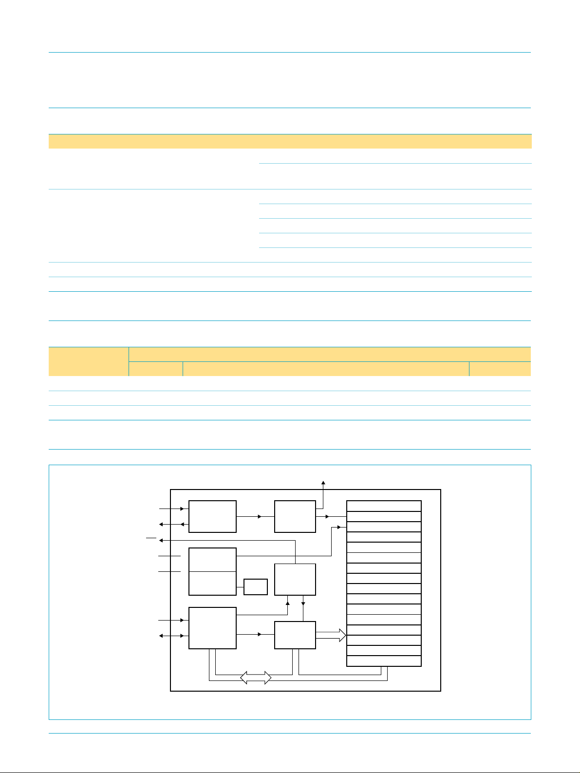
6. Block diagram
DIVIDER
LOGIC
CLKOUT
7
CONTROL/STATUS 1
1 Hz
CONTROL/STATUS 2
SECONDS/VL
MINUTES
HOURS
DAYS
WEEKDAYS
MONTHS/CENTURY
YEARS
MINUTE ALARM
HOUR ALARM
DAY ALARM
WEEKDAY ALARM
CLKOUT CONTROL
TIMER CONTROL
TIMER
0
1
2
3
4
5
6
7
8
9
A
B
C
D
E
F
handbook, full pagewidth
OSCI
OSCO
INT
V
SS
V
DD
SCL
SDA
1
2
3
4
8
6
5
OSCILLATOR
32.768 kHz
VOLTAGE
DETECTOR
OSCILLATOR
MONITOR
I2C-BUS
INTERFACE
POR
CONTROL
ADDRESS
REGISTER
MGM662
Fig 1. Block diagram.
9397 750 04855
Product specification 16 April 1999 2 of 30
© Philips Electronics N.V. 1999. All rights reserved.
Page 3
Philips Semiconductors
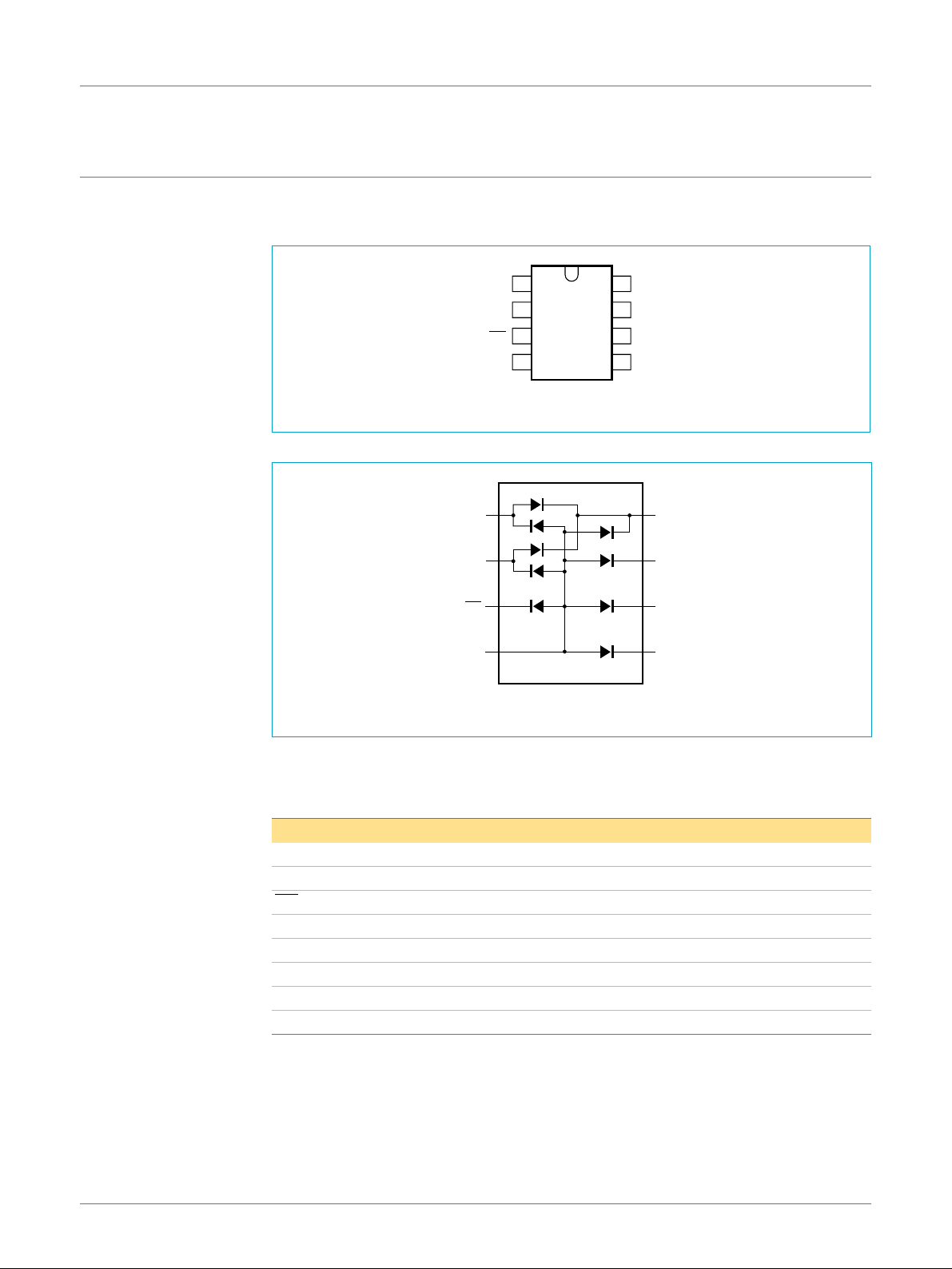
7. Pinning information
7.1 Pinning
PCF8563
Real-time clock/calendar
handbook, halfpage
OSCI
INT
V
SS
1
PCF8563P
2
PCF8563T
3
PCF8563TS
4
Fig 2. Pin configuration.
handbook, halfpage
1
OSCI
V
INT
SS
2
3
4
OSCO
PCF8563
Fig 3. Device diode protection diagram.
MGR885
8
7
6
5
MGR886
V
CLKOUTOSCO
SCL
SDA
8
7
6
5
DD
V
DD
CLKOUT
SCL
SDA
7.2 Pin description
Table 3: Pin description
Symbol Pin Description
OSCI 1 oscillator input
OSCO 2 oscillator output
INT 3 interrupt output (open-drain; active LOW)
V
SS
SDA 5 serial data I/O
SCL 6 serial clock input
CLKOUT 7 clock output (open-drain)
V
DD
9397 750 04855
Product specification 16 April 1999 3 of 30
4 ground
8 positive supply
© Philips Electronics N.V. 1999. All rights reserved.
Page 4

Philips Semiconductors
8. Functional description
The PCF8563 contains sixteen 8-bit registers with an auto-incrementing address
register, an on-chip 32.768 kHz oscillator with an integrated capacitor, a frequency
divider which provides the source clock for the Real-Time Clock (RTC), a
programmable clock output, a timer, an alarm, a voltage-low detector and a 400 kHz
I2C-bus interface.
All 16 registers are designed as addressable 8-bit parallel registers although not all
bits are implemented. The first two registers (memory address 00H and 01H) are
used as control and/or status registers. The memory addresses 02H through 08H are
used as counters for the clock function (seconds up to year counters). Address
locations 09H through 0CH contain alarm registers which define the conditions for an
alarm. Address 0DH controls the CLKOUT output frequency. 0EH and 0FH are the
timer control and timer registers, respectively.
The Seconds, Minutes, Hours, Days, Months, Years as well as the Minute alarm,
Hour alarm and Day alarm registers are all coded in BCD format. The Weekdays and
Weekday alarm register are not coded in BCD format.
PCF8563
Real-time clock/calendar
When one of the RTC registers is read the contents of all counters are frozen.
Therefore, faulty reading of the clock/calendar during a carry condition is prevented.
8.1 Alarm function modes
By clearing the MSB (bit AE = Alarm Enable) of one or more of the alarm registers,
the corresponding alarm condition(s) will be active. In this way an alarm can be
generated from once per minute up to once per week. The alarm condition sets the
alarm flag, AF (bit 3 of Control/Status 2 register). The asserted AF can be used to
generate an interrupt (INT). Bit AF can only be cleared by software.
8.2 Timer
The 8-bit countdown timer (address 0FH) is controlled by the Timer Control register
(address 0EH; see Table 25). The Timer Control register selects one of 4 source
clock frequencies for the timer (4096, 64, 1, or1⁄60Hz), and enables/disables the
timer. The timer counts down from a software-loaded 8-bit binary value. At the end of
every countdown, the timer sets the timer flag TF (see Table 7). The timer flag TF can
only be cleared by software. The asserted timer flag TF can be used to generate an
interrupt (INT). The interrupt may be generated as a pulsed signal every countdown
period or as a permanently active signal which follows the condition of TF. TI/TP (see
Table 7) is used to control this mode selection. When reading the timer, the current
countdown value is returned.
8.3 CLKOUT output
A programmable square wave is availableat the CLKOUT pin. Operation is controlled
by the CLKOUT frequency register (address 0DH; see Table 23). Frequencies of
32.768 kHz (default), 1024, 32 and 1 Hz can be generated for use as a system clock,
microcontroller clock, input to a charge pump, or for calibration of the oscillator.
CLKOUT is an open-drain output and enabled at power-on. If disabled it becomes
high-impedance.
9397 750 04855
Product specification 16 April 1999 4 of 30
© Philips Electronics N.V. 1999. All rights reserved.
Page 5
Philips Semiconductors
8.4 Reset
The PCF8563 includes an internal reset circuit which is active whenever the oscillator
is stopped. In the reset state the I2C-bus logic is initialized and all registers, including
the address pointer, are cleared with the exception of bits FE, VL, TD1, TD0, TESTC
and AE which are set to logic 1.
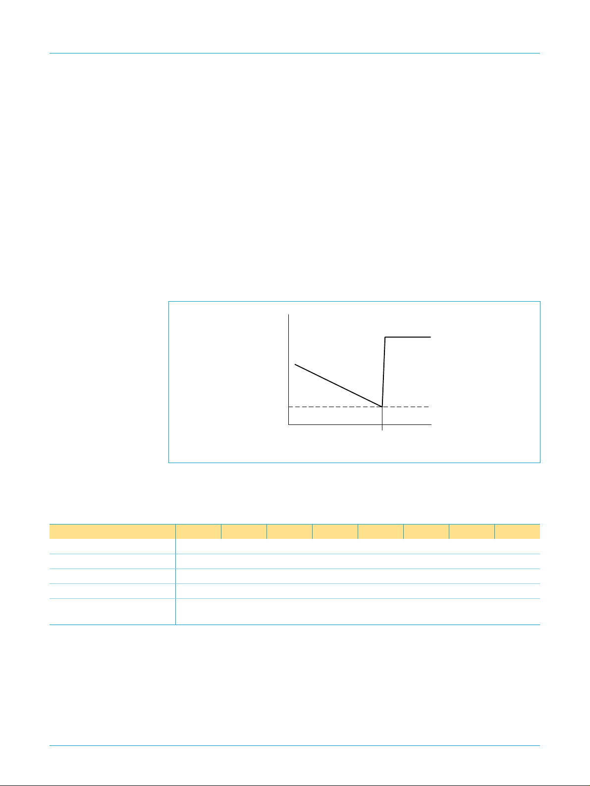
8.5 Voltage-low detector and clock monitor
PCF8563
Real-time clock/calendar
The PCF8563 has an on-chip voltage-low detector. When VDD drops below V
VL bit (Voltage Low, bit 7 in the Seconds register) is set to indicate that reliable
clock/calendar information is no longer guaranteed. The VL flag can only be cleared
by software.
The VL bit is intended to detect the situation when VDD is decreasing slowly for
example under battery operation. Should VDDreach V
before power is re-asserted
low
then the VL bit will be set. This will indicate that the time may be corrupted.
handbook, halfpage
V
DD
V
low
Fig 4. Voltage-low detection.
period of battery
operation
VL set
MGR887
normal power
operation
t
8.6 Register organization
low
the
Table 4: Registers overview
Bit positions labelled as ‘−’are not implemented; those labelled with ‘0’ should always be written with logic 0.
Address Register name Bit 7 Bit 6 Bit 5 Bit 4 Bit 3 Bit 2 Bit 1 Bit 0
00H Control/Status 1 TEST1 0 STOP 0 TESTC 0 0 0
01H Control/Status 2 0 0 0 TI/TP AF TF AIE TIE
0DH CLKOUT frequency FE −−−−−FD1 FD0
0EH Timer control TE −−−−−TD1 TD0
0FH Timer countdown
value
9397 750 04855
Product specification 16 April 1999 5 of 30
<timer countdown value>
© Philips Electronics N.V. 1999. All rights reserved.
Page 6

Philips Semiconductors
PCF8563
Real-time clock/calendar
Table 5: BCD formatted registers overview
Bit positions labelled as ‘−’are not implemented.
Address Register name BCD format tens nibble BCD format units nibble
Bit 7 Bit 6 Bit 5 Bit 4 Bit 3 Bit 2 Bit 1 Bit 0
3
2
02H Seconds VL <seconds 00 to 59 coded in BCD>
03H Minutes − <minutes 00 to 59 coded in BCD>
04H Hours −− <hours 00 to 23 coded in BCD>
05H Days −− <days 01 to 31 coded in BCD>
06H Weekdays −−−−− <weekdays 0 to 6 >
07H Months/Century C −− <months 01 to 12 coded in BCD>
08H Years <years 00 to 99 coded in BCD>
09H Minute alarm AE <minute alarm 00 to 59 coded in BCD>
0AH Hour alarm AE − <hour alarm 00 to 23 coded in BCD>
0BH Day alarm AE − <day alarm 01 to 31 coded in BCD>
0CH Weekday alarm AE −−−− <weekday alarm 0 to 6 >
2
2
1
2
0
2
3
2
2
2
1
2
0
2
[1]
[1]
[1] Not coded in BCD.
8.6.1 Control/Status 1 register
Table 6: Control/Status 1 register bits description (address 00H)
Bit Symbol Description
7 TEST1 TEST1 = 0; normal mode.
TEST1 = 1; EXT_CLK test mode; see Section 8.7.
5 STOP STOP = 0; RTC source clock runs.
STOP = 1; all RTC divider chain flip-flops are asynchronously set
to logic 0; the RTC clock is stopped (CLKOUT at 32.768 kHz is still
available).
3 TESTC TESTC = 0; power-on reset override facility is disabled (set to logic 0
for normal operation).
TESTC = 1; power-on reset override is enabled.
6, 4, 2 to 0 0 By default set to logic 0.
9397 750 04855
Product specification 16 April 1999 6 of 30
© Philips Electronics N.V. 1999. All rights reserved.
Page 7

Philips Semiconductors
8.6.2 Control/Status 2 register
Table 7: Description of Control/Status 2 register bits description (address 01H)
Bit Symbol Description
7 to 5 0 By default set to logic 0.
4 TI/TP TI/TP = 0: INT is active when TF is active (subject to the status of TIE).
3 AF When an alarm occurs, AF is set to logic 1. Similarly, at the end of a
2TF
1 AIE Bits AIE and TIE activate or deactivate the generation of an interrupt
0 TIE
PCF8563
Real-time clock/calendar
TI/TP = 1: INT pulses active according to Table 8 (subjectto the status
of TIE). Note that if AF and AIE are active then INT will be permanently
active.
timer countdown, TF is set to logic 1. These bits maintain their value
until overwritten by software. If both timer and alarm interrupts are
required in the application, the source of the interrupt can be
determined by reading these bits. To prevent one flag being
overwritten while clearing another, a logic AND is performed during a
write access. See Table 9 for the value descriptions of bits AF and TF.
when AF or TF is asserted, respectively.The interrupt is the logical OR
of these two conditions when both AIE and TIE are set.
AIE = 0: alarm interrupt disabled; AIE = 1: alarm interrupt enabled.
TIE = 0: timer interrupt disabled; TIE = 1: timer interrupt enabled.
Table 8:
Source clock (Hz) INT
4096
64
1
1
⁄
60
[1] TF and INT become active simultaneously.
[2] n = loaded countdown timer value. Timer stopped when n = 0.
INT operation (bit TI/TP = 1)
[1]
period (s)
[2]
n
=1 n>1
1
⁄
8192
1
⁄
128
1
⁄
64
1
⁄
64
Table 9: Value descriptions for bits AF and TF
R/W Bit: AF Bit: TF
Value Description Value Description
Read 0 alarm flag inactive 0 timer flag inactive
1 alarm flag active 1 timer flag active
Write 0 alarm flag is cleared 0 timer flag is cleared
1 alarm flag remains unchanged 1 timer flag remains unchanged
1
⁄
4096
1
⁄
64
1
⁄
64
1
⁄
64
9397 750 04855
Product specification 16 April 1999 7 of 30
© Philips Electronics N.V. 1999. All rights reserved.
Page 8

Philips Semiconductors
8.6.3 Seconds, Minutes and Hours registers
Table 10: Seconds/VL register bits description (address 02H)
Bit Symbol Description
7 VL VL = 0: reliable clock/calendar information is guaranteed;
6 to 0 <seconds> These bits represent the current seconds value coded in BCD
Table 11: Minutes register bits description (address 03H)
Bit Symbol Description
7 − not implemented
6 to 0 <minutes> These bits represent the current minutes value coded in BCD
Table 12: Hours register bits description (address 04H)
Bit Symbol Description
7 to 6 − not implemented
5 to 0 <hours> These bits represent the current hours value coded in BCD format;
PCF8563
Real-time clock/calendar
VL = 1: reliable clock/calendar information is no longer
guaranteed.
format; value = 00 to 59.
Example: <seconds> = 101 1001, represents the value 59 s.
format; value = 00 to 59.
value=00to23.
8.6.4 Days, Weekdays, Months/Century and Years registers
Table 13: Days register bits description (address 05H)
Bit Symbol Description
7 to 6 − not implemented
5 to 0 <days> These bits represent the current day value coded in BCD format;
value = 01 to 31.
The PCF8563 compensates for leap years by adding a 29th day to
February if the year counter contains a value which is exactly
divisible by 4, including the year ‘00’.
Table 14: Weekdays register bits description (address 06H)
Bit Symbol Description
7 to 3 − not implemented
2 to 0 <weekdays> These bits represent the current weekday value 0 to 6;
see Table 15.
These bits may be re-assigned by the user.
9397 750 04855
Product specification 16 April 1999 8 of 30
© Philips Electronics N.V. 1999. All rights reserved.
Page 9

Philips Semiconductors
Table 15: Weekday assignments
Day Bit 2 Bit 1 Bit 0
Sunday 0 0 0
Monday 0 0 1
Tuesday 0 1 0
Wednesday 0 1 1
Thursday 1 0 0
Friday 1 0 1
Saturday 1 1 0
Table 16: Months/Century register bits description (address 07H)
Bit Symbol Description
7 C Century bit. C = 0; indicates the century is 20xx.
6to5 − not implemented
4 to 0 <months> These bits represents the current month value coded in BCD format;
PCF8563
Real-time clock/calendar
C = 1; indicates the century is 19xx. ‘xx’ indicates the value held in the
Years register; see Table 18.
This bit is toggled when the Years register overflows from 99 to 00.
These bits may be re-assigned by the user.
value = 01 to 12; see Table 17.
Table 17: Month assignments
Month Bit 4 Bit 3 Bit 2 Bit 1 Bit 0
January00001
February00010
March 00011
April 00100
May 00101
June 00110
July 00111
August 01000
September 01001
October 10000
November 10001
December 10010
Table 18: Years register bits description (address 08H)
Bit Symbol Description
7 to 0 <years> This register represents the current year value coded in BCD
format; value = 00 to 99.
9397 750 04855
Product specification 16 April 1999 9 of 30
© Philips Electronics N.V. 1999. All rights reserved.
Page 10

Philips Semiconductors
8.6.5 Alarm registers
When one or more of the alarm registers are loaded with a valid minute, hour, day or
weekday and its corresponding AE (Alarm Enable) bit is a logic 0, then that
information will be compared with the current minute, hour, day and weekday. When
all enabled comparisons first match, the bit AF (Alarm Flag) is set.
AF will remain set until cleared by software. Once AF has been cleared it will only be
set again when the time increments to match the alarm condition once more. Alarm
registers which have their AE bit set at logic 1 will be ignored.
Table 19: Minute alarm register bits description (address 09H)
Bit Symbol Description
7 AE AE = 0; minute alarm is enabled. AE = 1; minute alarm is disabled.
6 to 0 <minute alarm> These bits represents the minute alarm information coded in BCD
Table 20: Hour alarm register bits description (address 0AH)
Bit Symbol Description
7 AE AE = 0; hour alarm is enabled. AE = 1; hour alarm is disabled.
6 to 0 <hour alarm> These bits represents the hour alarm information coded in BCD
PCF8563
Real-time clock/calendar
format; value = 00 to 59.
format; value = 00 to 23.
Table 21: Day alarm register bits description (address 0BH)
Bit Symbol Description
7 AE AE = 0; day alarm is enabled. AE = 1; day alarm is disabled.
6 to 0 <day alarm> These bits represents the day alarm information coded in BCD
format; value = 01 to 31.
Table 22: Weekday alarm register bits description (address 0CH)
Bit Symbol Description
7 AE AE = 0; weekday alarm is enabled.
AE = 1; weekday alarm is disabled.
6 to 0 <weekday alarm> These bits represents the weekday alarm information
value0to6.
9397 750 04855
Product specification 16 April 1999 10 of 30
© Philips Electronics N.V. 1999. All rights reserved.
Page 11

Philips Semiconductors
8.6.6 CLKOUT frequency register
Table 23: CLKOUT frequency register bits description (address 0DH)
Bit Symbol Description
7 FE FE = 0; the CLKOUT output is inhibited and the CLKOUT output is
6to2 − not implemented
1 FD1 These bits control the frequency output (f
0 FD0
Table 24: CLKOUT frequency selection
Real-time clock/calendar
set to high-impedance. FE = 1; the CLKOUT output is activated.
pin; see Table 24.
FD1 FD0 f
0 0 32.768 kHz
0 1 1 024 Hz
1 0 32 Hz
111Hz
CLKOUT
PCF8563
) on the CLKOUT
CLKOUT
8.6.7 Countdown timer registers
The Timer register is an 8-bit binary countdown timer. It is enabled and disabled via
the Timer control register bit TE. The source clock for the timer is also selected by the
Timer control register. Other timer properties, e.g. interrupt generation, are controlled
via the Control/status 2 register. For accurate read back of the countdown value, the
I2C-bus clock SCL must be operating at a frequency of at least twice the selected
timer clock.
Table 25: Timer control register bits description (address 0EH)
Bit Symbol Description
7 TE TE = 0; timer is disabled. TE = 1; timer is enabled.
6to2 − not implemented
1 TD1 Timer source clock frequency selection bits. These bits determine
0 TD0
Table 26: Timer source clock frequency selection
TD1 TD0 Timer source clock frequency (Hz)
0 0 4096
0164
101
11
the source clock for the countdown timer, see Table 26. When not
in use, TD1 and TD0 should be set to ‘11’ (
saving.
1
⁄
60
1
⁄60Hz) for power
Table 27: Timer countdown value register bits description (address 0FH)
Bit Symbol Description
7 to 0 <timer countdown value> This register holds the loaded countdown value ‘n’.
Countdown period
9397 750 04855
Product specification 16 April 1999 11 of 30
=
--------------------------------------------------------- -
Source clock frequency
© Philips Electronics N.V. 1999. All rights reserved.
n
Page 12

Philips Semiconductors
8.7 EXT_CLK test mode
A test mode is available which allows for on-board testing. In this mode it is possible
to set up test conditions and control the operation of the RTC.
The test mode is entered by setting bit TEST1 in the Control/Status1 register. The
CLKOUT pin then becomes an input. The test mode replaces the internal 64 Hz
signal with the signal that is applied to the CLKOUT pin. Every 64 positive edges
applied to CLKOUT will then generate an increment of one second.
The signal applied to the CLKOUT pin should have a minimum pulse width of 300 ns
and a minimum period of 1000 ns. The internal 64 Hz clock, now sourced from
CLKOUT, is divided down to 1 Hz by a 26 divide chain called a pre-scaler. The
pre-scaler can be set into a known state by using the STOPbit. When the STOP bit is
set, the pre-scaler is reset to 0. STOP must be cleared before the pre-scaler can
operate again. From a STOP condition, the first 1 s increment will take place after
32 positive edges on CLKOUT. Thereafter, every 64 positive edges will cause a 1 s
increment.
Remark: Entry into EXT_CLK test mode is not synchronized to the internal 64 Hz
clock. When entering the test mode, no assumption as to the state of the pre-scaler
can be made.
PCF8563
Real-time clock/calendar
8.7.1 Operation example
1. Enter the EXT_CLK test mode; set bit 7 of Control/Status 1 register (TEST = 1)
2. Set bit 5 of Control/Status 1 register (STOP = 1)
3. Clear bit 5 of Control/Status 1 register (STOP = 0)
4. Set time registers (Seconds, Minutes, Hours, Days, Weekdays, Months/Century
and Years) to desired value
5. Apply 32 clock pulses to CLKOUT
6. Read time registers to see the first change
7. Apply 64 clock pulses to CLKOUT
8. Read time registers to see the second change.
Repeat steps 7 and 8 for additional increments.
8.8 Power-On Reset (POR) override mode
The POR duration is directly related to the crystal oscillator start-up time. Due to the
long start-up times experienced by these types of circuits, a mechanism has been
built in to disable the POR and hence speed up on-board test of the device. The
setting of this mode requires that the I2C-bus pins, SDA and SCL, be toggled in a
specific order as shown in Figure 5. All timing values are required minimum.
Once the override mode has been entered, the chip immediately stops being reset
and normal operation starts i.e. entry into the EXT_CLK test mode via I2C-bus
access. The override mode is cleared by writing a logic 0 to bit TESTC. Re-entry into
the override mode is only possible after TESTC is set to logic 1. Setting TESTC to
logic 0 during normal operation has no effect except to prevent entry into the POR
override mode.
9397 750 04855
Product specification 16 April 1999 12 of 30
© Philips Electronics N.V. 1999. All rights reserved.
Page 13

Philips Semiconductors
PCF8563
Real-time clock/calendar
handbook, full pagewidth
SDA
SCL
8 ms
power up
Fig 5. POR override sequence.
8.9 Serial interface
The serial interface of the PCF8563 is the I2C-bus. A detailed description of the
I2C-bus specification, including applications, is given in the brochure:
and how to use it
8.9.1 Characteristics of the I2C-bus
The I2C-bus is for bidirectional, two-line communication between different ICs or
modules. The two lines are a serial data line (SDA) and a serial clock line (SCL). Both
lines must be connected to a positive supply via a pull-up resistor. Data transfer may
be initiated only when the bus is not busy.
The I2C-bus system configuration is shown in Figure 6. A device generating a
message is a ‘transmitter’, a device receiving a message is the ‘receiver’. The device
that controls the message is the ‘master’ and the devices which are controlled by the
master are the ‘slaves’.
500 ns 2000 ns
, order no. 9398 393 40011 or
override active
MGM664
The I2C-bus
I2C Peripherals Data Handbook IC12.
SDA
SCL
MASTER
TRANSMITTER /
RECEIVER
SLAVE
RECEIVER
Fig 6. I2C-bus system configuration.
8.9.2 START and STOP conditions
Both data and clock lines remain HIGH when the bus is not busy. A HIGH-to-LOW
transition of the data line, while the clock is HIGH is defined as the start condition (S).
A LOW-to-HIGH transition of the data line while the clock is HIGH is defined as the
stop condition (P); see Figure 7.
idth
SDA
SCL
Fig 7. START and STOP conditions on the I2C-bus.
S
START condition
SLAVE
TRANSMITTER /
RECEIVER
MASTER
TRANSMITTER
STOP condition
P
MASTER
TRANSMITTER /
RECEIVER
MBA605
SDA
SCL
MBC622
9397 750 04855
Product specification 16 April 1999 13 of 30
© Philips Electronics N.V. 1999. All rights reserved.
Page 14

Philips Semiconductors
8.9.3 Bit transfer
One data bit is transferred during each clock pulse. The data on the SDA line must
remain stable during the HIGH period of the clock pulse as changes in the data line at
this time will be interpreted as a control signal; see Figure 8.
PCF8563
Real-time clock/calendar
th
SDA
SCL
Fig 8. Bit transfer on the I2C-bus.
8.9.4 Acknowledge
The number of data bytes transferred between the START and STOP conditions from
transmitter to receiver is unlimited. Each byte of eight bits is followed by an
acknowledge bit. The acknowledge bit is a HIGH level signal put on the bus by the
transmitter during which time the master generates an extra acknowledge related
clock pulse.
A slave receiver which is addressed must generate an acknowledge after the
reception of each byte. Also a master receiver must generate an acknowledge after
the reception of each byte that has been clocked out of the slave transmitter.
The device that acknowledges must pull down the SDA line during the acknowledge
clock pulse, so that the SDA line is stable LOW during the HIGH period of the
acknowledge related clock pulse (set-up and hold times must be taken into
consideration).
A master receiver must signal an end of data to the transmitter by not generating an
acknowledge on the last byte that has been clocked out of the slave. In this event the
transmitter must leave the data line HIGH to enable the master to generate a STOP
condition.
data line
stable;
data valid
change
of data
allowed
MBC621
idth
DATA OUTPUT
BY TRANSMITTER
not acknowledge
DATA OUTPUT
BY RECEIVER
acknowledge
SCL FROM
MASTER
S
START
condition
9821
clock pulse for
acknowledgement
MBC602
Fig 9. Acknowledge on the I2C-bus.
9397 750 04855
Product specification 16 April 1999 14 of 30
© Philips Electronics N.V. 1999. All rights reserved.
Page 15

Philips Semiconductors
8.9.5 I2C-bus protocol
Addressing: Before any data is transmitted on the I2C-bus, the device which should
respond is addressed first. The addressing is always carried out with the first byte
transmitted after the start procedure.
The PCF8563 acts as a slave receiver or slave transmitter. Therefore the clock signal
SCL is only an input signal, but the data signal SDA is a bidirectional line.
The PCF8563 slave address is shown in Figure 10.
PCF8563
Real-time clock/calendar
handbook, halfpage
1 0 1 0 0 0 A0 R/W
group 1
group 2
MRB016
Fig 10. Slave address.
Clock/calendar read/write cycles: The I2C-bus configuration for the different
PCF8563 read and write cycles are shown in Figure 11, 12 and 13. The word
address is a four bit value that defines which register is to be accessed next. The
upper four bits of the word address are not used.
idth
acknowledgement
from slave
S 0ASLAVE ADDRESS WORD ADDRESS A ADATA P
R/W
acknowledgement
from slave
Fig 11. Master transmits to slave receiver (write mode).
n bytes
acknowledgement
from slave
auto increment
memory word address
MBD822
9397 750 04855
Product specification 16 April 1999 15 of 30
© Philips Electronics N.V. 1999. All rights reserved.
Page 16

Philips Semiconductors
PCF8563
Real-time clock/calendar
handbook, full pagewidth
S 0ASLAVE ADDRESS WORD ADDRESS A A
acknowledgement
from slave
R/W
acknowledgement
from slave
SLAVE ADDRESS
S1
at this moment master-transmitter
becomes master receiver and
PCF8563 slave-receiver
becomes slave-transmitter
acknowledgement
from slave
R/W
MGL409
Fig 12. Master reads after setting word address (write word address; read data).
handbook, full pagewidth
acknowledgement
from slave
acknowledgement
from master
no acknowledgement
acknowledgement
DATA
n bytes
auto increment
memory word address
last byte
from master
from master
A
no acknowledgement
from master
P
1DATA
auto increment
memory word address
S
SLAVE ADDRESS DATA
1A
R/W
A1DATA
n bytes last byte
auto increment
word address
auto increment
word address
P
MGL665
Fig 13. Master reads slave immediately after first byte (read mode).
9. Limiting values
Table 28: Limiting values
In accordance with the Absolute Maximum Rating System (IEC 60134).
Symbol Parameter Conditions Min Max Unit
V
DD
I
DD
V
I
V
O
I
I
I
O
P
tot
T
amb
T
stg
supply voltage −0.5 +6.5 V
supply current −50 +50 mA
input voltage on inputs SCL and SDA −0.5 6.5 V
input voltage on input OSCI −0.5 V
+ 0.5 V
DD
output voltage on outputs CLKOUT and INT −0.5 6.5 V
DC input current at any input −10 +10 mA
DC output current at any output −10 +10 mA
total power dissipation − 300 mW
operating ambient temperature −40 +85 °C
storage temperature −65 +150 °C
9397 750 04855
© Philips Electronics N.V. 1999. All rights reserved.
Product specification 16 April 1999 16 of 30
Page 17

Philips Semiconductors
PCF8563
Real-time clock/calendar
10. Static characteristics
Table 29: Static characteristics
VDD= 1.8 to 5.5 V; VSS=0V; T
specified.
Symbol Parameter Conditions Min Typ Max Unit
Supplies
V
DD
supply voltage I2C-bus inactive; T
supply voltage for reliable
clock/calendar information
I
DD1
supply current;
CLKOUT disabled (FE = 0)
I
DD2
supply current;
CLKOUTenabled
(f
= 32 kHz; FE = 1)
CLKOUT
Inputs
V
IL
V
IH
I
LI
C
i
LOW-level input voltage V
HIGH-level input voltage 0.7V
input leakage current VI=VDDor V
input capacitance
Outputs
I
OL(SDA)
LOW-level output current;
pin SDA
I
OL(INT)
I
OL(CLKOUT)
LOW-level output current;
INT
pin
LOW-level output current;
pin CLKOUT
=−40 to 85°C; f
amb
= 32.768 kHz; quartz Rs=40kΩ; CL= 8 pF; unless otherwise
OSC
=25°C 1.0
amb
2
C-bus active; f
I
=25°CV
T
amb
f
= 400 kHz
SCL
= 100 kHz −− 200 µA
f
SCL
= 0 Hz; T
f
SCL
= 400 kHz 1.8
SCL
=25°C
amb
[1]
− 5.5 V
[1]
− 5.5 V
low
[2]
−− 800 µA
[2]
− 5.5 V
VDD=5V − 275 550 nA
=3V − 250 500 nA
V
DD
=2V − 225 450 nA
V
DD
f
SCL
=0Hz
[2]
VDD=5V − 500 750 nA
=3V − 400 650 nA
V
DD
=2V − 400 600 nA
V
DD
f
SCL
= 0 Hz; T
amb
=25°C
[2]
VDD=5V − 825 1600 nA
=3V − 550 1000 nA
V
DD
=2V − 425 800 nA
V
DD
f
SCL
=0Hz
[2]
VDD=5V − 950 1700 nA
=3V − 650 1100 nA
V
DD
=2V − 500 900 nA
V
DD
SS
SS
− 0.3V
− V
DD
DD
DD
−1 − +1 µA
[3]
−− 7pF
V
V
VOL= 0.4 V; VDD=5V −3 −−mA
−1 −−mA
−1 −−mA
9397 750 04855
Product specification 16 April 1999 17 of 30
© Philips Electronics N.V. 1999. All rights reserved.
Page 18

Philips Semiconductors
PCF8563
Real-time clock/calendar
Table 29: Static characteristics
VDD= 1.8 to 5.5 V; VSS=0V; T
…continued
=−40 to 85°C; f
amb
= 32.768 kHz; quartz Rs=40kΩ; CL= 8 pF; unless otherwise
OSC
specified.
Symbol Parameter Conditions Min Typ Max Unit
I
OH(CLKOUT)
HIGH-level output current;
VOH= 4.6 V; VDD=5V 1 −−mA
pin CLKOUT
I
LO
output leakage current VO=VDDor V
SS
−1 − +1 µA
Voltage detector
V
low
voltage-low detection level T
[1] For reliable oscillator start-up at power-up: V
[2] Timer source clock =1⁄60Hz; SCL and SDA = V
[3] Tested on sample basis.
I
DD
(µA)
1
0.8
0.6
handbook, halfpage
=25°C − 0.9 1.0 V
amb
DD(min)power-up
DD.
MGR888
= V
DD(min)
handbook, halfpage
+ 0.3 V.
I
DD
(µA)
0.8
0.6
1
MGR889
0.4
0.2
0
02 6
T
=25°C; Timer = 1 minute. T
amb
4
VDD (V)
0.4
0.2
0
02 6
=25°C; Timer = 1 minute.
amb
4
VDD (V)
Fig 14. IDD as a function of VDD; CLKOUT disabled. Fig 15. IDD as a function of VDD; CLKOUT = 32 kHz.
handbook, halfpage
1
I
DD
(µA)
0.8
0.6
0.4
0.2
0
−40 0 40 120
MGR890
handbook, halfpage
4
frequency
deviation
(ppm)
2
0
−2
−4
80
T (°C)
02 6
4
MGR891
VDD (V)
VDD= 3 V; Timer = 1 minute. T
Fig 16. IDD as a function of T
9397 750 04855
; CLKOUT = 32 kHz. Fig 17. Frequency deviation as function of VDD.
amb
=25°C; normalized to VDD=3V.
amb
© Philips Electronics N.V. 1999. All rights reserved.
Product specification 16 April 1999 18 of 30
Page 19

Philips Semiconductors
PCF8563
Real-time clock/calendar
11. Dynamic characteristics
Table 30: Dynamic characteristics
VDD= 1.8 to 5.5 V; VSS=0V; T
specified.
Symbol Parameter Conditions Min Typ Max Unit
Oscillator
C
L(integrated)
∆f
OSC/fOSC
integrated load capacitance 15 25 35 pF
oscillator stability ∆VDD= 200 mV; T
Quartz crystal parameters (f
R
s
C
L
C
T
series resistance −−40 kΩ
parallel load capacitance − 10 − pF
trimmer capacitance 5 − 25 pF
CLKOUT output
δ
CLKOUT
2
C-bus timing characteristics
I
f
SCL
t
HD;STA
t
SU;STA
CLKOUT duty factor
SCL clock frequency
START condition hold time 0.6 −−µs
set-up time for a repeated
START condition
t
LOW
t
HIGH
t
r
t
f
C
b
t
SU;DAT
t
HD;DAT
t
SU;STO
t
SW
SCL LOW time 1.3 −−µs
SCL HIGH time 0.6 −−µs
SCL and SDA rise time −−0.3 µs
SCL and SDA fall time −−0.3 µs
capacitive bus line load −−400 pF
data set-up time 100 −−ns
data hold time 0 −−ns
set-up time for STOP condition 4.0 −−µs
tolerable spike width on bus −−50 ns
=−40 to +85°C; f
amb
= 32.768 kHz)
OSC
[2]
= 32.768 kHz; quartz Rs=40kΩ; CL= 8 pF; unless otherwise
OSC
=25°C − 2×10⁻⁷−
amb
[1]
− 50 − %
[3]
−−400 kHz
0.6 −−µs
[1] Unspecified for f
[2] All timing values are valid within the operating supply voltage range at T
VSSto VDD.
[3] I2C-bus access time between two STARTs or between a START and a STOP condition to this device must be less than one second.
9397 750 04855
Product specification 16 April 1999 19 of 30
CLKOUT
= 32.768 kHz.
and referenced to VILand VIHwith an input voltage swing of
amb
© Philips Electronics N.V. 1999. All rights reserved.
Page 20

Philips Semiconductors
ok, full pagewidth
SDA
PCF8563
Real-time clock/calendar
t
BUF
SCL
SDA
MGA728
Fig 18. I2C-bus timing waveforms.
t
HD;STA
t
LOW
t
r
t
SU;STA
t
HD;DAT
t
HIGH
t
f
t
SU;DAT
t
SU;STO
9397 750 04855
© Philips Electronics N.V. 1999. All rights reserved.
Product specification 16 April 1999 20 of 30
Page 21

Philips Semiconductors
12. Application information
PCF8563
Real-time clock/calendar
handbook, full pagewidth
Fig 19. Application diagram.
1 F
V
CLOCK CALENDAR
OSCI
PCF8563
OSCO
V
DD
SS
SCL
SDA
SDA SCL
2
C-bus)
(I
SDA
SCL
MASTER
TRANSMITTER/
RECEIVER
V
DD
RR
V
DD
R: pull-up resistor
t
r
R =
C
b
MGM665
12.1 Quartz crystal frequency adjustment
Method 1: Fixed OSCI capacitor — By evaluating the average capacitance
necessary for the application layout a fixed capacitor can be used. The frequency is
best measured via the 32.768 kHz signal available after power-on at the CLKOUT
pin. The frequency tolerance depends on the quartz crystal tolerance, the capacitor
tolerance and the device-to-device tolerance (on average ±5 × 10⁻⁶).
Average deviations of ±5 minutes per year can be easily achieved.
Method 2: OSCI trimmer — The oscillator is tuned to the required accuracy by
adjusting a trimmer capacitor on pin OSCI and measuring the 32.768 kHz signal
available after power-on at the CLKOUT pin.
Method 3: OSCO output — Direct output measurement on pin OSCO (accounting
for test probe capacitance).
9397 750 04855
Product specification 16 April 1999 21 of 30
© Philips Electronics N.V. 1999. All rights reserved.
Page 22

Philips Semiconductors
13. Package outline
PCF8563
Real-time clock/calendar
SO8: plastic small outline package; 8 leads; body width 3.9 mm
D
c
y
Z
8
pin 1 index
1
e
5
A
2
A
4
w M
b
p
SOT96-1
E
H
E
1
detail X
A
X
v M
A
Q
A
(A )
3
L
p
L
θ
0 2.5 5 mm
scale
DIMENSIONS (inch dimensions are derived from the original mm dimensions)
A
UNIT
mm
inches
Notes
1. Plastic or metal protrusions of 0.15 mm maximum per side are not included.
2. Plastic or metal protrusions of 0.25 mm maximum per side are not included.
OUTLINE
VERSION
SOT96-1
max.
1.75
0.069
A
1A2A3
0.25
1.45
0.10
1.25
0.010
0.057
0.004
0.049
IEC JEDEC EIAJ
076E03S MS-012AA
0.25
0.01
b
0.49
0.36
0.019
0.014
p
0.0100
0.0075
cD
0.25
5.0
0.19
4.8
0.20
0.19
REFERENCES
(1)E(2)
4.0
3.8
0.16
0.15
eHELLpQZywv θ
1.27
0.050
6.2
5.8
0.244
0.228
1.05
1.0
0.4
0.039
0.016
0.7
0.6
0.028
0.024
0.25 0.10.25
0.010.010.041 0.004
EUROPEAN
PROJECTION
(1)
0.7
0.3
0.028
0.012
ISSUE DATE
95-02-04
97-05-22
o
8
o
0
Fig 20. SOT96-1.
9397 750 04855
Product specification 16 April 1999 22 of 30
© Philips Electronics N.V. 1999. All rights reserved.
Page 23

Philips Semiconductors
PCF8563
Real-time clock/calendar
DIP8: plastic dual in-line package; 8 leads (300 mil)
D
seating plane
A
L
Z
e
b
8
pin 1 index
1
w M
b
1
b
2
5
SOT97-1
M
E
A
2
A
c
(e )
1
M
H
E
1
DIMENSIONS (inch dimensions are derived from the original mm dimensions)
A
A
A
UNIT
max.
mm
inches
Note
1. Plastic or metal protrusions of 0.25 mm maximum per side are not included.
OUTLINE
VERSION
SOT97-1
12
min.
max.
050G01 MO-001AN
b
1.73
1.14
0.068
0.045
IEC JEDEC EIAJ
b
1
0.53
0.38
0.021
0.015
4
0 5 10 mm
b
2
1.07
0.89
0.042
0.035
REFERENCES
Fig 21. SOT97-1.
scale
(1) (1)
cD E e M
0.36
9.8
9.2
0.39
0.36
6.48
6.20
0.26
0.24
0.23
0.014
0.009
L
3.60
8.25
3.05
7.80
0.14
0.32
0.12
0.31
EUROPEAN
PROJECTION
M
E
10.0
8.3
0.39
0.33
e
1
H
0.2542.54 7.62
ISSUE DATE
w
0.010.10 0.30
92-11-17
95-02-04
(1)
Z
max.
1.154.2 0.51 3.2
0.0450.17 0.020 0.13
9397 750 04855
© Philips Electronics N.V. 1999. All rights reserved.
Product specification 16 April 1999 23 of 30
Page 24

Philips Semiconductors
PCF8563
Real-time clock/calendar
TSSOP8: plastic thin shrink small outline package; 8 leads; body width 3 mm
D
y
Z
8
pin 1 index
5
14
w
e
b
p
M
c
A
2
A
1
E
H
E
detail X
A
(A3)
L
p
L
X
v
M
A
A
θ
SOT505-1
2.5 5 mm0
scale
DIMENSIONS (mm are the original dimensions)
A
A
0.15
0.05
1
A2A3b
0.95
0.80
IEC JEDEC EIAJ
0.25
0.45
0.25
p
UNIT
max.
mm
1.10
Notes
1. Plastic or metal protrusions of 0.15 mm maximum per side are not included.
2. Plastic or metal protrusions of 0.25 mm maximum per side are not included.
OUTLINE
VERSION
SOT505-1
(1)E(2)
ceD
0.28
3.10
3.10
0.15
REFERENCES
2.90
2.90
0.65
5.10
4.70
LH
E
L
0.70
0.40
p
wyv
0.1 0.10.10.94
EUROPEAN
PROJECTION
(1)
Z
0.70
0.35
ISSUE DATE
θ
6°
0°
99-04-09
Fig 22. SOT505-1.
9397 750 04855
Product specification 16 April 1999 24 of 30
© Philips Electronics N.V. 1999. All rights reserved.
Page 25

Philips Semiconductors
14. Soldering
14.1 Introduction
This text gives a very brief insight to a complex technology. A more in-depth account
of soldering ICs can be found in our
Packages
There is no soldering method that is ideal for all IC packages. Wave soldering is often
preferred when through-hole and surface mount components are mixed on one
printed-circuit board. However, wave soldering is not always suitable for surface
mount ICs, or for printed-circuit boards with high population densities. In these
situations reflow soldering is often used.
14.2 Surface mount packages
14.2.1 Reflow soldering
Reflow soldering requires solder paste (a suspension of fine solder particles, flux and
binding agent) to be applied to the printed-circuit board by screen printing, stencilling
or pressure-syringe dispensing before package placement.
PCF8563
Real-time clock/calendar
Data Handbook IC26; Integrated Circuit
(document order number 9398 652 90011).
Several methods exist for reflowing; for example, infrared/convection heating in a
conveyor type oven. Throughput times (preheating, soldering and cooling) vary
between 100 and 200 seconds depending on heating method.
Typical reflow peak temperatures range from 215 to 250 °C. The top-surface
temperature of the packages should preferable be kept below 230 °C.
14.2.2 Wave soldering
Conventional single wave soldering is not recommended for surface mount devices
(SMDs) or printed-circuit boards with a high component density, as solder bridging
and non-wetting can present major problems.
To overcome these problems the double-wave soldering method was specifically
developed.
If wave soldering is used the following conditions must be observed for optimal
results:
Use a double-wave soldering method comprising a turbulent wave with high
•
upward pressure followed by a smooth laminar wave.
For packages with leads on two sides and a pitch (e):
•
– larger than or equal to 1.27 mm, the footprint longitudinal axis is preferred to be
parallel to the transport direction of the printed-circuit board;
– smaller than 1.27 mm, the footprint longitudinal axis must be parallel to the
transport direction of the printed-circuit board.
The footprint must incorporate solder thieves at the downstream end.
For packages with leads on four sides, the footprint must be placed at a 45° angle
•
to the transport direction of the printed-circuit board. The footprint must
incorporate solder thieves downstream and at the side corners.
9397 750 04855
Product specification 16 April 1999 25 of 30
© Philips Electronics N.V. 1999. All rights reserved.
Page 26

Philips Semiconductors
During placement and before soldering, the package must be fixed with a droplet of
adhesive. The adhesive can be applied by screen printing, pin transfer or syringe
dispensing. The package can be soldered after the adhesive is cured.
Typical dwell time is 4 seconds at 250 °C. A mildly-activated flux will eliminate the
need for removal of corrosive residues in most applications.
14.2.3 Manual soldering
Fix the component by first soldering two diagonally-opposite end leads. Use a low
voltage (24 V or less) soldering iron applied to the flat part of the lead. Contact time
must be limited to 10 seconds at up to 300 °C.
When using a dedicated tool, all other leads can be soldered in one operation within
2 to 5 seconds between 270 and 320 °C.
14.3 Through-hole mount packages
14.3.1 Soldering by dipping or by solder wave
The maximum permissible temperature of the solder is 260 °C; solder at this
temperature must not be in contact with the joints for more than 5 seconds. The total
contact time of successive solder waves must not exceed 5 seconds.
PCF8563
Real-time clock/calendar
The device may be mounted up to the seating plane, but the temperature of the
plastic body must not exceed the specified maximum storage temperature (T
If the printed-circuit board has been pre-heated, forced cooling may be necessary
immediately after soldering to keep the temperature within the permissible limit.
14.3.2 Manual soldering
Apply the soldering iron (24 V or less) to the lead(s) of the package, either below the
seating plane or not more than 2 mm above it. If the temperature of the soldering iron
bit is less than 300 °C it may remain in contact for up to 10 seconds. If the bit
temperature is between 300 and 400 °C, contact may be up to 5 seconds.
stg(max)
).
9397 750 04855
Product specification 16 April 1999 26 of 30
© Philips Electronics N.V. 1999. All rights reserved.
Page 27

Philips Semiconductors
14.4 Package related soldering information
Table 31: Suitability of IC packages for wave, reflow and dipping soldering methods
Mounting Package Soldering method
Through-hole
mount
Surface mount BGA, SQFP not suitable suitable −
[1] All surface mount (SMD) packages are moisture sensitive.Depending upon the moisture content, the
[2] For SDIP packages, the longitudinal axis must be parallel to the transport direction of the
[3] These packages are not suitable for wavesoldering as a solder joint between the printed-circuit board
[4] If wave soldering is considered, then the package must be placed at a 45° angle to the solder wave
[5] Wave soldering is only suitable for LQFP, QFP and TQFP packages with a pitch (e) equal to or larger
[6] Wave soldering is only suitable forSSOP and TSSOP packages with a pitch (e) equal to or larger than
PCF8563
Real-time clock/calendar
Wave Reflow
DBS, DIP, HDIP, SDIP, SIL suitable
HLQFP, HSQFP, HSOP,
not suitable
[2]
[3]
− suitable
suitable −
HTSSOP, SMS
[4]
PLCC
LQFP, QFP, TQFP not recommended
SSOP, TSSOP, VSO not recommended
maximum temperature (with respect to time) and body size of the package, there is a risk that internal
or external package cracks may occur due to vaporization of the moisture in them (the so called
popcorn effect). For details, refer to the Drypack information in the
Circuit Packages; Section: Packing Methods
printed-circuit board.
and heatsink (at bottom version) can not be achieved, and as solder may stick to the heatsink (on top
version).
direction. The package footprint must incorporate solder thieves downstream and at the side corners.
than 0.8 mm; it is definitely not suitable for packages with a pitch (e) equal to or smaller than 0.65 mm.
0.65 mm; it is definitely not suitable for packages with a pitch (e) equal to or smaller than 0.5 mm.
, SO, SOJ suitable suitable −
[4] [5]
suitable −
[6]
suitable −
Data Handbook IC26; Integrated
.
[1]
Dipping
15. Revision history
Rev Date CPCN Description
01 990416 - This data sheet supersedes the version of 1998 Mar 25 (9397 750 03282):
The format of this specification has been redesigned to comply with Philips Semiconductors’
•
new presentation and information standard
Added Figure 3 “Device diode protection diagram.” on page 3
•
Added Figure 4 “Voltage-low detection.” on page 5
•
Added paragraph in Section 8.5 “Voltage-low detector and clock monitor” on page 5
•
Added Figure 14 to 17 on page 18 in Section 10.
•
9397 750 04855
Product specification 16 April 1999 27 of 30
© Philips Electronics N.V. 1999. All rights reserved.
Page 28

Philips Semiconductors
16. Data sheet status
PCF8563
Real-time clock/calendar
Datasheet status Product status Definition
Objective specification Development This data sheet contains the design target or goal specifications for product development. Specification may
change in any manner without notice.
Preliminary specification Qualification This data sheet contains preliminary data, and supplementary data will be published at a later date. Philips
Semiconductors reserves the right to make changes at any time without notice in order to improve design and
supply the best possible product.
Product specification Production This data sheet contains final specifications. Philips Semiconductors reserves the right to make changes at any
time without notice in order to improve design and supply the best possible product.
[1] Please consult the most recently issued data sheet before initiating or completing a design.
17. Definitions
Short-form specification — The data in a short-form specification is
extracted from a full data sheet with the same type number and title. For
detailed information see the relevant data sheet or data handbook.
Limiting values definition — Limiting values given are in accordance with
the Absolute Maximum Rating System (IEC 60134). Stress above one or
more of the limiting values may cause permanent damage to the device.
These are stress ratings only and operation of the device at these or at any
other conditions above those given in the Characteristics sections of the
specification is not implied. Exposure to limiting values for extended periods
may affect device reliability.
Application information — Applications that are described herein for any
of these products are for illustrative purposes only. Philips Semiconductors
make no representation or warranty that such applications will be suitable for
the specified use without further testing or modification.
18. Disclaimers
Life support — These products are not designed for use in life support
appliances, devices, or systems where malfunction of these products can
reasonably be expected to result in personal injury. Philips Semiconductors
[1]
customers using or selling these products for use in such applications do so
at their own risk and agree to fully indemnify Philips Semiconductors for any
damages resulting from such application.
Right to make changes — Philips Semiconductors reserves the right to
make changes, without notice, in the products, including circuits, standard
cells, and/or software, described or contained herein in order to improve
design and/or performance. Philips Semiconductors assumes no
responsibility or liability for the use of any of these products, conveys no
licence or title under any patent, copyright, or mask work right to these
products, and makes no representations or warranties that these products
are free from patent, copyright, or mask work right infringement, unless
otherwise specified.
19. Licenses
Purchase of Philips I2C components
Purchase of Philips I
under the Philips’ I
2
C system provided the system conforms to the I2C specifi-
I
cation defined by Philips. This specification can be ordered
using the code 9398 393 40011.
2
C components conveys a license
2
C patent to use the components in the
9397 750 04855
© Philips Electronics N.V. 1999 All rights reserved.
Product specification 16 April 1999 28 of 30
Page 29

Philips Semiconductors
Real-time clock/calendar
Philips Semiconductors - a worldwide company
PCF8563
Argentina: see South America
Australia: Tel. +61 29 805 4455, Fax. +61 29 805 4466
Austria: Tel. +43 160 101, Fax. +43 160 101 1210
Belarus: Tel. +375 17 220 0733, Fax. +375 17 220 0773
Belgium: see The Netherlands
Brazil: see South America
Bulgaria: Tel. +359 268 9211, Fax. +359 268 9102
Canada: Tel. +1 800 234 7381
China/Hong Kong: Tel. +852 2 319 7888, Fax. +852 2 319 7700
Colombia: see South America
Czech Republic: see Austria
Denmark: Tel. +45 3 288 2636, Fax. +45 3 157 0044
Finland: Tel. +358 961 5800, Fax. +358 96 158 0920
France: Tel. +33 14 099 6161, Fax. +33 14 099 6427
Germany: Tel. +49 40 23 5360, Fax. +49 402 353 6300
Hungary: see Austria
India: Tel. +91 22 493 8541, Fax. +91 22 493 8722
Indonesia: see Singapore
Ireland: Tel. +353 17 64 0000, Fax. +353 17 64 0200
Israel: Tel. +972 36 45 0444, Fax. +972 36 49 1007
Italy: Tel. +39 26 752 2531, Fax. +39 26 752 2557
Japan: Tel. +81 33 740 5130, Fax. +81 33 740 5077
Korea: Tel. +82 27 09 1412, Fax. +82 27 09 1415
Malaysia: Tel. +60 37 50 5214, Fax. +60 37 57 4880
Mexico: Tel. +9-5 800 234 7381
Middle East: see Italy
Netherlands: Tel. +31 40 278 2785, Fax. +31 40 278 8399
New Zealand: Tel. +64 98 49 4160, Fax. +64 98 49 7811
Norway: Tel. +47 22 74 8000, Fax. +47 22 74 8341
Philippines: Tel. +63 28 16 6380, Fax. +63 28 17 3474
Poland: Tel. +48 22 612 2831, Fax. +48 22 612 2327
Portugal: see Spain
Romania: see Italy
Russia: Tel. +7 095 755 6918, Fax. +7 095 755 6919
Singapore: Tel. +65 350 2538, Fax. +65 251 6500
Slovakia: see Austria
Slovenia: see Italy
South Africa: Tel. +27 11 470 5911, Fax. +27 11 470 5494
South America: Tel. +55 11 821 2333, Fax. +55 11 829 1849
Spain: Tel. +34 33 01 6312, Fax. +34 33 01 4107
Sweden: Tel. +46 86 32 2000, Fax. +46 86 32 2745
Switzerland: Tel. +41 14 88 2686, Fax. +41 14 81 7730
Taiwan: Tel. +886 22 134 2865, Fax. +886 22 134 2874
Thailand: Tel. +66 27 45 4090, Fax. +66 23 98 0793
Turkey: Tel. +90 212 279 2770, Fax. +90 212 282 6707
Ukraine: Tel. +380 44 264 2776, Fax. +380 44 268 0461
United Kingdom: Tel. +44 181 730 5000, Fax. +44 181 754 8421
United States: Tel. +1 800 234 7381
Uruguay: see South America
Vietnam: see Singapore
Yugoslavia: Tel. +381 11 62 5344, Fax. +381 11 63 5777
For all other countries apply to: Philips Semiconductors,
Marketing & Sales Communications,
Building BE, P.O. Box 218, 5600 MD EINDHOVEN,
The Netherlands, Fax. +31 40 272 4825
Internet:http://www.semiconductors.philips.com
9397 750 04855
Product specification 16 April 1999 29 of 30
© Philips Electronics N.V. 1999. All rights reserved.
Page 30

Philips Semiconductors
Contents
PCF8563
Real-time clock/calendar
1 General description. . . . . . . . . . . . . . . . . . 1
2 Features . . . . . . . . . . . . . . . . . . . . . . . . . . . 1
3 Applications. . . . . . . . . . . . . . . . . . . . . . . . 1
4 Quick reference data. . . . . . . . . . . . . . . . . 2
5 Ordering information . . . . . . . . . . . . . . . . 2
6 Block diagram . . . . . . . . . . . . . . . . . . . . . . 2
7 Pinning information . . . . . . . . . . . . . . . . . 3
7.1 Pinning . . . . . . . . . . . . . . . . . . . . . . . . . . . 3
7.2 Pin description . . . . . . . . . . . . . . . . . . . . . 3
8 Functional description . . . . . . . . . . . . . . . 4
8.1 Alarm function modes. . . . . . . . . . . . . . . . 4
8.2 Timer . . . . . . . . . . . . . . . . . . . . . . . . . . . . 4
8.3 CLKOUT output . . . . . . . . . . . . . . . . . . . . 4
8.4 Reset . . . . . . . . . . . . . . . . . . . . . . . . . . . . 5
8.5 Voltage-low detector and clock monitor . . 5
8.6 Register organization . . . . . . . . . . . . . . . . 5
8.6.1 Control/Status 1 register . . . . . . . . . . . . . . 6
8.6.2 Control/Status 2 register . . . . . . . . . . . . . . 7
8.6.3 Seconds, Minutes and Hours registers . . . . 8
8.6.4 Days, Weekdays, Months/Century and Years
registers . . . . . . . . . . . . . . . . . . . . . . . . . 8
8.6.5 Alarm registers. . . . . . . . . . . . . . . . . . . . 10
8.6.6 CLKOUT frequency register. . . . . . . . . . . 11
8.6.7 Countdown timer registers. . . . . . . . . . . . 11
8.7 EXT_CLK test mode. . . . . . . . . . . . . . . . 12
8.7.1 Operation example . . . . . . . . . . . . . . . . . 12
8.8 Power-On Reset (POR) override mode . 12
8.9 Serial interface . . . . . . . . . . . . . . . . . . . . 13
8.9.1 Characteristics of the I2C-bus . . . . . . . . . 13
8.9.2 START and STOP conditions . . . . . . . . . 13
8.9.3 Bit transfer. . . . . . . . . . . . . . . . . . . . . . . 14
8.9.4 Acknowledge . . . . . . . . . . . . . . . . . . . . . 14
8.9.5 I2C-bus protocol . . . . . . . . . . . . . . . . . . . 15
9 Limiting values . . . . . . . . . . . . . . . . . . . . 16
10 Static characteristics . . . . . . . . . . . . . . . 17
11 Dynamic characteristics. . . . . . . . . . . . . 19
12 Application information . . . . . . . . . . . . . 21
12.1 Quartz crystal frequency adjustment . . . 21
13 Package outline. . . . . . . . . . . . . . . . . . . . 22
14 Soldering . . . . . . . . . . . . . . . . . . . . . . . . . 25
14.1 Introduction . . . . . . . . . . . . . . . . . . . . . . 25
14.2 Surface mount packages . . . . . . . . . . . . 25
14.2.1 Reflow soldering. . . . . . . . . . . . . . . . . . . 25
14.2.2 Wave soldering . . . . . . . . . . . . . . . . . . . 25
14.2.3 Manual soldering . . . . . . . . . . . . . . . . . . 26
14.3 Through-hole mount packages. . . . . . . . 26
14.3.1 Soldering by dipping or by solder wave. . . 26
14.3.2 Manual soldering . . . . . . . . . . . . . . . . . . 26
14.4 Package related soldering information. . 27
15 Revision history . . . . . . . . . . . . . . . . . . . 27
16 Data sheet status. . . . . . . . . . . . . . . . . . . 28
17 Definitions . . . . . . . . . . . . . . . . . . . . . . . . 28
18 Disclaimers. . . . . . . . . . . . . . . . . . . . . . . . 28
19 Licenses . . . . . . . . . . . . . . . . . . . . . . . . . . 28
© Philips Electronics N.V. 1999. Printed in The Netherlands
All rights are reserved. Reproduction in whole or in part is prohibited without the prior
written consent of the copyright owner.
The information presented in this document does not form part of any quotation or
contract, is believed to be accurate and reliable and may be changed without notice. No
liability will be accepted by the publisher for any consequence of its use. Publication
thereof does not convey nor imply any license under patent- or other industrial or
intellectual property rights.
Date of release: 16 April 1999 Document order number: 9397 750 04855
 Loading...