

Page 1
DATA SH EET
Objective specification
Supersedes data of 1997 Feb 27
File under Integrated Circuits, IC12
1998 Apr 07
INTEGRATED CIRCUITS
PCF8558
Universal LCD driver for small
graphic panels
Page 2
1998 Apr 07 2
Philips Semiconductors Objective specification
Universal LCD driver for small graphic
panels
PCF8558
FEATURES
• Single-chip LCD controller/driver
• 40 row and 101 column outputs
• Display data RAM
40 × 101 bits = 505 bytes = 4040 bits
• On-chip:
– Generation of intermediate LCD bias voltages
– Oscillator requires no external components
(external clock also possible)
• 400 kHz fast I2C-bus interface
• CMOS compatible
• MUX rate 1 : 40
• Logic supply voltage range V
DD
− VSS= 2.5 to 6 V
• Display supply voltage range VDD− V
LCD
= 3.5 to 9 V
• Low power consumption, suitable for battery operated
systems.
APPLICATIONS
• Telecom equipment
• Portable instruments
• Point of sale terminals
• Alarm systems.
GENERAL DESCRIPTION
The PCF8558 is a low power CMOS LCD controller driver,
designed to drive a graphic display of 40 rows and
101 columns. All necessary functions for the display are
provided in a single chip, including on-chip generation of
LCD bias voltages, resulting in a minimum of external
components and lower power consumption.
The PCF8558 interfaces to most microcontrollers via a
I
2
C-bus interface.
ORDERING INFORMATION
Note
1. For further details see Chapter “Bonding pad locations”.
TYPE
NUMBER
PACKAGE
(1)
NAME DESCRIPTION VERSION
PCF8558U/10 − chip on FFC −
PCF8558U/12 − chip with bumps on FFC −
Page 3
1998 Apr 07 3
Philips Semiconductors Objective specification
Universal LCD driver for small graphic
panels
PCF8558
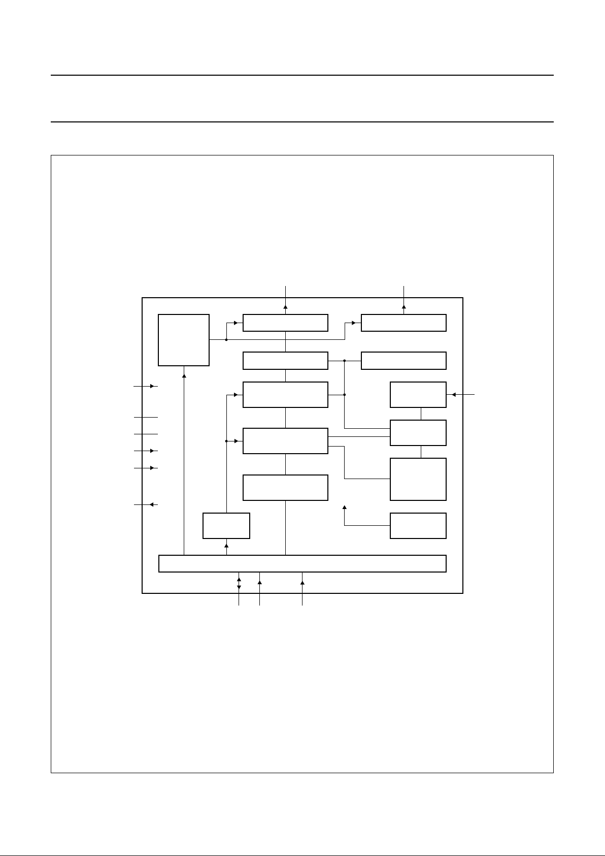
BLOCK DIAGRAM
Fig.1 Block diagram.
handbook, full pagewidth
MGG558
COLUMN DRIVERS
DATA LATCHES
CURSOR AND
DATA CONTROL
DISPLAY DATA RAM
505 BYTES
ADDRESS
COUNTER
DATA
REGISTER
ROW DRIVERS
SHIFT REGISTER
OSCILLATOR
TIMING
GENERATOR
DISPLAY
ADDRESS
COUNTER
POWER-ON
RESET
I/O BUFFER
BIAS
VOLT AGE
GENERATOR
V
LCD
V
DD
V
SS
T1
T3
T2
SDA SCL SA0
OSC
C1 to C101 R1 to R40
PCF8558
Page 4
1998 Apr 07 4
Philips Semiconductors Objective specification
Universal LCD driver for small graphic
panels
PCF8558
PINNING
SYMBOL PAD DESCRIPTION
SCL 1 I
2
C-bus serial clock input
R20 to R1 2 to 21 LCD row driver data outputs
C101 to C1 22 to 122 LCD column driver data outputs
R21 to R40 123 to 142 LCD row driver data outputs
T2 143 test pad output, must be left unconnected (not user accessible)
SDA 144 I
2
C-bus serial data input/output
V
SS
145 ground
T1 146 test pad input, must be connected to V
SS
(not user accessible)
V
LCD
147 negative supply voltage input
SA0 148 the LSB bit of the I
2
C-bus slave address input is set by connecting this pin to either
0(VSS) or 1 (VDD)
T3 149 test pad input, must be connected to V
DD
(not user accessible)
OSC 150 when the on-chip oscillator is used this pin must be connected to V
DD
; an external clock
signal, if used, is input at this pin
V
DD
151 positive supply voltage
Page 5

1998 Apr 07 5
Philips Semiconductors Objective specification
Universal LCD driver for small graphic
panels
PCF8558
FUNCTIONAL DESCRIPTION
LCD bias voltage generator
The intermediate bias voltages for the LCD display are
generated and buffered on-chip. This removes the need
for an external resistor bias chain and significantly reduces
the system power consumption.
Oscillator
The on-chip oscillator provides the clock signal for the
display system. No external components are required and
the OSC pin must be connected to V
DD
.
External clock
If an external clock is to be used it is input at the OSC pin.
The resulting display frame frequency is given by
.
Only in the power-down state is the clock allowed to be
stopped (OSC connected to V
SS
), otherwise the LCD will
be frozen in a state where a DC voltage is applied to it.
Power-on reset
The on-chip power-on reset block initializes the chip after
power-on or power failure. This is a synchronous reset and
requires 2 oscillator cycles to execute. These oscillator
cycles must be provided from the external clock source if
the internal oscillator is not used. If this is not done, the
device may not respond to command sequences
transmitted via the I
2
C-bus interface.
Power-down
The chip can be put into power-down mode where all static
currents are switched off (no internal oscillator, no internal
power-on reset, no bias level generation and all LCD
outputs are internally connected to V
DD
) when
PD = logic 1.
During power-down the information in the RAMs and the
internal chip states are preserved. Instruction execution
during power-down is possible if an externally clock signal
is applied to pad OSC.
Registers
The PCF8558 has one 8-bit register, time shared as a
Command Register (CR) and a Data Register (DR).
The command register stores the command code such as
display on or display off and address information for the
f
frame
f
OSC
3072
------------ -
=
Display Data RAM (DDRAM). Both registers can be written
to but not read from by the system controller.
Address Counter (AC)
The address counter assigns addresses to the DDRAM for
writing and is set by Y2 to Y0 in the command and
X6 to X0 in the address. After a write operation the
address counter is automatically incremented by 1 in
accordance with the V flag.
Display Data RAM (DDRAM)
The PCF8558 contains a 40 × 101-bit static RAM which
stores the display data. The RAM is divided into 5 banks of
101 bytes (5 × 8 × 101 bits). During RAM access, data is
transferred to the RAM via the I
2
C-bus. There is a direct
correspondence between the X address and the column
output number.
Timing generator
The timing generator produces the various signals
required to drive the internal circuitry. Internal chip
operation is not disturbed by operations on the data buses.
Display control
The display is generated by continuously shifting rows of
RAM data to the dot matrix LCD via the column outputs.
The display status (all dots on/off and normal/inverse
video) is set by bits E and D in the command word.
LCD row and column drivers
The PCF8558 contains 40 row and 101 column drivers,
which connect the appropriate LCD bias voltages in
sequence to the display in accordance with the data to be
displayed. Figure 3 illustrates typical waveforms. Unused
outputs should be left unconnected.
The bias voltage levels, V2 to V5, are chosen to give
optimum display contrast for a multiplex rate of 1 : 40.
Table 1 Voltage bias levels
LEVEL VOLTAGE
V2 0.8635 × (V
DD
− V
LCD
)
V3 0.7270 × (V
DD
− V
LCD
)
V4 0.2730 × (V
DD
− V
LCD
)
V5 0.1365 × (V
DD
− V
LCD
)
Page 6
1998 Apr 07 6
Philips Semiconductors Objective specification
Universal LCD driver for small graphic
panels
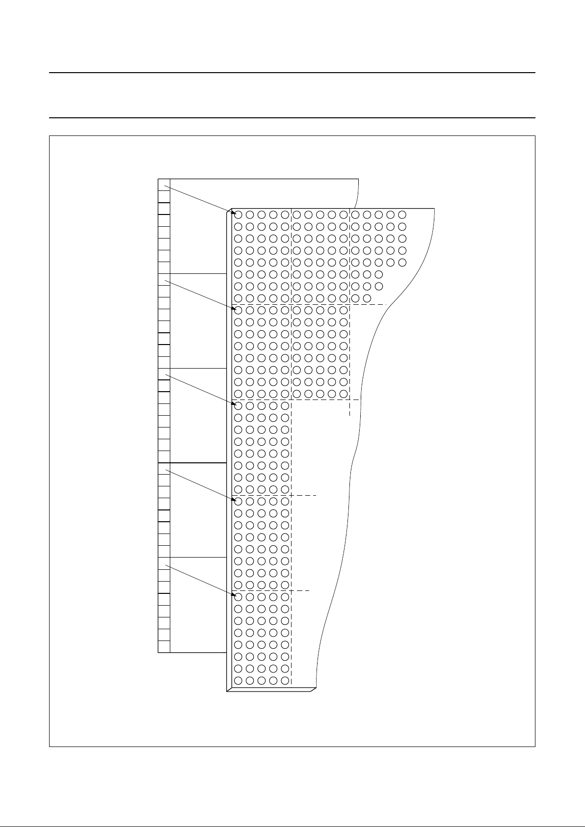
PCF8558
Fig.2 DDRAM to display mapping.
top of LCD
MGG559
RAM
bank 0
bank 1
bank 2
bank 3
bank 4
LCD
Page 7
1998 Apr 07 7
Philips Semiconductors Objective specification
Universal LCD driver for small graphic
panels
PCF8558
Fig.3 Typical LCD driver waveforms (MUX rate 1 : 40).
V
state1
(t)
=C2
(t)
− R1
(t)
; V
state2
(t)
=C2
(t)
− R2
(t)
.
MGG560
ROW 1
R1 (t)
ROW 2
R2 (t)
COL 1
C1 (t)
COL 2
C2 (t)
0 V
V
DD
V
2
V
3
V
4
V
5
V
LCD
V
DD
V
2
V
3
V
4
V
5
V
LCD
V
DD
V
2
V
3
V
4
V
5
V
LCD
V
DD
V
2
V
3
V
4
V
5
V
LCD
0.2731V
OP
0.2731V
OP
0.7269V
OP
0.7269V
OP
V
OP
V
OP
0 V
0.2731V
OP
0.2731V
OP
0.7269V
OP
0.7269V
OP
V
OP
V
OP
frame n frame n + 1
123456789 123456789
... 40 ... 40
V
state 1
(t)
V
state 2
(t)
V
state 1
(t)
V
state 2
(t)
Page 8
1998 Apr 07 8
Philips Semiconductors Objective specification
Universal LCD driver for small graphic
panels
PCF8558
ADDRESSING
The data is downloaded into the matrix of the PCF8558 as indicated in Figs 4 and 5.
The display RAM has a matrix of 40 by 101 bits (5 by 101 bytes). The columns are addressed by the address pointer.
After writing one byte the pointer is set to the next byte. Control of address increment, horizontal or vertical, is by bit V in
the command byte.
DATA STRUCTURE
Fig.4 RAM format, addressing.
handbook, full pagewidth
MGG561
display line 0 to 7
display line 8 to 15
display line 16 to 23
address 2
address 1
address 0
display line 24 to 31
display line 32 to 39
000
LSB
MSB
001
010 Y address
011
100
X
address 98
address 99
address 100
Fig.5 Order of writing data bytes into RAM.
handbook, full pagewidth
05
16
27
38
49
MGG562
0
101
202
303
404
1
102
203
304
405
2
103
204
305
406
. . .
. . .
. . .
. . .
. . .
a. Order of writing data bytes into RAM (V =1). b. Order of writing data bytes into RAM (V =0).
Page 9

1998 Apr 07 9
Philips Semiconductors Objective specification
Universal LCD driver for small graphic
panels
PCF8558
I2C-BUS PROTOCOL
Two 7-bit slave addresses (0111100 and 0111101) are
reserved for both the PCF8558. The least-significant bit of
the slave address is set by connecting input SA0 to
either 0 (VSS) or 1 (VDD). Therefore, two PCF8558 can be
used on the same I2C-bus allowing displays of up to
80 × 101 or 40 × 202 dots to be driven.
The I2C-bus protocol is shown in Fig.6.
All communications are initiated with a START condition
(S) from the I2C-bus master, which is followed by the
desired slave address and write bit. All devices with this
slave address acknowledge in parallel. All other devices
ignore the bus transfer.
In write mode (indicated by setting the read/write bit LOW)
one or more commands follow the slave address
acknowledgement. The commands are also
acknowledged by all addressed devices on the bus.
The last command must clear the continuation bit C. After
the last command a series of data bytes may follow.
The acknowledgement after each byte is made only by the
addressed device. After the last data byte has been
acknowledged, the I2C-bus master issues a STOP
condition (P).
For PCF8558, no read mode is provided.
Display bytes are written into the RAM at the address
specified by the data pointer and subaddress counter.
Both the data pointer and subaddress counter are
automatically incremented, enabling a stream of data to be
transferred to the DDRAM.
The instruction format is composed of I
2
C-bus slave
address followed by one command byte, one X address
pointer, followed by any number of data bytes.
Command execution/storing of data takes place during the
acknowledge cycle.
Definitions
• Transmitter: the device which sends the data to the bus
• Receiver: the device which receives the data from the
bus
• Master: the device which initiates a transfer, generates
clock signals and terminates a transfer
• Slave: the device addressed by a master
• Multi-master: more than one master can attempt to
control the bus at the same time. The I
2
C-bus can
accommodate this without data los/contention.
• Arbitration: procedure to ensure that, if more than one
master simultaneously tries to control the bus, only one
is allowed to do so and the message is not corrupted
• Synchronization: procedure to synchronize the clock
signals of two or more devices.
Fig.6 I2C-bus protocol.
handbook, full pagewidth
MGG563
S
A
O
S 011110
COMMAND
slave address
X ADDRESS
A
C
K
A
C
K
A
C
K
A
C
K
DISPLAY DATA
P
R/W
N ≥ 0 bytes
Page 10

1998 Apr 07 10
Philips Semiconductors Objective specification
Universal LCD driver for small graphic
panels
PCF8558
COMMANDS
Display Control
Table 2 Display status
PD: P
OWER-DOWN
• All LCD outputs at VDD (display off)
• Bias generator off
• Power-on reset on, oscillator off (external clock still
possible)
• V
LCD
can be disconnected
• I2C-bus, RAM, commands, etc. still function in
power-down mode.
Set Address
Table 3 Y0, Y1 and Y2 define the Y address vector
address of the display RAM
BIT LOGIC 0 LOGIC 1
PD normal power-down
V horizontal addressing vertical addressing
DISPLAY STATUS
BITS
ED
Blank 0 0
Normal 1 1
All segments on 1 0
Inverse video 0 1
Y2 Y1 Y0 LINE
0000
0011
0102
0113
1004
Set X address
The X address points to the columns. The range of X is
0 to 100 (64H).
Reset function
After power-on the chip has the following state:
• Power-down mode (PD = 1)
• RAM undefined
• RAM X and Y address undefined
• Display control bits (except PD) undefined
• I
2
C-bus interface reset.
Note
If the chip is used with an external clock source, after
power-on, the chip requires at least 2 clock pulses to
ensure that an internal synchronous reset is carried out.
After the internal reset, the chip goes into power-down
mode (PD = 1). If the clock pulses are not supplied, and
the reset is not cleared, the chip cannot respond to
commands in the I2C bus.
In applications where the internal oscillator is used
(pin OSC = VDD), the oscillator starts after power-on.
As soon as the synchronous reset is cleared, the chip goes
into power-down mode, and the oscillator is stopped.
Table 4 Instructions: control byte, address
INSTRUCTION DB7 DB6 DB5 DB4 DB3 DB2 DB1 DB0 DESCRIPTION
Display control 0 E D PD V Y2 Y1 Y0 Y address vector, display control
X address 0 X address set column address
Page 11

1998 Apr 07 11
Philips Semiconductors Objective specification
Universal LCD driver for small graphic
panels
PCF8558
CHARACTERISTICS OF THE I2C-BUS
The I2C-bus is for bidirectional, two-line communication
between different ICs or modules. The two lines are a
serial data line (SDA) and a serial clock line (SCL) which
must be connected to a positive supply via a pull-up
resistor. Data transfer may be initiated only when the bus
is not busy.
Bit transfer
One data bit is transferred during each clock pulse.
The data on the SDA line must remain stable during the
HIGH period of the clock pulse as changes in the data line
at this moment will be interpreted as control signals.
START and STOP conditions
Both data and clock lines remain HIGH when the bus is not
busy. A HIGH-to-LOW transition of the data line, while the
clock is HIGH, is defined as the START condition (S).
A LOW-to-HIGH transition of the data line while the clock
is HIGH, is defined as the STOP condition (P).
System configuration
A device transmitting a message is a 'transmitter', a device
receiving a message is the 'receiver'. The device that
controls the message flow is the 'master' and the devices
which are controlled by the master are the 'slaves'.
Acknowledge
The number of data bytes transferred between the START
and STOP conditions from transmitter to receiver is
unlimited. Each data byte of eight bits is followed by one
acknowledge bit. The acknowledge bit is a HIGH level put
on the bus by the transmitter, whereas the master
generates an extra acknowledge related clock pulse.
A slave receiver which is addressed must generate an
acknowledge after the reception of each byte. Also a
master must generate an acknowledge after the reception
of each byte that has been clocked out of the slave
transmitter. The device that acknowledges must pull down
the SDA line during the acknowledge clock pulse, so that
the SDA line is stable LOW during the HIGH period of the
acknowledge related clock pulse (set-up and hold times
must be taken into consideration). A master receiver must
signal the end of a data transmission to the transmitter by
not generating an acknowledge on the last byte that has
been clocked out of the slave. In this event the transmitter
must leave the data line HIGH to enable the master to
generate a stop condition.
Fig.7 Bit transfer.
andbook, full pagewidth
MBC621
data line
stable;
data valid
change
of data
allowed
SDA
SCL
Page 12

1998 Apr 07 12
Philips Semiconductors Objective specification
Universal LCD driver for small graphic
panels
PCF8558
Fig.8 Definition of START and STOP condition.
handbook, full pagewidth
MBC622
SDA
SCL
P
STOP condition
SDA
SCL
S
START condition
Fig.9 System configuration.
MGA807
SDA
SCL
MASTER
TRANSMITTER/
RECEIVER
MASTER
TRANSMITTER
SLAVE
TRANSMITTER/
RECEIVER
SLAVE
RECEIVER
MASTER
TRANSMITTER/
RECEIVER
Page 13

1998 Apr 07 13
Philips Semiconductors Objective specification
Universal LCD driver for small graphic
panels
PCF8558
The general characteristics and detailed specification of the I2C-bus are available on request (order number 9398 39340011).
handbook, full pagewidth
MBC602
S
START
condition
9821
clock pulse for
acknowledgement
not acknowledge
acknowledge
DATA OUTPUT
BY TRANSMITTER
DATA OUTPUT
BY RECEIVER
SCL FROM
MASTER
Fig.10 Acknowledgment on the I2C-bus.
LIMITING VALUES
In accordance with the Absolute Maximum Rating System (IEC 134).
HANDLING
Inputs and outputs are protected against electrostatic discharge in normal handling. However, to be totally safe it is
desirable to take normal precautions appropriate to handling MOS devices.
SYMBOL PARAMETER MIN. MAX. UNIT
V
DD
supply voltage −0.5 +8.0 V
V
LCD
LCD supply voltage VDD− 11 V
DD
V
V
i1
input voltage T1, T3, SA0 and OSC VSS− 0.5 VDD+ 0.5 V
V
i2
input voltage SDA and SCL VSS− 0.5 8.0 V
V
o1
output voltage T2 and SDA VSS− 0.5 VDD+ 0.5 V
V
o2
output voltage R1 to R40 and C1 to C101 V
LCD
− 0.5 VDD+ 0.5 V
I
I
DC input current −10 +10 mA
I
O
DC output current −10 +10 mA
I
DD
, ISS, I
LCD
VDD, VSS or V
LCD
current −50 +50 mA
P
tot
power dissipation per package − 400 mW
P
o
power dissipation per output − 100 mW
T
stg
storage temperature −65 +150 °C
Page 14

1998 Apr 07 14
Philips Semiconductors Objective specification
Universal LCD driver for small graphic
panels
PCF8558
DC CHARACTERISTICS
V
DD
= 2.5 to 6 V; VSS=0V; V
LCD=VDD
− 3.5 V to VDD− 9 V; T
amb
= −40 to +85 °C; unless otherwise specified, note 1.
Notes
1. Outputs are open-circuit; inputs at V
DD
or VSS; I2C-bus inactive; external clock with 50% duty factor.
2. Resets all logic when VDD<V
POR
.
3. Periodically sampled, not 100% tested.
4. Resistance of output terminals (R1 to R40 and C1 to C101) with IL=20µA; VOP=VDD− V
LCD
= 9 V; outputs
measured one at a time.
5. When the voltages are above or below the supply voltages VDD or VSS, an input current may flow. This current must
not exceed ±0.5 mA.
SYMBOL PARAMETER CONDITIONS MIN. TYP. MAX. UNIT
Supplies
V
DD
supply voltage 2.5 − 6.0 V
V
LCD
LCD supply voltage VDD− 9 − VDD− 3.5 V
I
DD(PD)
supply current in power-down mode − 510µA
I
DD1
supply current external clock − 120 180 µA
I
DD2
supply current internal clock − 130 200 µA
I
LCD
LCD input current − 50 100 µA
V
POR
power-on reset level note 2 0.6 1.3 1.8 V
Logic
V
IL1
LOW level input voltage (all inputs
except OSC)
V
SS
− 0.3V
DD
V
V
IH1
HIGH level input voltage (all inputs
except OSC)
0.7V
DD
− V
DD
V
V
IL2
LOW level input voltage (pin OSC) V
SS
− VDD− 1.5 V
V
IH2
HIGH level input voltage (pin OSC) VDD− 0.1 − V
DD
V
I
L1
leakage current at T1, T3 OSC and SA0 VI=VDD or V
SS
−1 − +1 mA
C
I1
input capacitance at T1, T3 OSC and
SA0
note 3 −−5pF
LCD outputs
V
DC
DC component of LCD drivers R1 to R40
and C1 to C101
−±20 − mV
R
ROW
output resistance R1 to R40 note 4 − 1.5 6 kΩ
R
COL
output resistance C1 to C101 note 4 − 310kΩ
I
2
C-bus; SDA and SCL
V
IL3
LOW level input voltage note 5 V
SS
− 0.3V
DD
V
V
IH3
HIGH level input voltage note 5 0.7V
DD
− 6V
I
L2
leakage current VI=VDDor V
SS
−1 − +1 mA
C
I2
input capacitance note 3 −−7pF
I
OL
LOW level output current at SDA VOL= 0.4 V;
VDD=5V
3.0 −−mA
Page 15

1998 Apr 07 15
Philips Semiconductors Objective specification
Universal LCD driver for small graphic
panels
PCF8558
AC CHARACTERISTICS
All timing values are referenced to V
IH
and VIL levels with an input voltage swing of VSSto VDD. VDD= 2.5 to 6 V;
V
SS
=0V;V
LCD=VDD
− 3.5VtoVDD− 9V;T
amb
= −40 to +85 °C; unless otherwise specified.
Notes
1. The rise and fall times specified here refer to the driver device (i.e. not PCF8558) and are part of the general fast
I
2
C-bus specification. However, when PCF8558 asserts an acknowledge on SDA, the fall time is given by parameter
tf. Cb= capacitive load per bus line.
2. The device inputs SDA and SCL are filtered and will reject spikes on the bus lines of width <t
SW(max)
.
SYMBOL PARAMETER CONDITIONS MIN. TYP. MAX. UNIT
f
FR)
LCD frame frequency
(internal oscillator)
37 62.5 94 Hz
f
OSC(ext)
external clock frequency 90 150 225 kHz
t
PLCD
driver delays VDD− V
LCD
=9V;
with test loads
−−100 µs
I
2
C-bus (see Fig.12)
f
SCL
SCL clock frequency −−400 kHz
t
CLKL
SCL LOW time 1.3 −−µs
t
CLKH
SCL HIGH time 0.6 −−µs
t
BUF
bus free time between successive STOP
and START conditions
1.3 −−µs
t
r
SCL and SDA rise time note 1 −−300 ns
t
f
SCL and SDA fall time note 1 20 + 0.1Cb− 300 ns
t
SU;STA
START condition set-up time repeated start codes only 0.6 −−µs
t
HD;STA
START condition hold time 0.6 −−µs
t
SU;DAT
data set-up time 100 −−ns
t
HD;DAT
data hold time 0 −−ns
t
SU;STO
STOP condition set-up time 0.6 −−µs
t
SW
tolerable spike width on bus note 2 −−50 ns
C
b
capacitive load per bus line −−400 pF
Fig.11 AC test loads.
handbook, full pagewidth
MGG564
1.5 kΩ
V
DD
SDA
1 nF
R1 to R40,
C1 to C101
Page 16

1998 Apr 07 16
Philips Semiconductors Objective specification
Universal LCD driver for small graphic
panels
PCF8558
Fig.12 I2C-bus timing waveforms.
dbook, full pagewidth
SDA
MGA728
SDA
SCL
t
SU;STA
t
SU;STO
t
HD;STA
t
BUF
t
LOW
t
HD;DAT
t
HIGH
t
r
t
f
t
SU;DAT
Page 17

1998 Apr 07 17
Philips Semiconductors Objective specification
Universal LCD driver for small graphic
panels
PCF8558
APPLICATION INFORMATION
The pinning of the PCF8558 is optimized for single plane wiring e.g. for Chip-on-glass display modules.
Fig.13 Application using I2C-bus interface.
handbook, full pagewidth
MGG565
OSC
V
DD
V
LCD
V
SS
SCL SDA
SA0
100 nF
100
nF
40
101
40 × 101 dots
full graphic display
R1 to R40
C1 to C101
V
DD
V
LCD
V
SS
V
DD
V
DD
V
DD
PCF8558
SCL SDA
MASTER TRANSMITTER
PCF84C81A; P80CL410
OSC
V
DD
V
LCD
V
SS
SCL SDA
SA0
100 nF
100
nF
40
101
40 × 101 dots
full graphic display
R1 to R40
C1 to C101
V
DD
V
LCD
V
SS
V
SS
PCF8558
Page 18

1998 Apr 07 18
Philips Semiconductors Objective specification
Universal LCD driver for small graphic
panels
PCF8558
CHIP INFORMATION
The PCF8558 is manufactured in p-well CMOS
technology. VDD− V
LCD
is positive. The chip substrate is
connected to VDD.
Bonding pads
Pad pitch 100 µm
Pad size, aluminium 80 × 120 µm
Bump dimensions 59 × 99 × 15 µm
Wafer thickness 381 µm
Fig.14 Application, display size 40 × 101 pixels.
handbook, halfpage
MGG566
DISPLAY 40 × 101
PCF8558
supply, I/O
8
101 2020
Fig.15 Bonding pads.
handbook, halfpage
MGG567
4 mm
pitch
PCF8558
9 mm
Y
X
Page 19

1998 Apr 07 19
Philips Semiconductors Objective specification
Universal LCD driver for small graphic
panels
PCF8558
BONDING PAD LOCATIONS
Fig.16 Bonding pad locations.
handbook, full pagewidth
MGG568
R32
R21
C1
C17
R33
R40
C18
C95
V
DD
T3
V
LCD
V
SS
SCL
R20
C101
R8R1R7
C96
Y
X
OSC
SA0
T1
SDA
T2
PCF8558
~3.99 mm
~8.95
mm
dummy 1
dummy 6
x
y
0
0
Page 20

1998 Apr 07 20
Philips Semiconductors Objective specification
Universal LCD driver for small graphic
panels
PCF8558
Table 5 Bonding pad locations (dimensions in µm).
All x/y coordinates are referenced to the centre
of the chip, see Fig.16.
SYMBOL PAD x y
SCL 1 −4303.6 1280.0
R20 2 −4303.6 1005.8
R19 3 −4303.6 905.8
R18 4 −4303.6 805.8
R17 5 −4303.6 705.8
R16 6 −4303.6 605.8
R15 7 −4303.6 505.8
R14 8 −4303.6 405.8
R13 9 −4303.6 305.8
R12 10 −4303.6 205.8
R11 11 −4303.6 105.8
R10 12 −4303.6 5.8
R9 13 −4303.6 −94.3
R8 14 −4303.6 −194.3
R7 15 −4303.6 −383.3
R6 16 −4303.6 −483.3
R5 17 −4303.6 −583.3
R4 18 −4303.6 −683.3
R3 19 −4303.6 −783.3
R2 20 −4303.6 −883.3
R1 21 −4303.6 −983.3
C101 22 −4303.6 −1083.3
C100 23 −4303.6 −1183.3
C99 24 −4303.6 −1283.3
C98 25 −4303.6 −1383.3
C97 26 −4303.6 −1483.3
C96 27 −4303.6 −1583.3
C95 28 −3903.6 −1823.5
C94 29 −3803.6 −1823.5
C93 30 −3703.6 −1823.5
C92 31 −3603.6 −1823.5
C91 32 −3503.6 −1823.5
C90 33 −3403.6 −1823.5
C89 34 −3303.6 −1823.5
C88 35 −3203.6 −1823.5
C87 36 −3103.6 −1823.5
C86 37 −3003.6 −1823.5
C85 38 −2903.6 −1823.5
C84 39 −2803.6 −1823.5
C83 40 −2703.6 −1823.5
C82 41 −2603.6 −1823.5
C81 42 −2503.6 −1823.5
C80 43 −2403.6 −1823.5
C79 44 −2303.6 −1823.5
C78 45 −2203.6 −1823.5
C77 46 −2103.6 −1823.5
C76 47 −2003.6 −1823.5
C75 48 −1814.6 −1823.5
C74 49 −1714.6 −1823.5
C73 50 −1614.6 −1823.5
C72 51 −1514.6 −1823.5
C71 52 −1414.6 −1823.5
C70 53 −1314.6 −1823.5
C69 54 −1214.6 −1823.5
C68 55 −1114.6 −1823.5
C67 56 −1014.6 −1823.5
C66 57 −914.6 −1823.5
C65 58 −814.6 −1823.5
C64 59 −714.6 −1823.5
C63 60 −614.6 −1823.5
C62 61 −514.6 −1823.5
C61 62 −414.6 −1823.5
C60 63 −314.6 −1823.5
C59 64 −214.6 −1823.5
C58 65 −114.6 −1823.5
C57 66 −14.6 −1823.5
C56 67 85.4 −1823.5
C55 68 274.4 −1823.5
C54 69 374.4 −1823.5
C53 70 474.4 −1823.5
C52 71 574.4 −1823.5
C51 72 674.4 −1823.5
C50 73 774.4 −1823.5
C49 74 874.4 −1823.5
C48 75 974.4 −1823.5
C47 76 1074.4 −1823.5
C46 77 1174.4 −1823.5
C45 78 1274.4 −1823.5
C44 79 1374.4 −1823.5
C43 80 1474.4 −1823.5
C42 81 1574.4 −1823.5
C41 82 1674.4 −1823.5
SYMBOL PAD x y
Page 21

1998 Apr 07 21
Philips Semiconductors Objective specification
Universal LCD driver for small graphic
panels
PCF8558
C40 83 1774.4 −1823.5
C39 84 1874.4 −1823.5
C38 85 1974.4 −1823.5
C37 86 2074.4 −1823.5
C36 87 2174.4 −1823.5
C35 88 2363.4 −1823.5
C34 89 2463.4 −1823.5
C33 90 2563.4 −1823.5
C32 91 2663.4 −1823.5
C31 92 2763.4 −1823.5
C30 93 2863.4 −1823.5
C29 94 2963.4 −1823.5
C28 95 3063.4 −1823.5
C27 96 3163.4 −1823.5
C26 97 3263.4 −1823.5
C25 98 3363.4 −1823.5
C24 99 3463.4 −1823.5
C23 100 3563.4 −1823.5
C22 101 3663.4 −1823.5
C21 102 3763.4 −1823.5
C20 103 3863.4 −1823.5
C19 104 3963.4 −1823.5
C18 105 4063.4 −1823.5
C17 106 4303.6 −1583
C16 107 4303.6 −1483
C15 108 4303.6 −1383
C14 109 4303.6 −1283
C13 110 4303.6 −1183
C12 111 4303.6 −1083
C11 112 4303.6 −983
C10 113 4303.6 −883
C9 114 4303.6 −783
C8 115 4303.6 −683
C7 116 4303.6 −583
C6 117 4303.6 −483
C5 118 4303.6 −383
C4 119 4303.6 −283
C3 120 4303.6 −183
C2 121 4303.6 5.8
C1 122 4303.6 105.8
R21 123 4303.6 483
R22 124 4303.6 583
R23 125 4303.6 683
R24 126 4303.6 783
SYMBOL PAD x y
R25 127 4303.6 883
R26 128 4303.6 983
R27 129 4303.6 1083
R28 130 4303.6 1183
R29 131 4303.6 1283
R30 132 4303.6 1383
R31 133 4303.6 1483
R32 134 4303.6 1583
R33 135 4017.1 1823.5
R34 136 3917.1 1823.5
R35 137 3817.1 1823.5
R36 138 3717.1 1823.5
R37 139 3617.1 1823.5
R38 140 3517.1 1823.5
R39 141 3417.1 1823.5
R40 142 3317.1 1823.5
T2 143 −2695.6 1823.5
SDA 144 −3044.1 1823.5
V
SS
145 −3190.6 1823.5
T1 146 −3362.1 1823.5
V
LCD
147 −3463.6 1823.5
SA0 148 −3635.1 1823.5
T3 149 −3735.1 1823.5
OSC 150 −3839.1 1823.5
V
DD
151 −3939.6 1823.5
Dummy pads
dummy 1 −−257.1 1790.4
dummy 2 −−155.6 1790.4
dummy 3 −−54.1 1790.4
dummy 4 − 47.4 1790.4
dummy 5 − 148.9 1790.4
dummy 6 − 250.4 1790.4
dummy 7 −−4223.6 1823.4
dummy 8 − 4303.5 1843.5
dummy 9 −−4303.6 −1843.5
dummy 10 − 4323.6 −1843.5
Alignment marks
Sign C −−4082.6 −1782.5
Sign C − 4147.4 1807.5
Sign F −−4262.6 1417.5
SYMBOL PAD x y
Page 22

1998 Apr 07 22
Philips Semiconductors Objective specification
Universal LCD driver for small graphic
panels
PCF8558
DEFINITIONS
LIFE SUPPORT APPLICATIONS
These products are not designed for use in life support appliances, devices, or systems where malfunction of these
products can reasonably be expected to result in personal injury. Philips customers using or selling these products for
use in such applications do so at their own risk and agree to fully indemnify Philips for any damages resulting from such
improper use or sale.
PURCHASE OF PHILIPS I
2
C COMPONENTS
Data sheet status
Objective specification This data sheet contains target or goal specifications for product development.
Preliminary specification This data sheet contains preliminary data; supplementary data may be published later.
Product specification This data sheet contains final product specifications.
Limiting values
Limiting values given are in accordance with the Absolute Maximum Rating System (IEC 134). Stress above one or
more of the limiting values may cause permanent damage to the device. These are stress ratings only and operation
of the device at these or at any other conditions above those given in the Characteristics sections of the specification
is not implied. Exposure to limiting values for extended periods may affect device reliability.
Application information
Where application information is given, it is advisory and does not form part of the specification.
Purchase of Philips I
2
C components conveys a license under the Philips’ I2C patent to use the
components in the I2C system provided the system conforms to the I2C specification defined by
Philips. This specification can be ordered using the code 9398 393 40011.
Page 23

1998 Apr 07 23
Philips Semiconductors Objective specification
Universal LCD driver for small graphic
panels
PCF8558
NOTES
Page 24

Internet: http://www.semiconductors.philips.com
Philips Semiconductors – a worldwide company
© Philips Electronics N.V. 1998 SCA59
All rights are reserved. Reproduction in whole or in part is prohibited without the prior written consent of the copyright owner.
The information presented in this document does not form part of any quotation or contract, is believed to be accurate and reliable and may be changed
without notice. No liability will be accepted by the publisher for any consequence of its use. Publication thereof does not convey nor imply any license
under patent- or other industrial or intellectual property rights.
Middle East: see Italy
Netherlands: Postbus 90050, 5600PB EINDHOVEN, Bldg. VB,
Tel. +31 40 27 82785, Fax. +31 40 27 88399
New Zealand: 2 Wagener Place, C.P.O. Box 1041, AUCKLAND,
Tel. +64 9 849 4160, Fax. +64 9 849 7811
Norway: Box 1, Manglerud 0612, OSLO,
Tel. +47 22 74 8000, Fax. +47 22 74 8341
Pakistan: see Singapore
Philippines: Philips Semiconductors Philippines Inc.,
106 Valero St. Salcedo Village, P.O. Box 2108 MCC, MAKATI,
Metro MANILA, Tel. +63 2 816 6380, Fax. +63 2 817 3474
Poland: Ul. Lukiska 10, PL 04-123 WARSZAWA,
Tel. +48 22 612 2831, Fax. +48 22 612 2327
Portugal: see Spain
Romania: see Italy
Russia: Philips Russia, Ul. Usatcheva 35A, 119048 MOSCOW,
Tel. +7 095 755 6918, Fax. +7 095 755 6919
Singapore: Lorong 1, Toa Payoh, SINGAPORE 319762,
Tel. +65 350 2538, Fax. +65 251 6500
Slovakia: see Austria
Slovenia: see Italy
South Africa: S.A. PHILIPS Pty Ltd., 195-215 Main Road Martindale,
2092 JOHANNESBURG, P.O. Box 7430 Johannesburg 2000,
Tel. +27 11 470 5911, Fax. +27 11 470 5494
South America: Al. Vicente Pinzon, 173, 6th floor,
04547-130 SÃO PAULO, SP, Brazil,
Tel. +55 11 821 2333, Fax. +55 11 821 2382
Spain: Balmes 22, 08007 BARCELONA,
Tel. +34 3 301 6312, Fax. +34 3 301 4107
Sweden: Kottbygatan 7, Akalla, S-16485 STOCKHOLM,
Tel. +46 8 5985 2000, Fax. +46 8 5985 2745
Switzerland: Allmendstrasse 140, CH-8027 ZÜRICH,
Tel. +41 1 488 2741 Fax. +41 1 488 3263
Taiwan: Philips Semiconductors, 6F, No. 96, Chien Kuo N. Rd., Sec. 1,
TAIPEI, Taiwan Tel. +886 2 2134 2865, Fax. +886 2 2134 2874
Thailand: PHILIPS ELECTRONICS (THAILAND) Ltd.,
209/2 Sanpavuth-Bangna Road Prakanong, BANGKOK 10260,
Tel. +66 2 745 4090, Fax. +66 2 398 0793
Turkey: Talatpasa Cad. No. 5, 80640 GÜLTEPE/ISTANBUL,
Tel. +90 212 279 2770, Fax. +90 212 282 6707
Ukraine: PHILIPS UKRAINE, 4 Patrice Lumumba str., Building B, Floor 7,
252042 KIEV, Tel. +380 44 264 2776, Fax. +380 44 268 0461
United Kingdom: Philips Semiconductors Ltd., 276 Bath Road, Hayes,
MIDDLESEX UB3 5BX, Tel. +44 181 730 5000, Fax. +44 181 754 8421
United States: 811 East Arques Avenue, SUNNYVALE, CA 94088-3409,
Tel. +1 800 234 7381
Uruguay: see South America
Vietnam: see Singapore
Yugoslavia: PHILIPS, Trg N. Pasica 5/v, 11000 BEOGRAD,
Tel. +381 11 625 344, Fax.+381 11 635 777
For all other countries apply to: Philips Semiconductors,
International Marketing & Sales Communications, Building BE-p, P.O. Box 218,
5600 MD EINDHOVEN, The Netherlands, Fax. +31 40 27 24825
Argentina: see South America
Australia: 34 Waterloo Road, NORTH RYDE, NSW 2113,
Tel. +61 2 9805 4455, Fax. +61 2 9805 4466
Austria: Computerstr. 6, A-1101 WIEN, P.O. Box 213, Tel. +43 160 1010,
Fax. +43 160 101 1210
Belarus: Hotel Minsk Business Center, Bld. 3, r. 1211, Volodarski Str. 6,
220050 MINSK, Tel. +375 172 200 733, Fax. +375 172 200 773
Belgium: see The Netherlands
Brazil: seeSouth America
Bulgaria: Philips Bulgaria Ltd., Energoproject, 15thfloor,
51 James Bourchier Blvd., 1407 SOFIA,
Tel. +359 2 689 211, Fax. +359 2 689 102
Canada: PHILIPS SEMICONDUCTORS/COMPONENTS,
Tel. +1 800 234 7381
China/Hong Kong: 501 Hong Kong Industrial Technology Centre,
72 Tat Chee Avenue, Kowloon Tong, HONG KONG,
Tel. +852 2319 7888, Fax. +852 2319 7700
Colombia: see South America
Czech Republic: see Austria
Denmark: Prags Boulevard 80, PB 1919, DK-2300 COPENHAGEN S,
Tel. +45 32 88 2636, Fax. +45 31 57 0044
Finland: Sinikalliontie 3, FIN-02630 ESPOO,
Tel. +358 9 615800, Fax. +358 9 61580920
France: 51 Rue Carnot, BP317, 92156 SURESNES Cedex,
Tel. +33 1 40 99 6161, Fax. +33 1 40 99 6427
Germany: Hammerbrookstraße 69, D-20097 HAMBURG,
Tel. +49 40 23 53 60, Fax. +49 40 23 536 300
Greece: No. 15, 25th March Street, GR 17778 TAVROS/ATHENS,
Tel. +30 1 4894 339/239, Fax. +30 1 4814 240
Hungary: seeAustria
India: Philips INDIA Ltd, Band Box Building, 2nd floor,
254-D, Dr. Annie Besant Road, Worli, MUMBAI 400 025,
Tel. +91 22 493 8541, Fax. +91 22 493 0966
Indonesia: PT Philips Development Corporation, Semiconductors Division,
Gedung Philips, Jl. Buncit Raya Kav.99-100, JAKARTA 12510,
Tel. +62 21 794 0040 ext. 2501, Fax. +62 21 794 0080
Ireland: Newstead, Clonskeagh, DUBLIN 14,
Tel. +353 1 7640 000, Fax. +353 1 7640 200
Israel: RAPAC Electronics, 7 Kehilat Saloniki St, PO Box 18053,
TEL AVIV 61180, Tel. +972 3 645 0444, Fax. +972 3 649 1007
Italy: PHILIPS SEMICONDUCTORS, Piazza IV Novembre 3,
20124 MILANO, Tel. +39 2 6752 2531, Fax. +39 2 6752 2557
Japan: Philips Bldg 13-37, Kohnan 2-chome, Minato-ku, TOKYO 108,
Tel. +81 3 3740 5130, Fax. +81 3 3740 5077
Korea: Philips House, 260-199 Itaewon-dong, Yongsan-ku, SEOUL,
Tel. +82 2 709 1412, Fax. +82 2 709 1415
Malaysia: No. 76 Jalan Universiti, 46200 PETALING JAYA, SELANGOR,
Tel. +60 3 750 5214, Fax. +60 3 757 4880
Mexico: 5900 Gateway East, Suite 200, EL PASO, TEXAS 79905,
Tel. +9-5 800 234 7381
Printed in The Netherlands 415106/1200/02/pp24 Date of release: 1998 Apr 07 Document order number: 9397 750 03284
 Loading...