

Page 1

INTEGRATED CIRCUITS
DATA SH EET
PCF8549
65 × 102 pixels matrix LCD driver
Product specification
File under Integrated Circuits, IC12
1997 Nov 21
Page 2

Philips Semiconductors Product specification
65 × 102 pixels matrix LCD driver PCF8549
FEATURES
• Single chip LCD controller/driver
• 65 row and 102 column outputs
• Display data RAM 65 × 102 bits
• On-chip:
– Generation of LCD supply voltage
– Generation of intermediate LCD bias voltages
– Oscillator requires no external components (external
clock also possible)
• 400 kHz Fast I2C Interface
• CMOS compatible inputs
• Mux rate: 65
• Logic supply voltage range V
• Voltage generator voltage range V
− VSS: 1.5 to 6 V
DD1
DD2/2_HV
− VSS:
2.4 to 5 V
• Display supply voltage range V
− VSS: 7.0 to 16 V
LCD
• Low power consumption, suitable for battery operated
systems
• Temperature compensation of V
LCD
• Interlacing for better display quality
• Slim chip layout, suited for chip-on-glass applications.
GENERAL DESCRIPTION
The PCF8549 is a low power CMOS LCD controller driver,
designed to drive a graphic display of 65 rows and
102 columns. All necessary functions for the display are
provided in a single chip, including on-chip generation of
LCD supply and bias voltages, resulting in a minimum of
external components and low power consumption. The
PCF8549 interfaces to most microcontrollers via an
I2C interface.
Packages
The PCF8549U/2 is available as bumped die. Sawn wafer
as chip sorted in chip tray. For further details see
Section “Bonding pads”.
Customized TCP upon request.
APPLICATIONS
• Telecom equipment
• Portable instruments
• Point of sale terminals.
ORDERING INFORMATION
TYPE NUMBER
NAME DESCRIPTION VERSION
PCF8549U/2/F1 TRAY chip with bumps in tray
PACKAGE
1997 Nov 21 2
Page 3

Philips Semiconductors Product specification
65 × 102 pixels matrix LCD driver PCF8549
BLOCK DIAGRAM
VLCD2
VLCD1
Bias voltage generator
HVGEN
7 stages
C0 to C101
COLUMN DRIVERS
DATA LATCHES
Dual Ported RAM
65x102 Bit
R0 to R64
ROW DRIVERS
SHIFT REGISTER
OSCILLATOR
TIMING GENERATOR
OSC
IIC INTERFACE
SDA_out
SDA
SCL
1997 Nov 21 3
SA0
RES
Fig.1 Block diagram.
T1
DISPLAY CONTROL LOGIC
T3
T4
T2
T5T6T7
VDD1
VDD2
VDD2_HV
VSS1
VSS2
VSS2_HV
Page 4
Philips Semiconductors Product specification
65 × 102 pixels matrix LCD driver PCF8549
PINNING
SYMBOL DESCRIPTION
R0 to R64 LCD row driver outputs
C0 to C101 LCD column driver outputs
V
SS1,2,2_HV
V
DD1,2,2_HV
V
LCD1,2
T1 test 1 input
T2 test 2 output
T3 test 3 I/O
T4 test 4 I/O
T5 test 5 input
T6 test 6 input
T7 test 7 input
SDA I
SCL I
SDA_OUT I
SA0 least significant bit of slave address
OSC oscillator
RES external reset input, low active
negative power supply
supply voltage
LCD supply voltage
2
C data input
2
C clock line
2
C output
Pin functions
R0 TO R64: ROW DRIVER OUTPUTS
These pads output the row signals.
TO C101: COLUMN DRIVER OUTPUTS
C0
These pads output the column signals.
V
SS1,2,2_HV
: NEGATIVE POWER SUPPLY RAILS
Negative power supplies.
V
DD1,2,2_HV
V
DD2
: POSITIVE POWER SUPPLY RAILS
and V
are the supply voltages for the internal voltage generator. Both have to be on the same voltage and
DD2_HV
may be connected together outside of the chip. If the internal voltage generator is not used, they should be both
connected to ground. V
V
DD2
V
LCD1,2
and V
: LCD POWER SUPPLY
DD2_HV
.
is used as power supply for the rest of the chip. This voltage can be a different voltage than
DD1
Positive power supply for the liquid crystal display. If the internal voltage generator is used, the two supply rails
V
LCD1
case, V
and V
LCD1
must be connected together. An external LCD supply voltage can be supplied using the V pad. In this
LCD2
has to be connected to ground, and the internal voltage generator has to be programmed to zero. If the
PCF8549 is in power-down mode, the external LCD supply voltage has to be switched off.
1997 Nov 21 4
Page 5

Philips Semiconductors Product specification
65 × 102 pixels matrix LCD driver PCF8549
T1, T2, T3, T4, T5, T6 AND T7: TEST PADS
T1, T3, T4, T5, T6 and T7 must be connected to V
SS1
, T2
is to be left open. Not accessible to user.
2
SDA/SDA_OUT: I
CDATA LINES
Output and input are separated. If both pads are
connected together they behave like a standard I2C pad.
2
SCL: I
C CLOCK SIGNAL
Input for the I2C-bus clock signal.
LAVE ADDRESS
SA0: S
With the SA0 pin two different slave addresses can be
selected. That allows to connect two PCF8549 LCD
drivers to the same I2C-bus.
OSCILLATOR
OSC:
When the on-chip oscillator is used this input must be
connected to V
. An external clock signal, if used, is
DD1
connected to this input.
RES: RESET
FUNCTIONAL DESCRIPTION
Block diagram functions
O
SCILLATOR
The on-chip oscillator provides the clock signal for the
display system. No external components are required and
the OSC input must be connected to V
. An external
DD1
clock signal, if used, is connected to this input.
2
CINTERFACE
I
The I2C interface receives and executes the commands
sent via the I2C-bus. It also receives RAM-data and sends
them to the RAM. During read access the 8-bit parallel
data or the status register content is converted to a serial
data stream and output via the I2C-bus.
D
ISPLAY CONTROL LOGIC
The display control logic generates the control signals to
read out the RAM via the 101 bit parallel port. It also
generates the control signals for the row, and
column drivers.
ISPLAY DATA RAM (DDRAM)
D
This signal will reset the device. Signal is active low.
The PCF8549 contains a 65 × 102 bit static RAM which
stores the display data. The RAM is divided into 8 banks of
102 bytes and one bank of 102 bits
((8 × 8+1)×102 bits). During RAM access, data is
transferred to the RAM via the I2C interface. There is a
direct correspondence between X-address and column
output number.
IMING GENERATOR
T
The timing generator produces the various signals
required to drive the internal circuitry. Internal chip
operation is not disturbed by operations on the I2C-bus.
LCD
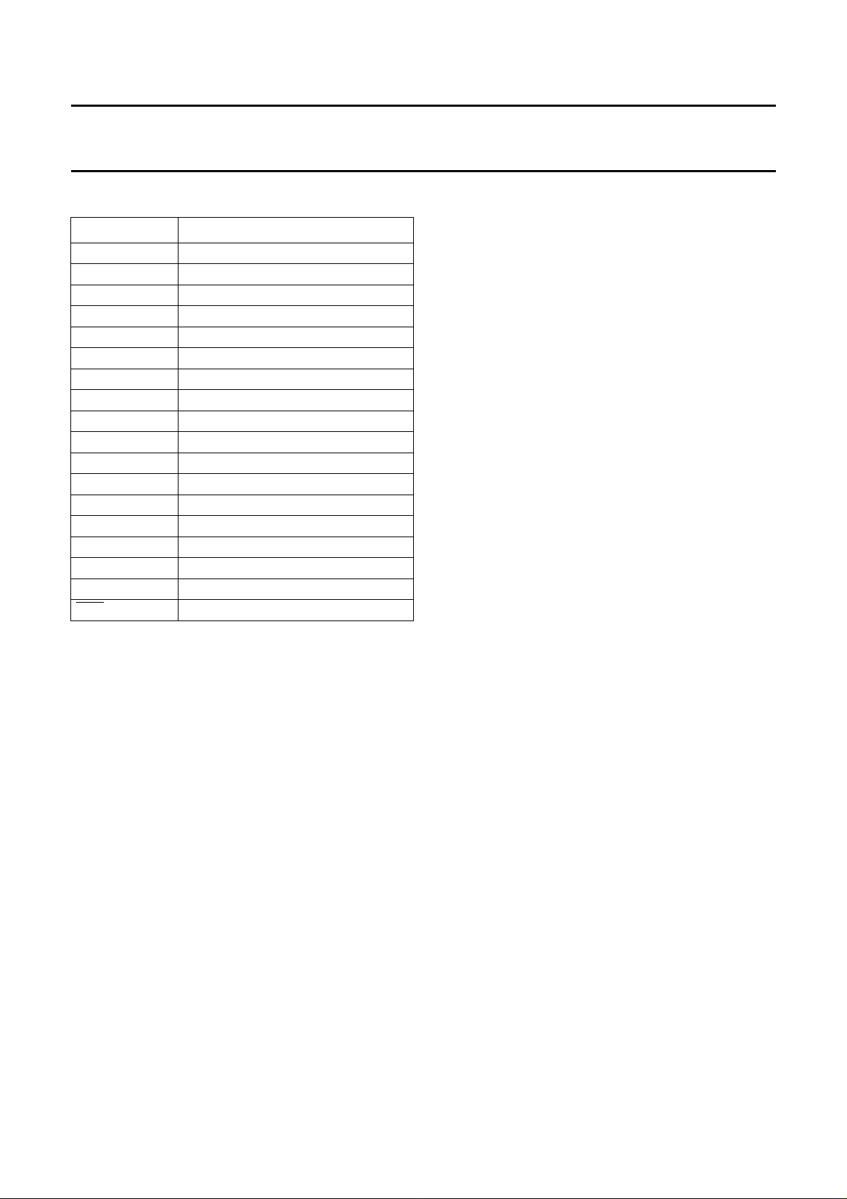
ROW AND COLUMN DRIVERS
The PCF8549 contains 65 row and 102 column drivers,
which connect the appropriate LCD bias voltages to the
display in accordance with the data to be displayed.
Figure 2 shows typical waveforms. Unused outputs should
be left unconnected.
1997 Nov 21 5
Page 6

Philips Semiconductors Product specification
65 × 102 pixels matrix LCD driver PCF8549
ROW 0
R0 (t)
ROW 2
R2 (t)
COL 0
C0 (t)
COL 1
C1 (t)
V
LCD
V
3
(t)
V
LCD
0 V
state1
V3 - V
V
V
LCD
V
3
- V
frame n+1frame n
V
LCD
V
2
V
3
V
4
V
5
V
SS
V
LCD
V
2
V
3
V
4
V
5
V
SS
V
LCD
V
2
V
3
V
4
V
5
V
SS
V
LCD
V
2
V
3
V
4
V
5
V
SS
2
2
V4 - V
0 V
V
5
V4 - V
- V
LCD
5
LCD
V
V
state1
state2
(t)
(t)
(t)
V
- V
LCD
2
0 V
state2
V3 - V
2
V
0 2 4 6 8 10 ...
0 2 4 6 8 10 ...
V
(t) = C1(t) - R0(t)
state1
V
(t) = C1(t) - R2(t)
state2
... 64
1 3 5 7 9 ...
... 63
Fig.2 Typical LCD driver waveforms.
1997 Nov 21 6
... 64
1 3 5 7 9 ...
... 63
V4 - V
0 V
V
5
V4 - V
- V
LCD
VSS=0V
5
LCD
Page 7

Philips Semiconductors Product specification
65 × 102 pixels matrix LCD driver PCF8549
DDRAM
bank 0
bank 1
bank 2
bank 3
bank 7
bank 8
Fig.3 DDRAM to display mapping.
1997 Nov 21 7
Page 8

Philips Semiconductors Product specification
65 × 102 pixels matrix LCD driver PCF8549
Addressing
The Display data RAM of the PCF8549 is accessed as
indicated in Figs 3, 4, 4, 6 and 7. The display RAM has a
matrix of 65 × 102 bits. The columns are addressed by the
address pointer. The address ranges are:
X 0 to 101 (1100101b) and Y 0 to 8 (1000b). Addresses
outside these ranges are not allowed. In vertical
addressing mode (V = 1) the Y address increments (see
Fig.7) after each byte. After the last Y address (Y = 8)
Y wraps around to 0 and X increments to address the next
column. In horizontal addressing mode (V = 0) the
X address increments (see Fig.6) after each byte. After the
last X address (X = 101) X wraps around to
0 and Y increments to address the next row. After the very
last address (X = 101 and Y = 8) the address pointers
wrap around to address (X = 0 and Y = 0).
The MX bit allows a horizontal mirroring: When MX = 1,
the X address space is mirrored: The addressX=0 is
then located at the right side (column 101) of the display
(see Fig.4). When MX = 0 the mirroring is disabled and the
address X = 0 is located at the left side (column 0) of the
display (see Fig.4).
If the RM-bit (read-modify-write mode) is set, the address
is only incremented after a write, otherwise the address is
incremented after both read and write access to the
display data RAM.
1997 Nov 21 8
Page 9
Philips Semiconductors Product specification
65 × 102 pixels matrix LCD driver PCF8549
DISPLAY DATA RAM STRUCTURE
MSB
0
LSB
MSB
8
LSB
MSB
LSB
MSB
LSB
0 X-address
Y-address
Fig.4 RAM format, addressing (MX = 0).
101
0
8
101
Fig.5 RAM format, addressing (MX = 1).
1997 Nov 21 9
X-address
Y-address
0
Page 10

Philips Semiconductors Product specification
65 × 102 pixels matrix LCD driver PCF8549
012
102 103 104
204 205 206
306 307 308
408 409 410
510 511 512
612 613 614
714 715 716
816 817 818 917
0
101
0
Y-address
8
X-address
Fig.6 Sequence of writing data bytes into RAM with horizontal addressing (V = 0).
09
1 10
2
3
4
5
6
7
8 917
0
Fig.7 Sequence of writing data bytes into RAM with vertical addressing (V = 1).
1997 Nov 21 10
0
Y-address
8
101
Page 11

Philips Semiconductors Product specification
65 × 102 pixels matrix LCD driver PCF8549
RAM access
If the D/C bit is 1 the RAM can be accessed in both read
and write access mode, depending on the R/W bit. The
data is written to the RAM during the acknowledge cycle.
Set Address
Set Read
Modify Write Mode
Read Data
Write Data
no
Finished?
period of the clock pulse as changes in the data line at this
time will be interpreted as a control signal.
TART AND STOP CONDITIONS (see Fig.10)
S
Both data and clock lines remain HIGH when the bus is not
busy. A HIGH-to-LOW transition of the data line, while the
clock is HIGH is defined as the START condition (S). A
LOW-to-HIGH transition of the data line while the clock is
HIGH is defined as the STOP condition (P).
YSTEM CONFIGURATION (see Fig.11)
S
• Transmitter: The device which sends the data to the bus
• Receiver: The device which receives the data from the
bus
• Master: The device which initiates a transfer, generates
clock signals and terminates a transfer
• Slave: The device addressed by a master
• Multi-Master: More than one master can attempt to
control the bus at the same time without corrupting the
message
• Arbitration: Procedure to ensure that, if more than one
master simultaneously tries to control the bus, only one
is allowed to do so and the message is not corrupted
• Synchronisation: Procedure to synchronize the clock
signals of two or more devices.
yes
END
Fig.8 Read modify write access.
2
C-BUS INTERFACE
I
2
Characteristics of the I
C-bus
The I2C-bus is for bi-directional, two-line communication
between different ICs or modules. The two lines are a
serial data line (SDA) and a serial clock line (SCL). Both
lines must be connected to a positive supply via a pull-up
resistor. Data transfer may be initiated only when the bus
is not busy.
IT TRANSFER (see Fig.9)
B
One data bit is transferred during each clock pulse. The
data on the SDA line must remain stable during the HIGH
CKNOWLEDGE (see Fig.12)
A
Each byte of eight bits is followed by an acknowledge bit.
The acknowledge bit is a HIGH signal put on the bus by
the transmitter during which time the master generates an
extra acknowledge related clock pulse. A slave receiver
which is addressed must generate an acknowledge after
the reception of each byte. Also a master receiver must
generate an acknowledge after the reception of each byte
that has been clocked out of the slave transmitter. The
device that acknowledges must pull-down the SDA line
during the acknowledge clock pulse, so that the SDA line
is stable LOW during the HIGH period of the acknowledge
related clock pulse (set-up and hold times must be taken
into consideration). A master receiver must signal an end
of data to the transmitter by not generating an
acknowledge on the last byte that has been clocked out of
the slave. In this event the transmitter must leave the data
line HIGH to enable the master to generate a stop
condition.
1997 Nov 21 11
Page 12

Philips Semiconductors Product specification
65 × 102 pixels matrix LCD driver PCF8549
SDA
SCL
SDA
SCL
SDA
SCL
START condition
MASTER
TRANSMITTER/
RECEIVER
data line
stable;
data valid
change
of data
allowed
Fig.9 Bit transfer.
S
Fig.10 Definition of start and stop conditions.
SLAVE
RECEIVER
SLAVE
TRANSMITTER/
RECEIVER
TRANSMITTER
STOP condition
MASTER
P
MBC621
SDA
SCL
MBC622
MASTER
TRANSMITTER/
RECEIVER
MGA807
Fig.11 System configuration.
DATA OUTPUT
BY TRANSMITTER
DATA OUTPUT
BY RECEIVER
SCL FROM
MASTER
S
START
CONDITION
Fig.12 Acknowledgement on the I2C-bus.
1997 Nov 21 12
not acknowledge
acknowledge
MBC602
9821
clock pulse for
acknowledgement
Page 13

Philips Semiconductors Product specification
65 × 102 pixels matrix LCD driver PCF8549
I2C-bus protocol
The PCF8549 supports both read and write access. The
R/W bit is part of the slave address.
Before any data is transmitted on the I2C-bus, the device
which should respond is addressed first. Two 7-bit slave
addresses (0111100 and 0111101) are reserved for the
PCF8549. The least significant bit of the slave address is
set by connecting the input SA0 to either logic 0 (V
1(V
DD1
).
SS1
) or
The I2C-bus protocol is illustrated in Fig.13.
The sequence is initiated with a START condition (S) from
the I2C-bus master which is followed by the slave address.
All slaves with the corresponding address acknowledge in
parallel, all the others will ignore the I2C-bus transfer. After
acknowledgement, one or more command words follow
which define the status of the addressed slaves. A
command word consists of a control byte, which defines
Co and D/C, plus a data byte (see Fig.13 and Table 1).
The last control byte is tagged with a cleared most
significant bit, the continuation bit Co. After a control byte
with a cleared Co-bit, only data bytes will follow. The state
of the D/
C-bit defines whether the data-byte is interpreted
as a command or as RAM-data.The control and data bytes
are also acknowledged by all addressed slaves on the bus.
After the last control byte, depending on the D/C bit
setting, either a series of display data bytes or command
data bytes may follow. If the D/C bit was set to ‘1’, these
display bytes are stored in the display RAM at the address
specified by the data pointer. The data pointer is
automatically updated and the data is directed to the
intended PCF8549 device. If the D/C bit of the last control
byte was set to ‘0’, these command bytes will be decoded
and the setting of the device will be changed according to
the received commands. The acknowledgement after
each byte is made only by the addressed slave. At the end
of the transmission the I2C-bus master issues a stop
condition (P).
If the R/W bit is set to one in the slave-address, the chip
will output data immediately after the slave-address
according to the D/C bit, which was sent during the last
write access. If no acknowledge is generated by the
master after a byte, the driver stops transferring data to the
master.
acknowledgement
from PCF8549
S
111 001
S AA A
slave address
111 001
S AA A A
slave address
111 001
1110
PCF8549
slave address
0
0
acknowledgement
S
0
S
R
A
W
0
DC1
Co
from Master
1
acknowledgement
from PCF8549
control byte
2n > 0 bytes
acknowledgement
from Master
data byte data byte
data byte
data byte
acknowledgement
from PCF8549
A
Co
acknowledgement
from Master
Fig.13 I2C-bus protocol.
DC0
acknowledgement
control byte
1 byte
from PCF8549
data byte
n > 0 bytes
MSB................. LSB
acknowledgement
from Master
C
DC00 0 000 A
O
Control Byte
data byte
acknowledgement
from PCF8549
PA
A
PA A
1997 Nov 21 13
Page 14

Philips Semiconductors Product specification
65 × 102 pixels matrix LCD driver PCF8549
INSTRUCTIONS
The instruction format is divided into two modes: If D/C is set low, the status byte can be read or commands can be sent
to the chip, depending on the R/W signal. If D/C is set high, the DDRAM will be accessed. Every instruction can be sent
in any order to the PCF8549.
Table 1 Instruction set
INSTRUCTION D/
CR/W
DESCRIPTION
DB7 DB6 DB5 DB4 DB3 DB2 DB1 DB0
H=0or1
COMMAND BYTE
NOP 0 0 0 0 0 0 0 0 0 0 no operation
Function Set 0 0 0 0 1 MX MY PD V H power down control; entry mode;
Extended Instruction Set control (H)
Read Status Byte 0 1
Write Data 1 0
Read Data 1 1
X X D E MX MY X reads status byte
PD
D
D
D
D
D
D
D
D
D
6
5
4
3
2
7
D
D
D
D
6
5
7
4
D
3
1
D
2
1
writes data to RAM
0
D
reads data from RAM
0
H=0
Set Read Modify
Write
Reserved 0 0 0 0 0 0 0 1 X X do not use
Display Control 0 0 0 0 0 0 1 D 0 E sets display configuration
Reserved 0 0 0 0 0 1 X X X X do not use
Set Y address of
RAM
Set X address of
RAM.
0 0 0 0 0 0 0 0 1 RM sets the read-modify-write mode
Y
Y
Y
000100Y
X
001X
6
5
X
4
3
X
3
2
X
2
1
X
1
sets Y-address of RAM: 0 ≤ Y ≤ 8
0
X
sets X-address of RAM: 0 ≤ X ≤ 101
0
H=1
Reserved 0 0 0 0 0 0 0 0 0 1 do not use
Reserved 0 0 0 0 0 0 0 0 1 X do not use
Temperature Control 0 0 0 0 0 0 0 1 TC
Reserved 0 0 0 0 0 0 1 X X X do not use
Bias System 0 0 0 0 0 1 0 BS
2
Reserved 0 0 0 1 X X X X X X do not use (reserved for test...)
Set V
OP
001V
OP6VOP5VOP4VOP3VOP2VOP1VOP0
TC0set temperature coefficient (TCx)
1
BS1BS0Set Bias System(BSx)
write VOP to register
1997 Nov 21 14
Page 15

Philips Semiconductors Product specification
65 × 102 pixels matrix LCD driver PCF8549
Table 2 Explanations for symbols in Table 1
BIT 0 1 RESET STATE
PD chip is active chip is in power down mode 1
V horizontal addressing vertical addressing 0
H use basic instruction set use extended instruction set 0
MX normal X-addressing X-address is mirrored 0
MY display is not vertically mirrored display is vertically mirrored 0
RM read-modify-write mode is disabled read-modify-write mode is enabled 0
D and E 00 display blank D = 0
10 normal mode
01 all display segments on
11 inverse video mode
TC[1 : 0] 00 V
01 V
10 V
11 V
temperature coefficient 0 TC[1 : 0] = 00
LCD
temperature coefficient 1
LCD
temperature coefficient 2
LCD
temperature coefficient 3
LCD
BS[2 : 0] bias system BS[2 : 0] = 000
E=0
External reset (RES)
After power-on a reset pulse has to be applied immediately to the chip, as it is in an undefined state. A reset of the chip
can be achieved with the external reset pin. After the reset the LCD driver is set to the following status:
• Power down mode (PD = 1)
• All LCD-outputs at VSS (display off)
• Read-modify-write mode is disabled (RM = 0)
• Horizontal addressing (V = 0)
• Normal instruction set (H = 0)
• Normal display (MX = MY = 0)
• Display blank (E = D = 0)
• Address counter X[6 : 0] = 0 and Y[3 : 0] = 0
• Temperature coefficient (TC[1 : 0] = 0)
• Bias system (BS[2 : 0] = 0)
• Read-modify-write mode disabled (RM = 0)
• V
is equal to 0, the HV generator is switched off (VOP[6:0]=0)
LCD
• After power-on, RAM data are undefined; The reset signal does not change the content of the RAM.
Set read-modify-write
When RM = 0, the read-modify-write mode is disabled. The X/Y-address counter is incremented after every read or write
access to the display data RAM.
When RM = 1, the read-modify-write mode is enabled. In this mode the X/Y-address is incremented only after a write
access to the display data RAM. The X/Y-address will not be incremented after a read access to the RAM.
1997 Nov 21 15
Page 16

Philips Semiconductors Product specification
65 × 102 pixels matrix LCD driver PCF8549
Function Set
PD (
POWER DOWN)
• All LCD outputs at VSS (display off)
• Bias generator and V
generator off
LCD
• Oscillator off (external clock possible)
• V
can be disconnected
LCD
• Parallel bus, command, etc. function
• RAM contents not cleared; RAM data can be written.
V
When V = 0, the horizontal addressing is selected. The
data is written into the RAM as shown in Fig.6. When
V = 1, the vertical addressing is selected. The data is
written into the RAM as shown in Fig.7.
H
When H = 0 the commands ‘display control’, ‘set
Y address’ and ‘set X address’ can be performed, when
H = 1 the other commands can be executed. The
commands ‘write data’ and ‘function set’ can be executed
in both cases.
MX
When MX = 0, the display is written from left to right (X = 0
is on the left side, X = 100 is on the right side of the
display). When MX = 1 the display is written from right to
left (X = 0 is on the right side, X = 100 is on the left side of
the display).
MY
When MY = 1, the display is mirrored vertically.
Display Control
AND E
D
The bits D and E select the display mode (see Table 2).
Set Y address of RAM
Y[3 : 0] defines the Y address vector address of the RAM.
Table 3 X-/Y-Address range
YYYY
3 210
CONTENT ALLOWED X-RANGE
0000 bank 0 (display RAM) 0 to 101
0001 bank 1 (display RAM) 0 to 101
0010 bank 2 (display RAM) 0 to 101
0011 bank 3 (display RAM) 0 to 101
0100 bank 4 (display RAM) 0 to 101
0101 bank 5 (display RAM) 0 to 101
0110 bank 6 (display RAM) 0 to 101
0111 bank 7 (display RAM) 0 to 101
1000 bank 8 (display RAM) 0 to 101
In bank 8 only the MSB is accessed.
Set X address of RAM
The X address points to the columns. The range of X is 0 to 101(65 hex).
Temperature Control
Due to the temperature dependency of the liquid crystals viscosity the LCD controlling voltage V
must be increased
LCD
with lower temperature to maintain optimal contrast. There are 4 different temperature coefficients available in the
1997 Nov 21 16
Page 17

Philips Semiconductors Product specification
65 × 102 pixels matrix LCD driver PCF8549
PCF8549 (see Fig.14). The coefficients are selected by the two bits TC[1 : 0]. Table 6 shows the typical values of the
different temperature coefficients. The coefficients are proportional to the programmed V
V
LCD
LCD
.
16oC(typ)
temperature
Fig.14 Temperature coefficients.
Bias value:
The bias voltage levels are set in the ratio of R − R − nR − R − R giving a bias system. The resulting bias levels
1
------------ n4+
are shown in table 5.
Different multiplex rates require different factors n (see Table 4). This is programmed by BS[2 : 0]. For MUX 1 : 65 the
optimum bias value n is given by:
resulting in
1
⁄9bias.
nm3– 65 3– 5.06 5== ==
Table 4 Programming the required Bias system
BS[2] BS[1] BS[0] n b (RES. COUNT) MUX RATE
0007 11 1:100
0016 10 1:81
0105 9 1:64
0114 8 1:49
1003 7 1:36
1997 Nov 21 17
Page 18

Philips Semiconductors Product specification
65 × 102 pixels matrix LCD driver PCF8549
BS[2] BS[1] BS[0] n b (RES. COUNT) MUX RATE
1012 6 1:24
1101 5 1:16
1110 4 1:9
Table 5 LCD bias voltage
SYMBOL BIAS VOLTAGES⁄
V1 V
V2 (b-1)/b × V
V3 (b-2)/b × V
V4 2/b × V
V5 1/b × V
V6 V
LCD
LCD
LCD
LCD
LCD
SS
Set V
The operation voltage V
value:
OP
can be set by software. The generated voltage is dependent of the temperature, the
LCD
programmed temperature coefficient (TC), and the programmed voltage at reference temperature (T
V
The voltage at reference temperature (V
LCD
LCD
a VOP+ b⋅()TT
(T=T
)) can be calculated as:
CUT
V
LCD
aVOP+ b⋅()=
–()TC⋅+=
CUT
The parameters are explained in table 6.
The maximum voltage that can be generated is depending on the V
DD2/2_HV
Voltage and the display load current. The
relation ship is shown in Fig.16.
The charge pump is turned off if Vop[6 : 0] is set to zero.
For Mux 1 : 65 the optimum operation voltage of the liquid can be calculated as:
V
LCD
where V
165+
--------------------------------------21
⋅
is the threshold voltage of the liquid crystal material used.
th
1
–
----------
65
6.85 Vth⋅=⋅=
V
th
CUT
).
(1)
(2)
1997 Nov 21 18
Page 19

Philips Semiconductors Product specification
65 × 102 pixels matrix LCD driver PCF8549
V
LCD
b
a
00 01 02 03 04 05 06 07 08 09 0A ...
VOP[6:0] (programmed) [00 hex ... 7F hex]
Fig.15 VOP programming of PCF8549.
Table 6 Typical values for parameters for the HV-Generator programming
SYMBOL VALUE UNIT
a 7.06 V
b 0.06 V
T
CUT
16
TC 00 V/
0.142 103–V
LCD
TT
=()⋅⋅–
CUT
01 V/
3–
V
TT
1.3 10
LCD
=()⋅⋅–
CUT
10 V/
2.467 10
3–
V
TT
LCD
=()⋅⋅–
CUT
11 V/
3–
V
TT
3.483 10
LCD
=()⋅⋅–
CUT
0
C
o
C
o
C
o
C
o
C
1997 Nov 21 19
Page 20

Philips Semiconductors Product specification
65 × 102 pixels matrix LCD driver PCF8549
LIMITING VALUES
In accordance with the Absolute Maximum System (IEC 134); all voltages referred to VSS = 0V unless otherwise
specified.
SYMBOL PARAMETER MIN MAX UNIT
V
DD
V
LCD
I
SS
V
i/VO
V
OLCD
I
i
I
o
P
TOT
P
O
T
AMB
T
STG
supply voltage range -0.5 +7 V
supply voltage range LCD -0.5 +17 V
supply current -50 50 mA
input/output voltage range -0.5 VDD+0.5 V
LCD output voltage range -0.5 V
+0.5 V
LCD
DC input current -10 10 mA
DC output current -10 10 mA
power dissipation per package - 300 mW
power dissipation per output - 50 mW
operating ambient temperature.
-40 +85 °C
range
storage temperature range -65 +150 °C
Notes
1. Stresses above those listed under Limiting Values may cause permanent damage to the device.
2. Parameters are valid over operating temperature range unless otherwise specified. All voltages are with respect to
VSS unless otherwise noted.
3. with external LCD supply voltage external supplied (voltage generator disabled). V
DDmax
(V
DD2,VDD2_HV
) is 5V if
LCD supply voltage is internally generated (voltage generator enabled).
HANDLING
Inputs and outputs are protected against electrostatic discharge in normal handling. However, to be totally safe, it is
desirable to take normal precautions appropriate to handling MOS devices (see “Handling MOS Devices”). The PCF8549
withstands the following stress:
• approximately 1.0kV Human Body Model
• approximately 150V Machine Model
1997 Nov 21 20
Page 21

Philips Semiconductors Product specification
65 × 102 pixels matrix LCD driver PCF8549
DC CHARACTERISTICS
Table 7 V
= 1.5 to 6 V; V
DD1
= −40 to +85 °C; unless otherwise specified.
T
amb
DD2/2_HV
= 2.4 to 5.0 V; V
DD2
= V
DD2_HV
; V
SS1
= V
SS2
= V
SS2_HV
= 0 V; V
LCD
SYMBOL PARAMETER CONDITIONS MIN TYP MAX UNIT
V
DD1
Logic supply
1.5 3 6 V
voltage range
V
DD2,
V
DD2_HV
I
VDD1
I
VDD2/2_HV
I
VDD1
I
VDD2/2_HV
I
VDD1
I
LCD
V
LCD(tol)
V
IL
HV Generator
supply range
supply current
internal V
LCD
supply current
internal V
LCD
supply current
external V
LCD
supply current
external V
LCD
V
= 10.0V; f
LCD
display load = 0;
V
= 10.0V; f
LCD
display load = 0;
V
= 10.0V; f
LCD
display load = 0;
V
= 10.0V; f
LCD
display load = 0;
scl
scl
scl
scl
= 0;
= 0;
(1)(5)
= 0;
= 0;
(2)(5)
supply current power-down mode; V
f
= 0; display load = 0
scl
supply current
external V
V
LCD
LCD
tolerance
internal generated
V
= 10 V; f
LCD
SCL
= 0,
display load = 0; (2)
VDD = 2.7V; V
display load = 0;
LCD
(3)(4)(6)
= 10V; f
LOW level input volt-
LCD
= 0V;
SCL
= 0;
2.4 5 V
30 80 µA
600 1200 µA
30 80 µA
010µA
0.5 10 µA
50 130 µA
+/- 500 mV
V
SS
0.3VDDV
age
=7to16V;
V
IH
HIGH level input
0.7 V
DD
voltage
I
I
R
OL
L
ROW
LOW level output
current (SDA)
leakage current VI= V
Row output resis-
VOL = 0.4V;
V
=5V
DD1
or V
DD1
SS1
3.0 mA
-1 +1 µA
12 20 kOhm
tance R0 to R64
R
COL
Column output resis-
12 20 kOhm
tance C0 to C101
Note
1. When a display is connected the I
2. With external V
, the display load current does not translate into increased I
LCD
VDD2_HV
increases with 7 x display load current due to 7 stage charge pump.
VDD2_HV
3. For TC1, TC2 and TC3
4. The maximum possible VLCD voltage that may be generated is dependent on voltage (V
(display) load.
5. V
DD2 VDD2_HV
connected together
6. Difference to the theoretical value given by equation 1
V
DD
.
DD2/2_HV
V
), temperature and
1997 Nov 21 21
Page 22

Philips Semiconductors Product specification
65 × 102 pixels matrix LCD driver PCF8549
AC CHARACTERISTICS
Table 8 V
= 1.5 to 6 V; V
DD1
= −40 to +85 °C; unless otherwise specified.
T
amb
DD2/2_HV
= 2.4 to 5.0 V; V
DD2
= V
DD2_HV
; V
SS1
= V
SS2
= V
SS2_HV
= 0 V; V
=7to16V;
LCD
SYMBOL PARAMETER CONDITIONS MIN. TYP. MAX. UNIT
f
OSC
f
EXT
t
start
f
FRAME
t
VHRL
t
PWRES
2
C timing characteristics
I
f
SCLK
t
LOW
t
HIGH
t
SU;Data
t
HD;Data
t
R
t
F
c
b
oscillator frequency 19 32 64 kHz
external clock frequency
oscillator start up time
frame frequency f
VDD to RES Low
(2)
(5)
EXT
(5)
= 32 kHz;
(1)
10 32 64 kHz
− 450 1600 us
− 62 − Hz
1ms
reset low pulse width 400 −−ns
SCL clock frequency
(6)
DC − 400 kHz
SCL clock low period 1.3 −−us
SCL clock high period 0.6 −−us
Data set-up time 100 −−ns
Data hold time 0 − 0.9 us
SCL and SDA rise time
SCL and SDA fall time
Capacitive load represented by each
(3)
(3)
20 + 0.1 Cb − 300 ns
20 + 0.1 Cb − 300 ns
−−400 pF
bus line
t
SU;STA
setup time for a repeated START con-
0.6 −−us
dition
t
HD;STA
t
SU;DAT
t
HD;DAT
t
SU;STO
t
SW
t
BUF
start condition hold time 0.6 −−us
data set-up time 100 −−ns
data hold-time 0 −−ns
setup time for STOP condition 0.6 −−us
tolerable spike width on bus
BUS free time between a STOP and
(4)
−−50 ns
1.3 −−us
START condition
Note
f
EXT
f
1.
FRAME
=
---------- 520
2. Duty cycle of 50 +/-5%.
3. The rise and fall times specified here refer to the driver device (i.e. not PCF8549) and are part of the general fast
2
I
C-bus specification. When PCF8549 asserts an acknowledge on SDA, the minimum fall time is 10ns. Cb=
capacitive load per bus line.
4. The device inputs SDA and SCL are filtered and will reject spikes on the bus lines of width < t
SW(max)
.
5. Not tested in production
6. Only for VDD1= 2V to 6V
1997 Nov 21 22
Page 23

Philips Semiconductors Product specification
65 × 102 pixels matrix LCD driver PCF8549
TYPICAL CHARACTERISTICS
16V
15V
I=0uA
14V
I=10uA
VLCD
I=20uA
13V
I=40uA
12V
1V
0V
Fig.16 VLCD dependency of VDD2,
VDD2_HV and load current. Programmed
VLCD=15.8V (@ Room Temperature in
2V 3V 4V 5V
VDD2, VDD2_HV
special Test mode)
RESET
VDD
RES
t
VHRL
Fig.17 Reset timing.
t
PWRES
1997 Nov 21 23
Page 24

Philips Semiconductors Product specification
65 × 102 pixels matrix LCD driver PCF8549
APPLICATION INFORMATION
Table 9 programming example for PCF8549
STEP DISPLAY OPERATION
DB7 DB6 DB5 DB4 DB3 DB2 DB1 DB0
1I2C start
2 0 1 1 1 1 0 0 0 Slave address for write
3 0 0 0 0 0 0 0 0 Control byte with cleared C
and D/C set to 0.
4 0 0 1 0 0 0 0 1 Function Set
PD = 0; V = 0; select extended
instruction set (H = 1 mode)
5 0 0 0 1 0 0 1 0 Set Bias System 2. This is the
recommended Bias System for a
multiplex rate 1:65
6 1 1 1 0 1 0 1 0 set V
OP
VOP is set to a +16 × b [V].
Please note: The required
voltage is depending on the
liquid.
7 0 0 1 0 0 0 0 0 Function Set
PD = 0; V = 0; select normal
instruction set (H = 0 mode)
8 0 0 0 0 1 1 0 0 Display Control
set normal mode
(D = 1 and E = 0)
2
9I
C start Restart: To write into the Display
RAM the D/C must be set to 1;
therefore a control byte is
needed.
10 0 1 1 1 1 0 0 0 Slave address for write
11 0 1 0 0 0 0 0 0 Control byte with cleared C
and D/C set to 1.
12 1 1 1 1 1 0 0 0 Data Write
Y and X are initialized to 0 by
default, so they aren’t set here
bit
O
bit
O
13 1 0 1 0 0 0 0 0 Data Write
14 1 1 1 0 0 0 0 0 Data Write
1997 Nov 21 24
Page 25

Philips Semiconductors Product specification
65 × 102 pixels matrix LCD driver PCF8549
STEP DISPLAY OPERATION
DB7 DB6 DB5 DB4 DB3 DB2 DB1 DB0
15 0 0 0 0 0 0 0 0 Data Write
16 1 1 1 1 1 0 0 0 Data Write
17 0 0 1 0 0 0 0 0 Data Write
18 1 1 1 1 1 0 0 0 Data Write
2
19 I
C start Restart
20 0 1 1 1 1 0 0 0 Slave address for write
21 1 0 0 0 0 0 0 0 Control byte with set C
D/C set to 0.
22 0 0 0 0 1 1 0 1 Display Control
Set inverse video mode
(D = 1 and E = 1)
bit and
O
23 1 0 0 0 0 0 0 0 Control byte with set CO bit and
D/C set to 0.
24 1 0 0 0 0 0 0 0 Set X address of RAM
set address to ‘0000000’
25 1 1 0 0 0 0 0 0 Control byte with set CO bit and
D/C set to 1.
26 0 0 0 0 0 0 0 0 Data Write
27 0 0 0 0 0 0 0 0 Control byte with cleared C
bit
O
and D/C set to 0.
28 1 0 0 0 0 0 0 0 Set X address of RAM
Set address to ‘0000000’
29 0 0 0 0 0 0 0 1 Set Read Modify Write Mode
1997 Nov 21 25
Page 26

Philips Semiconductors Product specification
65 × 102 pixels matrix LCD driver PCF8549
STEP DISPLAY OPERATION
DB7 DB6 DB5 DB4 DB3 DB2 DB1 DB0
2
30 I
C start Restart
31 0 1 1 1 1 0 0 0 Slave address for write
32 1 1 0 0 0 0 0 0 Control byte with set C
D/C set to 1.
2
33 I
C start Restart
34 0 1 1 1 1 0 0 1 Slave address for read
35 1 0 0 0 0 0 0 0 Read Data From
Address ‘0000000’
36 1 0 0 0 0 0 0 0 Read Data From
Address ‘0000000’ again.
Master does not send an
acknowledge to stop the read
access.
2
37 I
C start Restart
38 0 1 1 1 1 0 0 0 Slave address for write
39 1 1 0 0 0 0 0 0 Control byte with set C
D/C set to 1.
40 1 1 1 1 1 0 0 0 Write Data
bit and
O
bit and
O
41 1 0 0 0 0 0 0 0 Control byte with set CO bit and
D/C set to 0.
2
42 I
C start Restart
43 0 1 1 1 1 0 0 1 Slave address for read
44 1 0 0 0 0 0 0 0 Read Status Byte
APPLICATION INFORMATION
1997 Nov 21 26
Page 27

Philips Semiconductors Product specification
65 × 102 pixels matrix LCD driver PCF8549
VDD1
SCL
PCF8549
SDA
SDA_OUT
SCL
VDD1
Microcontroller
SDA
Fig.18 Application diagram: Connecting the I2C Interface
1997 Nov 21 27
Page 28

Philips Semiconductors Product specification
65 × 102 pixels matrix LCD driver PCF8549
DISPLAY 102x65
33
VDD1 VSS– 1.5V≥
VDD2 VSS– 2.4V≥
VDD2HV VDD2=
C1 100nF≥
C
2 100nF≥
3 1uF≥
C
4 100nF≥
C
PCF8549
13
C2
C1
C4
LCD
V
VDD1
I/O
C3
VSS
VDD2
VDD2_HV
Fig.19 Application diagram: Connecting the power supplies
32102
The pinning of the PCF8549 is optimized for single plane wiring e.g. for chip-on-glass display modules.
Display size: 65 × 102 pixels.
CHIP INFORMATION
The PCF8549 is manufactured in n-well CMOS technology.
The substrate is on V
1997 Nov 21 28
potential.
SS
Page 29

Philips Semiconductors Product specification
65 × 102 pixels matrix LCD driver PCF8549
BONDING PADS
VALUE UNIT
Pad pitch min. 100 µm
Pad size, alumin. 80 × 100 µm
Passivation. 48 × 78 µm
Bumps 60 (±6) × 90 (±6) × 17.5 (±5) µm
Wafer thickness 380 (±25) µm
1997 Nov 21 29
Page 30

Philips Semiconductors Product specification
111
1
65 × 102 pixels matrix LCD driver PCF8549
Dummy
R31
R1
OSC
VDD1
VDD2
VDD2_HV
RES
SDA_OUT
SDA
SCL
T2
SA0
T7
T6
T5
T4
T3
T1
VSS1
VSS2_HV
Recognition
Pattern
Pad 1
DUMMY
R63
R33
C0
16.39mm
VSS2
VLCD_1
VLCD2
R0
R30
Dummy
PC8549
2.74mm
Fig.20 Pads.
1997 Nov 21 30
Recognition
pattern
C101
R32
R34
R64
DUMMY
Page 31

Philips Semiconductors Product specification
65 × 102 pixels matrix LCD driver PCF8549
Table 10 Bonding pad locations (dimensions in um).
Pad Pad name X Y
1 T2 7359.5 2462
2 SA0 6958 2462
3 T7 6679 2462
4 T6 6400 2462
5 T5 6121 2462
6 T4 5841.5 2462
7 T3 5431.5 2462
8 T1 5022 2462
9 VSS1 4724 2458
10 VSS1 4624 2458
11 VSS2_HV 4359 2458
12 VSS2_HV 4259 2458
13 VSS2_HV 4159 2458
14 VSS2 3458.5 2458
15 VLCD1 2580 2462
16 VLCD2 2294 2462
17 ROW<0> 1870 2437
18 ROW<2> 1770 2437
19 ROW<4> 1670 2437
20 ROW<6> 1570 2437
21 ROW<8> 1470 2437
22 ROW<10> 1370 2437
23 ROW<12> 1270 2437
24 ROW<14> 1170 2437
25 ROW<16> 1070 2437
26 ROW<18> 970 2437
27 ROW<20> 870 2437
28 ROW<22> 770 2437
29 ROW<24> 670 2437
30 ROW<26> 570 2437
31 ROW<28> 470 2437
32 ROW<30> 370 2437
33 Dummy 4 270 2437
34 Dummy 5 170 2437
35 Dummy 6 70 2437
36 Dummy 3 70 84
37 Dummy 2 170 84
38 Dummy 1 270 84
39 ROW<64> 370 84
40 ROW<62> 470 84
Pad Pad name X Y
41 ROW<60> 570 84
42 ROW<58> 670 84
43 ROW<56> 770 84
44 ROW<54> 870 84
45 ROW<52> 970 84
46 ROW<50> 1070 84
47 ROW<48> 1170 84
48 ROW<46> 1270 84
49 ROW<44> 1370 84
50 ROW<42> 1470 84
51 ROW<40> 1570 84
52 ROW<38> 1670 84
53 ROW<36> 1770 84
54 ROW<34> 1870 84
55 ROW<32> 2137 84
56 COL<101> 2812 84
57 COL<100> 2914 84
58 COL<99> 3014 84
59 COL<98> 3114 84
60 COL<97> 3214 84
61 COL<96> 3314 84
62 COL<95> 3560 84
63 COL<94> 3660 84
64 COL<93> 3760 84
65 COL<92> 3860 84
66 COL<91> 3960 84
67 COL<90> 4060 84
68 COL<89> 4160 84
69 COL<88> 4260 84
70 COL<87> 4360 84
71 COL<86> 4460 84
72 COL<85> 4560 84
73 COL<84> 4660 84
74 COL<83> 4760 84
75 COL<82> 4860 84
76 COL<81> 4960 84
77 COL<80> 5060 84
78 COL<79> 5306 84
79 COL<78> 5406 84
80 COL<77> 5506 84
1997 Nov 21 31
Page 32

Philips Semiconductors Product specification
65 × 102 pixels matrix LCD driver PCF8549
Pad Pad name X Y
81 COL<76> 5606 84
82 COL<75> 5706 84
83 COL<74> 5806 84
84 COL<73> 5906 84
85 COL<72> 6006 84
86 COL<71> 6106 84
87 COL<70> 6206 84
88 COL<69> 6306 84
89 COL<68> 6406 84
90 COL<67> 6506 84
91 COL<66> 6606 84
92 COL<65> 6706 84
93 COL<64> 6806 84
94 COL<63> 7052 84
95 COL<62> 7152 84
96 COL<61> 7252 84
97 COL<60> 7352 84
98 COL<59> 7452 84
99 COL<58> 7552 84
100 COL<57> 7652 84
101 COL<56> 7752 84
102 COL<55> 7852 84
103 COL<54> 7952 84
104 COL<53> 8052 84
105 COL<52> 8152 84
106 COL<51> 8252 84
107 COL<50> 8352 84
108 COL<49> 8452 84
109 COL<48> 8552 84
110 COL<47> 8798 84
111 COL<46> 8898 84
112 COL<45> 8998 84
113 COL<44> 9098 84
114 COL<43> 9198 84
115 COL<42> 9298 84
116 COL<41> 9398 84
117 COL<40> 9498 84
118 COL<39> 9598 84
119 COL<38> 9698 84
120 COL<37> 9798 84
Pad Pad name X Y
121 COL<36> 9898 84
122 COL<35> 9998 84
123 COL<34> 10098 84
124 COL<33> 10198 84
125 COL<32> 10298 84
126 COL<31> 10544 84
127 COL<30> 10644 84
128 COL<29> 10744 84
129 COL<28> 10844 84
130 COL<27> 10944 84
131 COL<26> 11044 84
132 COL<25> 11144 84
133 COL<24> 11244 84
134 COL<23> 11344 84
135 COL<22> 11444 84
136 COL<21> 11544 84
137 COL<20> 11644 84
138 COL<19> 11744 84
139 COL<18> 11844 84
140 COL<17> 11944 84
141 COL<16> 12044 84
142 COL<15> 12290 84
143 COL<14> 12390 84
144 COL<13> 12490 84
145 COL<12> 12590 84
146 COL<11> 12690 84
147 COL<10> 12790 84
148 COL<9> 12890 84
149 COL<8> 12990 84
150 COL<7> 13090 84
151 COL<6> 13190 84
152 COL<5> 13290 84
153 COL<4> 13390 84
154 COL<3> 13490 84
155 COL<2> 13590 84
156 COL<1> 13690 84
157 COL<0> 13790 84
158 ROW<33> 14204 84
159 ROW<35> 14304 84
160 ROW<37> 14404 84
1997 Nov 21 32
Page 33

Philips Semiconductors Product specification
65 × 102 pixels matrix LCD driver PCF8549
Pad Pad name X Y
161 ROW<39> 14504 84
162 ROW<41> 14604 84
163 ROW<43> 14704 84
164 ROW<45> 14804 84
165 ROW<47> 14904 84
166 ROW<49> 15004 84
167 ROW<51> 15104 84
168 ROW<53> 15204 84
169 ROW<55> 15304 84
170 ROW<57> 15404 84
171 ROW<59> 15504 84
172 ROW<61> 15604 84
173 ROW<63> 15704 84
174 Dummy 7 15804 84
175 Dummy 8 15904 84
176 Dummy 9 16004 84
177 Dummy 12 15961 2437
178 Dummy 11 15861 2437
179 Dummy 10 15761 2437
180 ROW<31> 15661 2437
181 ROW<29> 15561 2437
182 ROW<27> 15461 2437
183 ROW<25> 15361 2437
184 ROW<23> 15261 2437
185 ROW<21> 15161 2437
186 ROW<19> 15061 2437
187 ROW<17> 14961 2437
188 ROW<15> 14861 2437
189 ROW<13> 14761 2437
190 ROW<11> 14661 2437
191 ROW<9> 14561 2437
192 ROW<7> 14461 2437
193 ROW<5> 14361 2437
194 ROW<3> 14261 2437
195 ROW<1> 14161 2437
196 OSC 13738 2462
197 VDD1 13147 2461
198 VDD1 13047 2461
199 VDD1 12947 2461
200 VDD2 12145 2461
Pad Pad name X Y
201 VDD2_HV_IN11145 2461
202 VDD2_HV_IN11045 2461
203 VDD2_HV_IN10945 2461
204 RES_B_IN 10627 2462
205 SDA_OUT 10333.552462
206 SDA_IN 9412.4 2462
207 SDA_IN 9212.4 2462
208 SCL_IN 8256.8 2462
209 SCL_IN 8056.8 2462
Recpat C1 16275 2437
Recpat C2 2301 80
Recpat F 304 1824
1997 Nov 21 33
Page 34

Philips Semiconductors Product specification
65 × 102 pixels matrix LCD driver PCF8549
DEFINITIONS
Data sheet status
Objective specification This data sheet contains target or goal specifications for product development.
Preliminary specification This data sheet contains preliminary data; supplementary data may be published later.
Product specification This data sheet contains final product specifications.
Limiting values
Limiting values given are in accordance with the Absolute Maximum Rating System (IEC 134). Stress above one or
more of the limiting values may cause permanent damage to the device. These are stress ratings only and operation
of the device at these or at any other conditions above those given in the Characteristics sections of the specification
is not implied. Exposure to limiting values for extended periods may affect device reliability.
Application information
Where application information is given, it is advisory and does not form part of the specification.
LIFE SUPPORT APPLICATIONS
These products are not designed for use in life support appliances, devices, or systems where malfunction of these
products can reasonably be expected to result in personal injury. Philips customers using or selling these products for
use in such applications do so at their own risk and agree to fully indemnify Philips for any damages resulting from such
improper use or sale.
2
PURCHASE OF PHILIPS I
C COMPONENTS
Purchase of Philips I
components in the I2C system provided the system conforms to the I2C specification defined by
Philips. This specification can be ordered using the code 9398 393 40011.
2
C components conveys a license under the Philips’ I2C patent to use the
1997 Nov 21 34
Page 35

Philips Semiconductors Product specification
65 × 102 pixels matrix LCD driver PCF8549
NOTES
1997 Nov 21 35
Page 36

Philips Semiconductors – a worldwide company
Argentina: see South America
Australia: 34 Waterloo Road, NORTH RYDE, NSW 2113,
Tel. +61 2 9805 4455, Fax. +61 2 9805 4466
Austria: Computerstr. 6, A-1101 WIEN, P.O. Box 213, Tel. +43 160 1010,
Fax. +43 160 101 1210
Belarus: Hotel Minsk Business Center, Bld. 3, r. 1211, Volodarski Str. 6,
220050 MINSK, Tel. +375 172 200 733, Fax. +375 172 200 773
Belgium: see The Netherlands
Brazil: seeSouth America
Bulgaria: Philips Bulgaria Ltd., Energoproject, 15thfloor,
51 James Bourchier Blvd., 1407 SOFIA,
Tel. +359 2 689 211, Fax. +359 2 689 102
Canada: PHILIPS SEMICONDUCTORS/COMPONENTS,
Tel. +1 800 234 7381
China/Hong Kong: 501 Hong Kong Industrial Technology Centre,
72 Tat Chee Avenue, Kowloon Tong, HONG KONG,
Tel. +852 2319 7888, Fax. +852 2319 7700
Colombia: see South America
Czech Republic: see Austria
Denmark: Prags Boulevard 80, PB 1919, DK-2300 COPENHAGEN S,
Tel. +45 32 88 2636, Fax. +45 31 57 0044
Finland: Sinikalliontie 3, FIN-02630 ESPOO,
Tel. +358 9 615800, Fax. +358 9 61580920
France: 51 Rue Carnot, BP317, 92156 SURESNES Cedex,
Tel. +33 1 40 99 6161, Fax. +33 1 40 99 6427
Germany: Hammerbrookstraße 69, D-20097 HAMBURG,
Tel. +49 40 23 53 60, Fax. +49 40 23 536 300
Greece: No. 15, 25th March Street, GR 17778 TAVROS/ATHENS,
Tel. +30 1 4894 339/239, Fax. +30 1 4814 240
Hungary: seeAustria
India: Philips INDIA Ltd, Band Box Building, 2nd floor,
254-D, Dr. Annie Besant Road, Worli, MUMBAI 400 025,
Tel. +91 22 493 8541, Fax. +91 22 493 0966
Indonesia: see Singapore
Ireland: Newstead, Clonskeagh, DUBLIN 14,
Tel. +353 1 7640 000, Fax. +353 1 7640 200
Israel: RAPAC Electronics, 7 Kehilat Saloniki St, PO Box 18053,
TEL AVIV 61180, Tel. +972 3 645 0444, Fax. +972 3 649 1007
Italy: PHILIPS SEMICONDUCTORS, Piazza IV Novembre 3,
20124 MILANO, Tel. +39 2 6752 2531, Fax. +39 2 6752 2557
Japan: Philips Bldg 13-37, Kohnan 2-chome, Minato-ku, TOKYO 108,
Tel. +81 3 3740 5130, Fax. +81 3 3740 5077
Korea: Philips House, 260-199 Itaewon-dong, Yongsan-ku, SEOUL,
Tel. +82 2 709 1412, Fax. +82 2 709 1415
Malaysia: No. 76 Jalan Universiti, 46200 PETALING JAYA, SELANGOR,
Tel. +60 3 750 5214, Fax. +60 3 757 4880
Mexico: 5900 Gateway East, Suite 200, EL PASO, TEXAS 79905,
Tel. +9-5 800 234 7381
Middle East: see Italy
Netherlands: Postbus 90050, 5600 PB EINDHOVEN, Bldg. VB,
Tel. +31 40 27 82785, Fax. +31 40 27 88399
New Zealand: 2 Wagener Place, C.P.O. Box 1041, AUCKLAND,
Tel. +64 9 849 4160, Fax. +64 9 849 7811
Norway: Box 1, Manglerud 0612, OSLO,
Tel. +47 22 74 8000, Fax. +47 22 74 8341
Philippines: Philips Semiconductors Philippines Inc.,
106 Valero St. Salcedo Village, P.O. Box 2108 MCC, MAKATI,
Metro MANILA, Tel. +63 2 816 6380, Fax. +63 2 817 3474
Poland: Ul. Lukiska 10, PL 04-123 WARSZAWA,
Tel. +48 22 612 2831, Fax. +48 22 612 2327
Portugal: see Spain
Romania: see Italy
Russia: Philips Russia, Ul. Usatcheva 35A, 119048 MOSCOW,
Tel. +7 095 755 6918, Fax. +7 095 755 6919
Singapore: Lorong 1, Toa Payoh, SINGAPORE 1231,
Tel. +65 350 2538, Fax. +65 251 6500
Slovakia: see Austria
Slovenia: see Italy
South Africa: S.A. PHILIPS Pty Ltd., 195-215 Main Road Martindale,
2092 JOHANNESBURG, P.O. Box 7430 Johannesburg 2000,
Tel. +27 11 470 5911, Fax. +27 11 470 5494
South America: Al. Vicente Pinzon, 173, 6th floor,
04547-130 SÃO PAULO, SP, Brazil,
Tel. +55 11 821 2333, Fax. +55 11 821 2382
Spain: Balmes 22, 08007 BARCELONA,
Tel. +34 3 301 6312, Fax. +34 3 301 4107
Sweden: Kottbygatan 7, Akalla, S-16485 STOCKHOLM,
Tel. +46 8 632 2000, Fax. +46 8 632 2745
Switzerland: Allmendstrasse 140, CH-8027 ZÜRICH,
Tel. +41 1 488 2686, Fax. +41 1 481 7730
Taiwan: Philips Semiconductors, 6F, No. 96, Chien Kuo N. Rd., Sec. 1,
TAIPEI, Taiwan Tel. +886 2 2134 2865, Fax. +886 2 2134 2874
Thailand: PHILIPS ELECTRONICS (THAILAND) Ltd.,
209/2 Sanpavuth-Bangna Road Prakanong, BANGKOK 10260,
Tel. +66 2 745 4090, Fax. +66 2 398 0793
Turkey: Talatpasa Cad. No. 5, 80640 GÜLTEPE/ISTANBUL,
Tel. +90 212 279 2770, Fax. +90 212 282 6707
Ukraine: PHILIPS UKRAINE, 4 Patrice Lumumba str., Building B, Floor 7,
252042 KIEV, Tel. +380 44 264 2776, Fax. +380 44 268 0461
United Kingdom: Philips Semiconductors Ltd., 276 Bath Road, Hayes,
MIDDLESEX UB3 5BX, Tel. +44 181 730 5000, Fax. +44 181 754 8421
United States: 811 East Arques Avenue, SUNNYVALE, CA 94088-3409,
Tel. +1 800 234 7381
Uruguay: see South America
Vietnam: see Singapore
Yugoslavia: PHILIPS, Trg N. Pasica 5/v, 11000 BEOGRAD,
Tel. +381 11 625 344, Fax.+381 11 635 777
For all other countries apply to: Philips Semiconductors,
International Marketing & Sales Communications, Building BE-p,
P.O. Box 218, 5600 MD EINDHOVEN, The Netherlands, Fax. +31 40 27 24825
© Philips Electronics N.V. 1997 SCA56
All rights are reserved. Reproduction in whole or in part is prohibited without the prior written consent of the copyright owner.
The information presented in this document does not form part of any quotation or contract, is believed to be accurate and reliable and may be changed
without notice. No liability will be accepted by the publisher for any consequence of its use. Publication thereof does not convey nor imply any license
under patent- or other industrial or intellectual property rights.
Internet: http://www.semiconductors.philips.com
Printed in The Netherlands 417067/1200/01/pp36 Date of release: 1997Nov 21 Document order number: 9397 750 03044
 Loading...