

Page 1
DATA SH EET
Product specification
Supersedes data of 1999 Mar 22
File under Integrated Circuits, IC12
1999 Aug 16
INTEGRATED CIRCUITS
PCF8548
65 × 102 pixels matrix LCD driver
Page 2

1999 Aug 16 2
Philips Semiconductors Product specification
65 × 102 pixels matrix LCD driver PCF8548
CONTENTS
1 FEATURES
2 APPLICATIONS
3 GENERAL DESCRIPTION
3.1 Packages
4 ORDERING INFORMATION
5 BLOCK DIAGRAM
6 PINNING
7 PIN FUNCTIONS
7.1 R0 to R64: row driver outputs
7.2 C0 to C101: column driver outputs
7.3 V
SS1
and V
SS2
: negative power supply rails
7.4 V
DD1
to V
DD3
: positive power supply rails
7.5 V
LCDIN
: LCD power supply
7.6 V
LCDOUT
: LCD power supply
7.7 V
LCDSENSE
: voltage multiplier regulation input
(V
LCD
)
7.8 T1 to T12: test pads
7.9 SDAIN and SDAOUT: I2C-bus data lines
7.10 SCL: I2C-bus clock signal
7.11 SA0: slave address
7.12 OSC: oscillator
7.13 RES: reset
8 BLOCK DIAGRAM FUNCTIONS
8.1 Oscillator
8.2 I2C-bus interface
8.3 Display control logic
8.4 Display Data RAM (DDRAM)
8.5 Timing generator
8.6 LCD row and column drivers
9 INITIALIZATION
10 ADDRESSING
10.1 Display data RAM structure
10.2 RAM access
11 I2C-BUS INTERFACE
11.1 Characteristics of the I2C-bus
11.1.1 Bit transfer
11.1.2 START and STOP conditions
11.1.3 System configuration
11.1.4 Acknowledge
11.2 I2C-bus protocol
12 INSTRUCTIONS
12.1 External reset (RES)
12.2 Function set
12.2.1 Power-Down (PD)
12.2.2 V
12.2.3 H
12.2.4 MX
12.2.5 MY
12.3 Display control
12.3.1 D and E
12.4 Display configuration
12.4.1 TRS
12.4.2 BRS
12.5 Set Y address of RAM
12.6 Set X address of RAM
12.7 Set HV generator stages
12.7.1 S[1:0]
12.8 Temperature control
12.9 Bias system
12.10 Set VOP value
13 LIMITING VALUES
14 HANDLING
15 DC CHARACTERISTICS
16 AC CHARACTERISTICS
17 RESET
18 APPLICATION INFORMATION
19 CHIP INFORMATION
20 PAD INFORMATION
21 DEVICE PROTECTION DIAGRAM
22 TRAY INFORMATION
23 DEFINITIONS
24 LIFE SUPPORT APPLICATIONS
25 PURCHASE OF PHILIPS I2C COMPONENTS
26 BARE DIE DISCLAIMER
Page 3
1999 Aug 16 3
Philips Semiconductors Product specification
65 × 102 pixels matrix LCD driver PCF8548
1 FEATURES
• Single-chip LCD controller/driver
• 65 row and 102 column outputs
• Display data RAM 65 × 102 bits
• On-chip:
– Configurable 5 (4, 3 and 2) × voltage multiplier
generating V
LCD
(external V
LCD
also possible)
– Generation of intermediate LCD bias voltages
– Oscillator requires no external components
(external clock also possible).
• 400 kbits/s fast I2C-bus interface
• CMOS compatible inputs
• Mux rate: 1 : 65
• Logic supply voltage range V
DD1
to VSS:
– 1.9 to 5.5 V.
• High voltage generator supply voltage range V
DD2
to
VSS and V
DD3
to VSS:
– 2.4 to 4.5 V with LCD voltage internally generated
(voltage generator enabled).
• Display supply voltage range V
LCD
to VSS:
– 4.5 to 9.0 V
• Low power consumption, suitable for battery operated
systems
• Temperature compensation of V
LCD
• Slim chip layout, suitable for Chip-On-Glass (COG)
applications
• Programmable bottom row pads mirroring and top row
pads mirroring, for compatibility with both Tape Carrier
Package (TCP) and COG applications.
2 APPLICATIONS
• Telecom equipment
• Portable instruments
• Point of sale terminals.
3 GENERAL DESCRIPTION
The PCF8548is a low power CMOS LCD controller driver,
designed to drive a graphic display of 65 rows and
102 columns. All necessary functions for the display are
provided in a single chip, including on-chip generation of
LCD supply and bias voltages, resulting in a minimum of
external components and low power consumption.
The PCF8548 interfaces to most microcontrollers via an
I2C-bus interface.
3.1 Packages
The PCF8548is available aschip with bumpsin tray;tape
carrier package is available on request.
4 ORDERING INFORMATION
TYPE NUMBER
PACKAGE
NAME DESCRIPTION VERSION
PCF8548U/2 Tray chip with bumps in tray −
PCF8548U/9 Bumped wafer quarter wafer −
Page 4

1999 Aug 16 4
Philips Semiconductors Product specification
65 × 102 pixels matrix LCD driver PCF8548
5 BLOCK DIAGRAM
Fig.1 Block diagram.
handbook, full pagewidth
MGS393
DISPLAY DATA RAM
65 × 102 BITS
DATA LATCHES
COLUMN DRIVERS
SHIFT REGISTER
ROW DRIVERS
C0 to C101
PCF8548
R0 to R64
102
DISPLAY CONTROL LOGIC
T1 T2 T3 T4 T5 T6 T7 T8 T9 T10 T11 T12
TIMING
GENERATOR
OSCILLATOR
OSC
I
2
C-BUS
INTERFACE
SA0SDAOUT SDAIN SCL
V
LCDOUT
V
LCDSENSE
V
LCDIN
RES
V
SS2
V
SS1
V
DD1
V
DD2VDD3
HIGH
VOLTAGE
GENERATOR
4 STAGES
BIAS
VOLTAGE
GENERATOR
65
6 PINNING
SYMBOL PAD DESCRIPTION
RES 1 external reset input (active
LOW)
SDAOUT 2 I
2
C-bus data output
SDAIN 3 and 4 I
2
C-bus data input
SCL 5 and 6 I
2
C-bus clock input
T2 7 test 2 output
SA0 8 least significant bit of slave
address
T7 to T5 9 to 11 test inputs
T4 and T3 12 and 13 test input/output
T1 14 test input
V
SS1
15 to 20 negative power supply 1
V
SS2
21 to 26 negative power supply 2
V
LCDOUT
28 to 33 voltage multiplier output
V
LCDSENSE
34 voltage multiplier
regulation input (V
LCD
)
V
LCDIN
35 to 40 LCD supply voltage
R32 to R19 41 to 54 LCD row driver outputs
R0 to R18 57 to 75 LCD row driver outputs
C0 to C101 76 to 177 LCD column driver outputs
R50 to R33 178 to 195 LCD row driver outputs
R51 to R64 198 to 211 LCD row driver outputs
T12 to T9 212 to 215 test outputs
OSC 216 oscillator
T8 217 test input
V
DD1
218 to 223 supply voltage 1
V
DD3
224 to 226 supply voltage 3
V
DD2
227 to 233 supply voltage 2
27, 55, 56,
196 and 197
dummy pads
SYMBOL PAD DESCRIPTION
Page 5

1999 Aug 16 5
Philips Semiconductors Product specification
65 × 102 pixels matrix LCD driver PCF8548
7 PIN FUNCTIONS
7.1 R0 to R64: row driver outputs
These pads output the row signals.
7.2 C0 to C101: column driver outputs
These pads output the column signals.
7.3 V
SS1
and V
SS2
: negative power supply rails
V
SS2
is related to V
DD2
and V
DD3
and V
SS1
is related to
V
DD1
.
7.4 V
DD1
to V
DD3
: positive power supply rails
V
DD2
and V
DD3
are the supply voltages for the internal
voltage generator. Both have to be at the same voltage
and must beconnected together outside of the chip. If the
internal voltagegenerator isnot used, they should bothbe
connected to power or to the V
DD1
pad.
V
DD1
is used as the power supply for the rest of the chip.
This voltage can be a different voltage than V
DD2
and
V
DD3
.
7.5 V
LCDIN
: LCD power supply
Internally generated positive power supply for the liquid
crystal display. An external LCD supply voltage can be
supplied using the V
LCDIN
pad. In this case, V
LCDOUT
has
to be connected to ground, and the internal voltage
generator has to be programmed to zero. If the PCF8548
is in power-down mode, the external LCD supply voltage
must be switched off.
7.6 V
LCDOUT
: LCD power supply
Positive power supply for the liquid crystal display. If the
internal voltage generator is used, the two supply rails
V
LCDIN
and V
LCDOUT
must be connected together and an
external capacitor must be connected (see Fig.19).
7.7 V
LCDSENSE
: voltage multiplier regulation input
(V
LCD
)
V
LCDSENSE
is the input voltage for the internal voltage
multiplier regulation.
If the internal voltage generator is used then V
LCDSENSE
must be connected to V
LCDOUT
. If an external supply
voltage is used then V
LCDSENSE
must be connected to
ground.
7.8 T1 to T12: test pads
T1 and T3 to T7 must be connected to V
SS1
. T8 must be
connected to V
DD1
. T2 and T9 to T12 must be left
open-circuit; not accessible to user.
7.9 SDAIN and SDAOUT: I
2
C-bus data lines
Serial data and acknowledge lines for the I2C-bus.
By connecting SDAINto SDAOUT,the SDA linebecomes
fully I2C-bus compatible. Having the acknowledge output
(SDAOUT) separated from the serial data line is
advantageous in Chip-On-Glass (COG) applications.
In COG applications where the track resistance from the
SDAOUT padto the system SDA line can besignificant, a
potential divider is generated by the bus pull-up resistor
and the Indium Tin Oxide (ITO) track resistance. It is
possible that during the acknowledge cycle the PCF8548
will not be able to create a valid logic 0 level. By splitting
the SDA input from the output thedevice could be used in
a mode that ignores the acknowledge bit. In COG
applications wherethe acknowledge cycleis required, it is
necessary to minimize the track resistance from the
SDACK pad to the system SDA line to guarantee a valid
LOW level.
7.10 SCL: I
2
C-bus clock signal
I2C-bus serial clock signal input.
7.11 SA0: slave address
Two different slave addresses can be selected using the
SA0 pad. This allows two PCF8548 LCD drivers to be
connected to the same I2C-bus.
7.12 OSC: oscillator
When the on-chip oscillator is used this input must be
connected to V
DD1
. An external clock signal, if used, is
connected to this input.
7.13 RES: reset
This signalis used toreset the device.The signal isactive
LOW.
Page 6

1999 Aug 16 6
Philips Semiconductors Product specification
65 × 102 pixels matrix LCD driver PCF8548
8 BLOCK DIAGRAM FUNCTIONS
8.1 Oscillator
The on-chip oscillator provides the clock signal for the
display system.No external componentsare required and
the OSC input must be connected to V
DD1
. An external
clock signal (if used), is connected to this input.
8.2 I
2
C-bus interface
The I2C-bus interface receives and executes the
commands sent viathe I2C-bus. It alsoreceives RAMdata
and sends it to the RAM.
8.3 Display control logic
The display control logic generates the control signals to
read from the RAM via the 102 bits parallel port. It also
generates the control signals for the row and column
drivers.
8.4 Display Data RAM (DDRAM)
The PCF8548 contains a 65 × 102 bit static RAM which
storesthe displaydata. TheRAM is dividedinto 8 banksof
102 bytes and 1 bank of 102 bits [(8 × 8+1)×102 bits].
DuringRAM access,data istransferred tothe RAMvia the
I2C-bus interface. There is a direct correspondence
between the X address and column output number.
8.5 Timing generator
The timing generator produces the various signals
required to drive the internal circuitry. Internal chip
operation is not disturbed by operations on the I
2
C-bus.
8.6 LCD row and column drivers
The PCF8548 contains 65 row and 102 column drivers,
which connect the appropriate LCD bias voltages to the
display in accordance with the data to be displayed.
Figure 2shows typicalwaveforms.Unused outputsshould
be left unconnected.
9 INITIALIZATION
Immediately following Power-on, all internal registers and
theRAM contentare undefined.A resetpulse mustfirst be
applied.
Reset isaccomplished by applying an external RES pulse
(active LOW).When reset occurswithin the specified time
allinternal registersareinitialized, howeverthe RAM isstill
undefined. The state after reset is described in
Section 12.1.
The RES input must be ≤0.3 VDD when VDD reaches
V
DD(min)
(or higher)within a maximumtime t
VHRL
after V
DD
goes HIGH (see Fig.17).
Page 7
1999 Aug 16 7
Philips Semiconductors Product specification
65 × 102 pixels matrix LCD driver PCF8548
MGS671
ROW 0
R0 (t)
ROW 1
R1 (t)
COL 0
C0 (t)
COL 1
C1 (t)
0 V
0 V
V3 − V
SS
frame n frame n + 1
012345678... ... 64 012345678... ... 64
V
state1
(t)
V
state1
(t)
V
state2
(t)
V
LCD
V
2
V
3
V
4
V
5
V
SS
V
LCD
V
2
V
3
V
4
V
5
V
SS
V
LCD
V
2
V
3
V
4
V
5
V
SS
V
LCD
V
2
V
3
V
4
V
5
V
SS
V
LCD
− V
SS
V
LCD
− V
2
V4 − V
5
VSS − V
5
V4 − V
LCD
V3 − V
SS
V
SS
− V
LCD
0 V
0 V
V3 − V
SS
V
state2
(t)
V
LCD
− V
SS
V
LCD
− V
2
V4 − V
5
V4 − V
LCD
V3 − V
SS
VSS − V
5
V
SS
− V
LCD
Fig.2 Typical LCD driver waveforms.
V
state1
(t) = C1(t) − R0(t).
V
state2
(t) = C1(t) − R1(t).
Page 8

1999 Aug 16 8
Philips Semiconductors Product specification
65 × 102 pixels matrix LCD driver PCF8548
Fig.3 DDRAM to display mapping.
top of LCD
MGS395
DDRAM
bank 0
bank 1
bank 2
bank 3
bank 7
bank 8
LCD
Page 9
1999 Aug 16 9
Philips Semiconductors Product specification
65 × 102 pixels matrix LCD driver PCF8548
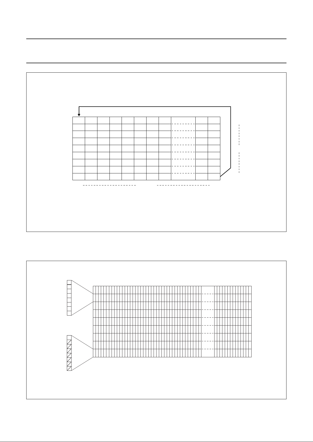
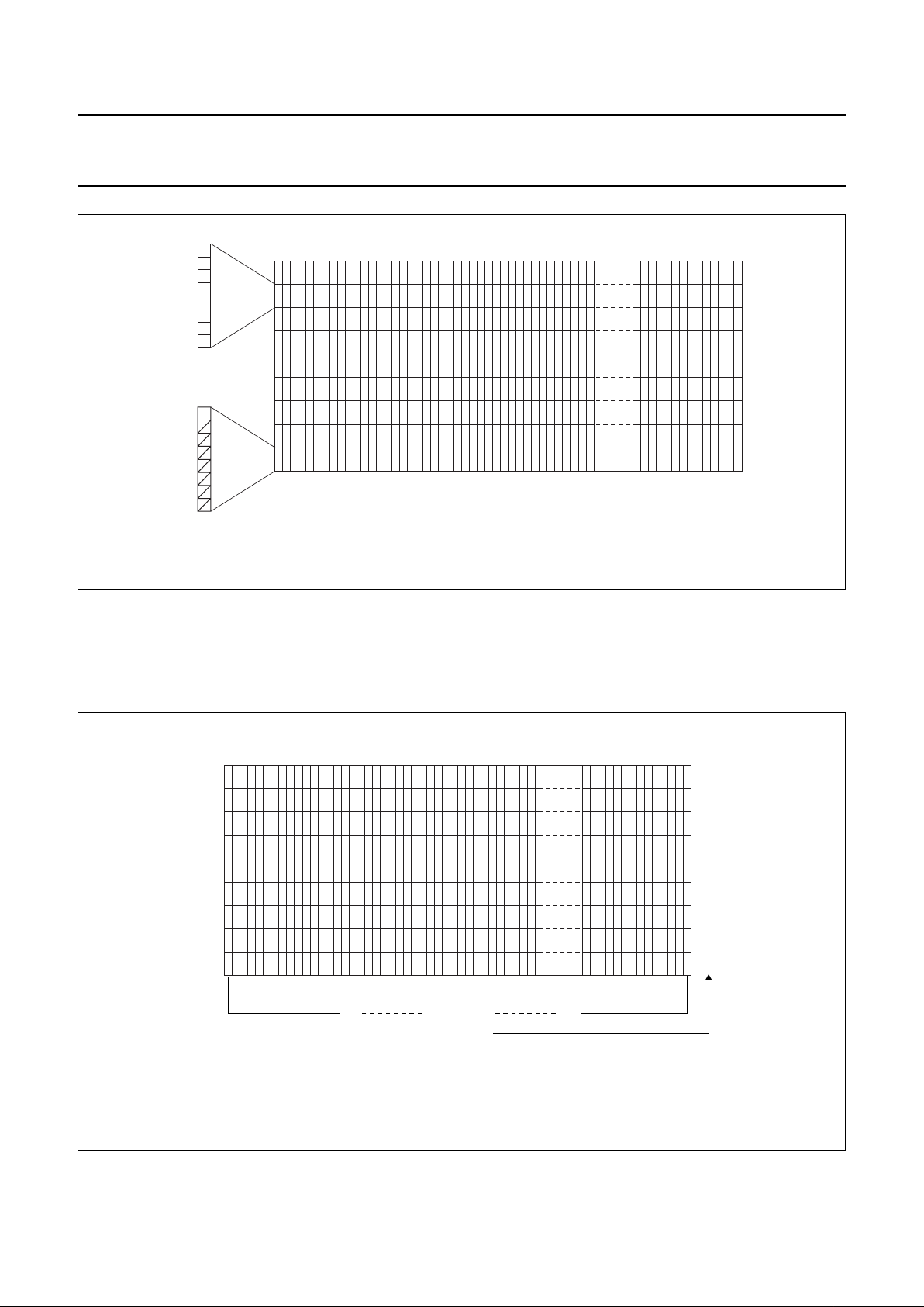
10 ADDRESSING
The Display Data RAM (DDRAM) of the PCF8548 is accessed as indicated in Figs 3, 6, 7, 8 and 9. The DDRAM has a
matrix of 65 × 102 bits. The RAM cells are addressed by the X and Y address pointers. The address ranges are X0 to
X101 (1100101b) and Y0 to Y8(1000b). Addressesoutside ofthese rangesare not allowed. In verticaladdressing mode
(V = 1) the Y address increments after each byte (see Fig.5). After the last Y address (Y = 8), Y wraps around to 0 and
X incrementsto addressthe nextcolumn. Inthe horizontaladdressing mode (V = 0)the X addressincrements aftereach
byte (see Fig.4). After thelast X address(X = 101), X wraps around to 0 andY increments toaddress thenext row. After
the very last address (X = 101 and Y = 8) the address pointers wrap around to address X = 0 andY=0.
10.1 Display data RAM structure
Fig.4 Sequence of writing data bytes into RAM with horizontal addressing (V = 0).
handbook, full pagewidth
MGS396
012
102 103 104
204 205 206
306 307 308
408 409 410
510 511 512
612 613 614
714 715 716
816 817 818
0
8917
0 101X address
Y address
Page 10
1999 Aug 16 10
Philips Semiconductors Product specification
65 × 102 pixels matrix LCD driver PCF8548
The DO bit defines the bit order (MSB on top or MSB on bottom) for writing to the RAM (see Figs 6 and 7).
Fig.5 Sequence of writing data bytes into RAM with vertical addressing (V = 1).
handbook, full pagewidth
MGS397
09
110
2
3
4
5
6
7
8
0
8917
0 101X address
Y address
Fig.6 RAM byte organization, if DO = 0.
handbook, full pagewidth
MGS398
MSB
LSB
MSB
LSB
Page 11
1999 Aug 16 11
Philips Semiconductors Product specification
65 × 102 pixels matrix LCD driver PCF8548
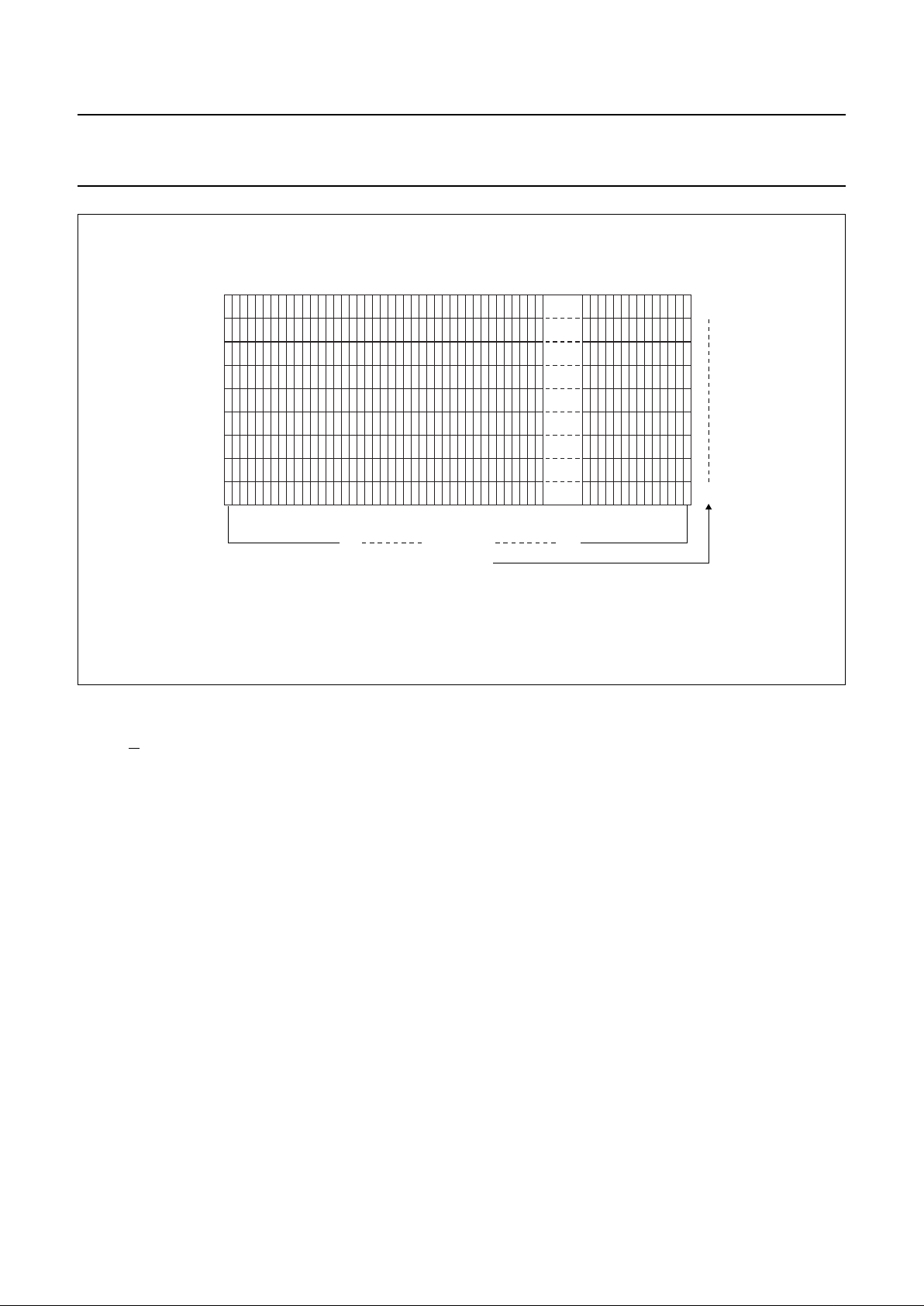
The MX bit allows a horizontal mirroring; when MX = 1, the X address space is mirrored. The address X = 0 is then
located at the right side (column 101) of the display(see Fig.9). When MX = 0 the mirroringis disabled and the address
X = 0 is located at the left side (column 0) of the display (see Fig.8).
Fig.7 RAM byte organization, if DO = 1.
handbook, full pagewidth
MGS399
LSB
MSB
LSB
MSB
Fig.8 RAM format addressing (MX = 0).
handbook, full pagewidth
MGS400
0
8
0 101X address
Y address
Page 12
1999 Aug 16 12
Philips Semiconductors Product specification
65 × 102 pixels matrix LCD driver PCF8548
10.2 RAM access
If the D/C bit is logic 1 the RAM can be written to. The data is written to the RAM during the acknowledge cycle.
Fig.9 RAM format addressing (MX = 1).
handbook, full pagewidth
MBL044
0
8
101 0X address
Y address
Page 13

1999 Aug 16 13
Philips Semiconductors Product specification
65 × 102 pixels matrix LCD driver PCF8548
11 I2C-BUS INTERFACE
11.1 Characteristics of the I
2
C-bus
The I2C-bus is for bidirectional, two-line communication
between different ICs or modules. The two lines are a
Serial Data line(SDA) and a Serial Clockline (SCL). Both
lines must be connected to a positive supply via a pull-up
resistor. Data transfer may be initiated only when the bus
is not busy.
11.1.1 B
IT TRANSFER
One data bit is transferred during each clock pulse.
The data on the SDA line must remain stable during the
HIGH period of the clock pulse because changes in the
data line at this time willbe interpreted as acontrol signal.
Bit transfer is illustrated in Fig.10.
11.1.2 START AND STOP CONDITIONS
Bothdata andclock lines remainHIGH whenthe bus isnot
busy. AHIGH-to-LOW transition of thedata line, while the
clock is HIGH is defined as the START condition (S).
A LOW-to-HIGH transition of the data line while the clock
is HIGH is definedas theSTOP condition (P).The START
and STOP conditions are illustrated in Fig.11.
11.1.3 SYSTEM CONFIGURATION
The system configuration is illustrated in Fig.12.
• Transmitter: the device which sends the data to the bus
• Receiver: the device which receives the data from the
bus
• Master: the device which initiates a transfer, generates
clock signals and terminates a transfer
• Slave: the device addressed by a master
• Multi-Master: more than one master can attempt to
control the bus at the same time without corrupting the
message
• Arbitration: procedure to ensure that, if more than one
master simultaneously tries to control the bus, only one
is allowed to do so and the message is not corrupted
• Synchronization: procedure to synchronize the clock
signals of two or more devices.
11.1.4 A
CKNOWLEDGE
Each byte of eight bits is followed by an acknowledge bit.
Theacknowledge bitisa HIGHsignalput onthebus bythe
transmitter during which time the master generates an
extra acknowledge related clock pulse. A slave receiver
which is addressed must generate an acknowledge after
the reception of each byte. A master receiver must also
generate an acknowledge after the receptionof each byte
that has been clocked out of the slave transmitter.
The device that acknowledges must pull-down the SDA
line during the acknowledge clock pulse, so that the SDA
line is stable LOW during the HIGH period of the
acknowledge related clock pulse (set-up and hold times
must betaken into consideration). A master receiver must
signal an end-of-data to the transmitter by not generating
anacknowledge onthe lastbyte thathas beenclocked out
of the slave. In this event the transmitter must leave the
data line HIGH to enable the master to generate a STOP
condition. Acknowledgement on the I2C-bus is illustrated
in Fig.13.
Fig.10 Bit transfer.
handbook, full pagewidth
MBC621
data line
stable;
data valid
change
of data
allowed
SDA
SCL
Page 14

1999 Aug 16 14
Philips Semiconductors Product specification
65 × 102 pixels matrix LCD driver PCF8548
Fig.11 Definition of START and STOP conditions.
handbook, full pagewidth
MBC622
SDA
SCL
P
STOP condition
SDA
SCL
S
START condition
Fig.12 System configuration.
MGA807
SDA
SCL
MASTER
TRANSMITTER/
RECEIVER
MASTER
TRANSMITTER
SLAVE
TRANSMITTER/
RECEIVER
SLAVE
RECEIVER
MASTER
TRANSMITTER/
RECEIVER
Fig.13 Acknowledgement on the I2C-bus.
handbook, full pagewidth
MBC602
S
START
condition
9821
clock pulse for
acknowledgement
not acknowledge
acknowledge
DATA OUTPUT
BY TRANSMITTER
DATA OUTPUT
BY RECEIVER
SCL FROM
MASTER
Page 15

1999 Aug 16 15
Philips Semiconductors Product specification
65 × 102 pixels matrix LCD driver PCF8548
11.2 I2C-bus protocol
The PCF8548 supports command, data write and status
read access.
Before any data is transmitted on the I2C-bus, the device
which should respond is addressed first. Two 7-bit slave
addresses (0111100 and 0111101) are reserved for the
PCF8548. The least significant bit of the slave address is
set by connecting the input SA0 to either logic 0 (V
SS1
)or
logic 1 (V
DD1
).
The I2C-bus protocol is illustrated in Fig.14.
The sequenceis initiated with a STARTcondition (S) from
the I2C-bus master whichis followedby theslave address.
All slaveswith the correspondingaddress acknowledge in
parallel, all theothers willignore theI2C-bus transfer. After
acknowledgement, one or more command words follow
which define the status of the addressed slaves.
A command wordconsists ofa control byte, which defines
Co and D/C, plus a data byte (see Fig.14 and Table 1).
The last control byte is tagged with a cleared most
significant bit (i.e. the continuation bit Co). After a control
byte with a cleared Co bit, only data bytes will follow. The
state of the D/C bit defines whether the data byte is
interpreted as a command or as RAM data.
The control and data bytes are also acknowledged by all
addressed slaves on the bus.
Afterthe lastcontrolbyte, depending ontheD/
Cbit setting,
either a series of display data bytes or command data
bytes may follow. If the D/C bit is set to logic 1, these
display bytesare storedin the display RAM atthe address
specified by the data pointer. The data pointer is
automatically updated and the data is directed to the
intended PCF8548 device.If the D/C bit of the last control
byte is set to logic 0, these command bytes will be
decoded and the setting of the device will be changed
according to the received commands. The
acknowledgement after each byte is made only by the
addressed slave. At the end of the transmission the
I2C-bus master issues a STOP condition (P).
If the R/W bit is set to logic 1 the chip will output data
immediately after the slave address if the D/C bit, which
was sent during thelast writeaccess, isset tologic 0. If no
acknowledge is generated by the master after a byte, the
driver stops transferring data to the master.
Fig.14 I2C-bus protocol.
handbook, full pagewidth
MGS401
R/
W
S
A
0
S011110
S
A
0
0A
acknowledgement
from PCF8548
acknowledgement
from PCF8548
acknowledgement
from PCF8548
acknowledgement
from PCF8548
acknowledgement
from PCF8548
1
control byte
A data byte data byte
n ≥ 0 bytes
1 byteslave address
Write mode
command word MSB . . . . . . . . . . . LSB
2n ≥ 0 bytes
A
CoCo
0A AP
DC
control byte
control byte
DC
S011110
S
A
0
1A
acknowledgement
from PCF8548
acknowledgement
from master
PCF8548
slave address
status bytes
A
slave address
Read mode
Co
AP
000000
DC
1101 10
Page 16

1999 Aug 16 16
Philips Semiconductors Product specification
65 × 102 pixels matrix LCD driver PCF8548
12 INSTRUCTIONS
The instruction format is divided into two modes:
1. If D/C is set LOW, commands can be sent to the chip.
2. If D/C is set HIGH, the DDRAM will be accessed.
Every instruction can be sent in any order to the PCF8548.
Table 1 Instruction set
INSTRUCTION D/CR/W
COMMAND BYTE
DESCRIPTION
B7 B6 B5 B4 B3 B2 B1 B0
H=0or1
NOP 0000000000no operation
Reserved 0000000001do not use
Function set 00001MXMYPDVHPower-down control; entry
mode; extended instruction
set control (H)
Read status byte 0 1 PD TRS BRS D E MX MY DO read status byte
Write data 1 0 D
7
D
6
D
5
D
4
D
3
D
2
D
1
D0writes data to RAM
H=0
Reserved 000000001Xdo not use
Set V
LCD
range 000000010PRSV
LCD
programming range
select
Display control 0000001D0Esets display configuration
Set HV-gen
stages
00000100S1S0#of HV-gen voltage
multiplication
Set Yaddress of
RAM
000100Y
3
Y
2
Y
1
Y
0
sets Yaddress of RAM:
0 ≤ Y ≤ 8
Set X address of
RAM
001X
6
X
5
X
4
X
3
X
2
X
1
X
0
sets X address of RAM:
0 ≤ X ≤ 101
H=1
Reserved 000000001Xdo not use
Temperature
control
00000001TC
1TC0
set temperature coefficient
(TCx)
Display
configuration
0000001DOTRSBRStop/bottom row mode set data
order
Bias system 0000010BS
2BS1
BS0set bias system (BSx)
Reserved 0001XXXXXXdo not use (reserved for test)
Set V
OP
001V
OP6VOP5VOP4VOP3VOP2VOP1VOP0
write VOP to register
Page 17

1999 Aug 16 17
Philips Semiconductors Product specification
65 × 102 pixels matrix LCD driver PCF8548
Table 2 Explanations of symbols in Table 1
12.1 External reset (
RES)
After power-on a reset pulse must be applied immediately to the chip, as it is in an undefined state. A reset of the chip
can be achieved using the external reset pad. After the reset the LCD driver is set to the following states:
• Power-down mode (PD = 1)
• All LCD outputs at VSS (display off)
• Horizontal addressing (V = 0)
• Normal instruction set (H = 0)
• Normal display (MX = MY = TRS = BRS = 0)
• Display blank (E = D = 0)
• Address counter X[6:0] = 0 and Y[3:0] = 0
• Temperature coefficient (TC[1:0] = 0)
• Bias system (BS[2:0] = 0)
• V
LCD
is equal to 0, the HV generator is switched off (Vop[6:0] = 0 and PRS = 0)
• After power-on (RAM data is undefined), the reset signal does not change the content of the RAM.
BIT 0 1 RESET STATE
PD chip is active chip is in Power-down mode 1
V horizontal addressing vertical addressing 0
H use basic instruction set use extended instruction set 0
MX normal X addressing X address is mirrored 0
MY display is not vertically mirrored display is vertically mirrored 0
TRS top rows are not mirrored top rows are mirrored 0
BRS bottom rows are not mirrored bottom rows are mirrored 0
DO MSB is on top LSB is on top 0
PRS V
LCD
programming range LOW V
LCD
programming range HIGH 0
D and E 00 display blank D = 0
E=0
10 normal mode
01 all display segments on
11 inverse video mode
TC[1:0] 00 V
LCD
temperature coefficient 0 TC[1:0] = 00
01 V
LCD
temperature coefficient 1
10 V
LCD
temperature coefficient 2
11 V
LCD
temperature coefficient 3
S[1:0] 00 2 × voltage multiplier S[1:0] = 00
01 3 × voltage multiplier
10 4 × voltage multiplier
11 5 × voltage multiplier
BS[2:0] bias system BS[2:0] = 000
Vop[6:0] V
LCD
programming Vop[6:0] = 0000000
Page 18

1999 Aug 16 18
Philips Semiconductors Product specification
65 × 102 pixels matrix LCD driver PCF8548
12.2 Function set
12.2.1 POWER-DOWN (PD)
• All LCD outputs at VSS (display off)
• Bias generator and V
LCD
generator off
• Oscillator off (external clock possible)
• V
LCD
can be disconnected
• RAM contents not cleared (RAM data can be written)
• V
LCD
output is discharged to VSS.
12.2.2 V
When V = 0, the horizontal addressing is selected.
The data is written to the RAM as shown in Fig.4. When
V = 1, the vertical addressing is selected. The data is
written to the RAM as shown in Fig.5.
12.2.3 H
When H = 0 the commands ‘display control’, ‘set HV-gen
stages’, ‘set Y address’ and ‘set X address’ can be
performed. When H = 1 the other commands can be
executed. The commands ‘write data’ and ‘function set’
can be executed in both cases.
12.2.4 MX
When MX = 0, the display RAM is written from left to right
(X = 0 is on the left side of the display, X = 100 is on the
right sideof thedisplay). When MX = 1the display RAM is
written from right to left (X = 0 is on the right side of the
display, X = 100 is on the left side of the display).
Thus,if ahorizontally mirroring ofthe displayisdesired the
RAM must first be rewritten.
12.2.5 MY
When MY = 1, the display is mirrored vertically.
A change of thisbit hasan immediateeffect onthe display.
12.3 Display control
12.3.1 D AND E
The bits D and E select the display mode (see Table 2).
12.4 Display configuration
12.4.1 TRS
Bit TRS enables the top row pad blocks to be mirrored.
This is used to enable flexibility in the wiring of the row
lines from the PCF8548 to theLCD cell (e.g. COGor TCP
wiring). When TRS = 0 rows 19 to 32 and rows 51 to 64
are organizedas illustrated in Fig.22. WhenTRS = 1 rows
19 to 32 and rows 51 to 64 are mirrored and organized as
illustrated in Fig.23.
12.4.2 BRS
BitBRS enablesthe bottomrow pad blocksto bemirrored.
This is used to enable flexibility in the wiring of the row
lines from the PCF8548 to theLCD cell (e.g. COGor TCP
wiring). When BRS = 0rows 0 to 18and rows33 to 50 are
organized as illustrated in Fig.22. When BRS = 1 rows
0 to 18 and rows 33 to 50 are mirrored and organized as
illustrated in Fig.23.
12.5 Set Yaddress of RAM
Y[3 : 0] defines the Y address vector address of the RAM.
Table 3 X and Y address ranges
Note
1. In bank 8 only the MSB is accessed.
Y
3
Y
2
Y
1
Y
0
CONTENT ALLOWED X RANGE
0 0 0 0 bank 0 (display RAM) 0 to 101
0 0 0 1 bank 1 (display RAM) 0 to 101
0 0 1 0 bank 2 (display RAM) 0 to 101
0 0 1 1 bank 3 (display RAM) 0 to 101
0 1 0 0 bank 4 (display RAM) 0 to 101
0 1 0 1 bank 5 (display RAM) 0 to 101
0 1 1 0 bank 6 (display RAM) 0 to 101
0 1 1 1 bank 7 (display RAM) 0 to 101
1 0 0 0 bank 8 (display RAM); note 1 0 to 101
Page 19

1999 Aug 16 19
Philips Semiconductors Product specification
65 × 102 pixels matrix LCD driver PCF8548
12.6 Set X address of RAM
The X address points to the columns. The range of X is
0 to 101 (65H).
12.7 Set HV generator stages
12.7.1 S[1:0]
The PCF8548 incorporates a software configurable
voltage multiplier. After reset the voltage multiplier is set to
2 × V
DD2
. Other voltage multiplier factors are set via the
command ‘set HV-gen stages’ (see Tables 1 and 2).
12.8 Temperature control
Due to the temperature dependency of the liquid crystals
viscosity, the LCD controlling voltage V
LCD
must be
increased with lower temperature to maintain optimum
contrast.
There are 4 different temperature coefficients available in
the PCF8548 (see Fig.15). The coefficients are selected
bythe twobits TC[1:0].Table 6 shows thetypical valuesof
the differenttemperature coefficients.The coefficients are
proportional to the programmed V
LCD
.
12.9 Bias system
The Bias voltage levels are set in the ratio
of R − R − nR − R − R giving a bias system.
The resulting bias levels are shown in Table 5.
Different multiplex rates require different factors n (see
Table 4); this is programmed by BS[2 : 0]. For Mux1:65
the optimum bias value n is given by:
resulting in
1
⁄9bias.
1
n4+
------------ -
nm3– 65 3– 5.06 5== ==
Fig.15 Temperature coefficients.
handbook, halfpage
MGS402
T
V
LCD
T
cut
Page 20

1999 Aug 16 20
Philips Semiconductors Product specification
65 × 102 pixels matrix LCD driver PCF8548
Table 4 Programming the required bias system
BS[2] BS[1] BS[0] n RECOMMENDED MUX RATE
0007 1:100
0016 1:81
0105 1:64
0114 1:49
1003 1:36
1012 1:24
1101 1:16
1110 1:9
Table 5 LCD bias voltage
12.10 Set VOP value
The voltage at reference temperature can be calculated
as: [V
LCD
(T = T
cut
)]
(1)
The operating voltage V
LCD
can be set by software.
The generated voltage is dependent on the temperature,
programmed Temperature Coefficient (TC) and the
programmed voltage at reference temperature (T
cut
).
(2)
SYMBOL BIAS VOLTAGES
BIAS VOLTAGES
FOR
1
⁄9BIAS
V1 V
LCD
V
LCD
V2 (n + 3)/(n + 4)
8
⁄9× V
LCD
V3 (n + 2)/(n + 4)
7
⁄9× V
LCD
V4 2/(n + 4)
2
⁄9× V
LCD
V5 1/(n + 4)
1
⁄9× V
LCD
V6 V
SS
V
SS
V
LCD
Tcut()
aVOPb×+()=
V
LCD
aVOPb×+()1TT
cut
–()TC×+[]×=
The parameters are explained in Fig.16 and Table 6.
The maximumvoltage thatcan be generatedis dependent
on the V
DD2
voltage and the display load current.
Two overlapping V
LCD
ranges are selectable via the
command ‘HV-gencontrol’. For the LOW (PRS = 0)range
a=a1and forthe HIGH(PRS = 1) range a = a2with steps
equal to b in both ranges. It should be noted that the
chargepump isturned offif VOP[6;0]and bitPRS areall set
to zero. For Mux 1 : 65 the optimum operation voltage of
the liquid can be calculated as follows:
where V
th
is the threshold voltage of the liquid crystal
material used.
V
LCD
165+
21
1
65
----------
–
×
---------------------------------------
V
th
6.85 Vth×=×=
Table 6 Typical values for parameters for the HV-generator programming
SYMBOL BITS VALUE UNIT
a
1
2.94 (PRS = 0) V
a
2
6.75 (PRS = 1) V
b 0.03 V
T
cut
27 °C
Page 21

1999 Aug 16 21
Philips Semiconductors Product specification
65 × 102 pixels matrix LCD driver PCF8548
As theprogramming range for the internally generated V
LCD
allows valuesabove the maximumallowed V
LCD
(9.0 V) the
customer must ensure while setting the VOPregister and selecting the temperature coefficient, under all conditions and
including all tolerances V
LCD
remains below 9.0 V.
handbook, full pagewidth
MGS658
0H 01H 02H
a1+b
a
2
a
1
V
LCD
b
03H 04H 05H 06H
. . . 5FH 6FH 7FH 00H 01H 02H 03H 04H 05H 06H . . . 5FH 6FH 7FH
LOW (PRS = 0
)
HIGH (PRS = 1
)
charge pump off
Fig.16 VOP programming of PCF8548.
VOP[6:0] (programmed); 00H to 7FH, programme range LOW and HIGH.
Page 22

1999 Aug 16 22
Philips Semiconductors Product specification
65 × 102 pixels matrix LCD driver PCF8548
13 LIMITING VALUES
Limiting values given are in accordance with the Absolute Maximum Rating System (IEC 134); parameters are valid
over operating temperature range unless otherwise specified; all voltages referenced to VSS= 0 V. Stress above one or
more of the limiting valuesmay cause permanent damage to the device. These are stress ratings only and operation of
the deviceat these or at any other conditions abovethose given in the characteristics sections of the specification is not
implied. Exposure to limiting values for extended periods may affect device reliability.
14 HANDLING
Inputs and outputs are protected against electrostatic discharge in normal handling. However, to be totally safe, it is
desirable to take normal precautions appropriate to handling MOS devices (see “Handling MOS Devices”).
15 DC CHARACTERISTICS
V
DD1
= 1.9 to 5.5 V; V
DD2
and V
DD3
= 2.4 to 4.5 V; V
SS1
and V
SS2
=0V; V
LCD
= 4.5 to 9.0 V; T
amb
= −40 to +85 °C;
unless otherwise specified.
SYMBOL PARAMETER MIN. MAX. UNIT
V
DD1
supply voltage −0.5 +6.5 V
V
DD2,VDD3
supply voltage for internal voltage generator −0.5 +4.5 V
V
LCD
supply voltage for the LCD −0.5 +9.0 V
I
SS
supply current −50 +50 mA
V
i(n)
all input voltages −0.5 VDD+ 0.5 V
I
I
DC input current −10 +10 mA
I
O
DC output current −10 +10 mA
P
pack
power dissipation per package − 300 mW
P/out power dissipation per output − 30 mW
SYMBOL PARAMETER CONDITIONS MIN. TYP. MAX. UNIT
V
DD1
supply voltage 1.9 − 5.5 V
T
amb
= −25 to +85 °C 1.8 − 5.5 V
V
DD2,VDD3
supply voltage for
internal voltage
generator
LCD voltage internally
generated (voltage generator
enabled)
2.4 − 4.5 V
V
LCDIN
LCD input supply
voltage
LCD voltage externally
supplied (voltage generator
disabled)
4.5 − 9.0 V
V
LCDOUT
LCD output supply
voltage
LCD voltage internally
generated (voltage generator
enabled); note 1
4.5 − 9.0 V
I
DD1
supply current V
DD1
= 2.8 V; V
LCD
= 7.6 V;
f
sclk
= 0; T
amb
=25°C;
notes 2 and 3
− 20 −µA
I
DD2,IDD3
supply current for
internal voltage
generator
with external V
LCD
− 0.5 −µA
with internal V
LCD
generation;
V
DD1
= 2.8 V; V
LCD
= 7.6 V;
f
sclk
= 0; T
amb
=25°C; no
displayload; 4 × charge pump;
notes 2 and 3
− 180 −µA
Page 23

1999 Aug 16 23
Philips Semiconductors Product specification
65 × 102 pixels matrix LCD driver PCF8548
Notes
1. The maximum possible V
LCD
voltage thatcan begenerated is dependenton voltage, temperature and (display)load.
2. Internal clock.
3. When f
sclk
= 0 there is no I2C-bus clock.
4. Power-down mode. During power-down all static currents are switched off.
5. If external V
LCD
, the display load current is not transmitted to IDD.
6. Tolerance depends on the temperature; (typically zero at T
amb
=27°C), maximum tolerance values are measured
at the temperature range limit.
7. For TC0 to TC3.
I
DD(tot)
total supply current with internal V
LCD
generation;
V
DD1
= 2.8 V; V
LCD
= 7.6 V;
f
sclk
= 0; T
amb
=25°C; no
displayload; 4 × charge pump;
notes 2 and 3
− 200 350 µA
(Power-down mode) with
internal or external V
LCD
generation; note 4
− 1.5 10 µA
I
LCDIN
supply current from
external V
LCD
V
DD1
= 2.8 V; V
LCD
= 7.6 V;
f
sclk
= 0; T
amb
=25°C; no
display load; notes 2, 3 and 5
− 30 −µA
Logic
V
IL
LOW-level input voltage V
SS1
− 0.3V
DD1
V
V
IH
HIGH-levelinput voltage 0.7V
DD1
− V
DD1
V
I
L
leakage current Vi=V
DD1
or V
SS1
−1 − +1 µA
Column and row outputs
R
row
row output resistance
R0 to R64
V
DD1
to V
DD3
= 5.0 V;
V
LCD
= 7.6 V; IL=10µA;
outputs tested one at a time
− 12 20 kΩ
R
col
column output
resistance C0 to C101
V
LCD
= 7.6 V − 12 20 kΩ
V
bias(col)
column bias tolerance
C0 to C101
−100 0 +100 mV
V
bias(row)
row bias tolerance
R0 to R64
−100 0 +100 mV
LCD supply voltage generator
V
LCD
V
LCD
tolerance
internally generated
V
DD1
= 2.8 V; V
LCD
= 7.6 V;
f
sclk
= 0; T
amb
=25°C;
no display load;
notes 2, 3 6 and 7
−300 0 +300 mV
TC temperature coefficient 00 −−0.0 × 10
−3
− 1/°C
01 −−0.76 × 10
−3
− 1/°C
10 −−1.05 × 10
−3
− 1/°C
11 −−2.10 × 10
−3
− 1/°C
SYMBOL PARAMETER CONDITIONS MIN. TYP. MAX. UNIT
Page 24

1999 Aug 16 24
Philips Semiconductors Product specification
65 × 102 pixels matrix LCD driver PCF8548
16 AC CHARACTERISTICS
V
DD1
= 1.9 to 5.5 V; V
DD2
and V
DD3
= 2.4 to 4.5 V; V
SS1
and V
SS2
=0V; V
LCD
= 4.5 to 9 V; T
amb
= −40 to +85 °C;
unless otherwise specified.
Notes
1.
2.
RES may be LOW before V
DD1
goes HIGH.
3. If t
W(RES)
is longer than 3 ns (typical) a reset may be generated.
4. All timing values are valid within the operating supply voltage and ambient temperature ranges and are referenced
to VIL and VIH with an input voltage swing of VSS to VDD.
5. The rise and fall times specified here refer to the driver device (i.e. not PCF8548) and are part of the general fast
I2C-bus specification. When PCF8548 asserts an acknowledge on SDA, the minimum fall time is 10 ns.
Cb= capacitive load per bus line.
6. The device inputs SDA and SCL are filtered and will reject spikes on the bus lines of width <t
SW(max)
.
SYMBOL PARAMETER CONDITIONS MIN. TYP. MAX. UNIT
f
OSC
oscillator frequency V
DD1
= 2.8 V;
T
amb
= −20 to +70 °C
20 38 70 kHz
f
clk(ext)
external clock frequency 20 38 100 kHz
f
frame
frame frequency f
OSC
or f
clk(ext)
= 38 kHz;
note 1
− 73 − Hz
t
VHRL
V
DD1
to RES LOW see Fig.17 and note 2 0 − 1 µs
t
W(RES)
RES LOW pulse width see Fig.17 and note 3 100 −−ns
I
2
C-bus timing characteristics; see note 4
f
SCLK
SCL clock frequency 0 − 400 kHz
t
SCLL
SCL clock LOW period 1.3 −−µs
t
SCLH
SCL clock HIGH period 0.6 −−µs
t
SU;DAT
data set-up time 100 −−ns
t
HD;DAT
data hold time 0 − 0.9 µs
t
r
SCL and SDA rise time note 5 20 + 0.1Cb− 300 ns
t
f
SCL and SDA fall time note5 20 + 0.1Cb− 300 ns
t
f(SDA)(ro)
SDA fall time for read out V
DD1
= <3.6 V 20 + 0.1Cb− 1000 ns
C
b
capacitive load represented by each
bus line
−−400 pF
t
SU;STA
set-up time for a repeated START
condition
0.6 −−µs
t
HD;STA
START condition hold time 0.6 −−µs
t
SU;STO
set-up time for STOP condition 0.6 −−µs
t
SW
tolerable spike width on bus note 6 −−50 ns
t
BUF
bus free time between a STOP and
START condition
1.3 −−µs
f
frame
f
clk ext()
520
------------------
=
Page 25

1999 Aug 16 25
Philips Semiconductors Product specification
65 × 102 pixels matrix LCD driver PCF8548
17 RESET
Fig.17 Reset timing.
handbook, full pagewidth
MGS404
t
VHRL
t
W(RES)
t
W(RES)
t
W(RES)
t
W(RES)
V
DD
RES
V
DD
RES
Page 26

1999 Aug 16 26
Philips Semiconductors Product specification
65 × 102 pixels matrix LCD driver PCF8548
18 APPLICATION INFORMATION
Table 7 Programming example for PCF8548
STEP
BITS
DISPLAY OPERATION
B7 B6 B5 B4 B3 B2 B1 B0
1I
2
C-bus start
2 01111000 slave address for write
3 00000000 control byte with cleared Co
bit and D/C set to logic 0
4 00100001 function set; PD = 0; V = 0;
select extended instruction
set (H = 1 mode)
5 00010010 setbias system 2; this is the
recommended bias system
for a multiplex rate1:65
6 11101010 set V
OP
; VOP is set to a
+106 × b [V]; it should be
noted that the required
voltage is dependent on the
liquid
7 00100000 function set; PD = 0; V = 0;
select normal instruction set
(H = 0 mode)
8 00001100 display control; set normal
mode (D = 1; E = 0)
9I
2
C-bus start restart; to write into the
display RAM the D/C must
be set to logic 1; therefore a
control byte is needed
10 01111000 slave address for write
11 01000000 control byte with cleared Co
bit and D/
C set to logic 1
12 11111000 data write; Yand X are
initialized to 0 by default, so
they are not set here
13 10100000 data write
MGS405
MGS406
Page 27

1999 Aug 16 27
Philips Semiconductors Product specification
65 × 102 pixels matrix LCD driver PCF8548
14 11100000 data write
15 00000000 data write
16 11111000 data write
17 00100000 data write
18 11111000 data write
19 I
2
C-bus start restart
20 01111000 slave address for write
21 10000000 control byte with set Co bit
and D/C set to logic 0
22 00001101 display control; set inverse
video mode (D = 1; E = 1)
23 10000000 control byte with set Co bit
and D/
C set to logic 0
24 10000000 set X address of RAM; set
address to ‘0000000’
STEP
BITS
DISPLAY OPERATION
B7 B6 B5 B4 B3 B2 B1 B0
MGS407
MGS408
MGS409
MGS410
MGS411
MGS412
MGS413
Page 28

1999 Aug 16 28
Philips Semiconductors Product specification
65 × 102 pixels matrix LCD driver PCF8548
25 11000000 control byte with set Co bit
and D/C set to logic 1
26 00000000 data write
27 00000000 control byte with cleared Co
bit and D/
C set to logic 0
28 10000000 set X address of RAM; set
address to ‘0000000’
29 I
2
C-bus start restart
30 01111000 slave address for write
31 11000000 control byte with set Co bit
and D/
C set to logic 1
32 11111000 write data
33 10000000 control byte with set Co bit
and D/
C set to logic 0
STEP
BITS
DISPLAY OPERATION
B7 B6 B5 B4 B3 B2 B1 B0
MGS414
MGS415
MGS416
Fig.18 Connecting the I2C-bus interface.
handbook, halfpage
SCLSCL
SDAIN
SDAOUT
SDA
V
DD1
V
DD1
PCF8548
MICRO-
CONTROLLER
MGS417
Page 29

1999 Aug 16 29
Philips Semiconductors Product specification
65 × 102 pixels matrix LCD driver PCF8548
Fig.19 Internal charge pump is used and a single supply voltage.
The number of I/Os depends on the application.
handbook, full pagewidth
MGS418
≥3
DISPLAY 102 × 65
V
DD2,3VDD1
V
DD
I/O
V
SS
C
VLCD
C
VDD
V
SS1VSS2VLCDSENSE
V
LCDOUTVLCDIN
PCF8548
10232 33
Fig.20 Internal charge pump is used and two separate supply voltages.
The number of I/Os depends on the application.
handbook, full pagewidth
MGS419
≥3
DISPLAY 102 × 65
V
DD2,3VDD1
V
DD2
V
DD1
I/O
V
SS
C
VLCD
C
VDD2
V
SS1VSS2VLCDSENSE
V
LCDOUTVLCDIN
C
VDD1
PCF8548
10232 33
Page 30

1999 Aug 16 30
Philips Semiconductors Product specification
65 × 102 pixels matrix LCD driver PCF8548
Fig.21 External high voltage generation is used.
The number of I/Os depends on the application.
handbook, full pagewidth
MGS420
≥3
DISPLAY 102 × 65
V
DD2,3VDD1
V
DD
I/O
V
SS
V
LCD
C
VDD
V
SS1VSS2VLCDSENSE
V
LCDOUTVLCDIN
PCF8548
10232 33
The pinning of the PCF8548 is optimized for single plane wiring e.g. for chip-on-glass display modules, or for TCP.
Displaysize: 65 × 102 pixels.The requiredminimum valuefor theexternal capacitorsin anapplication with the PCF8548
are: C
VDD
, C
VDD1
, C
VDD2
and C
VLCD
= 1.0 µF (min.). Higher capacitor values are recommended for ripple reduction.
To reduce the sensitivity of the reset to ESD/EMC disturbances for a COG application, it is strongly recommended to
implement on the glass (ITO) a series input resistance in the reset line (The recommended minimum value is 8 kΩ).
19 CHIP INFORMATION
The PCF8548 is manufactured in n-well CMOS technology. The substrate is at VSS potential.
20 PAD INFORMATION
PAD VALUE UNIT
Minimum bump pitch 70 µm
Pad size, alumin 62 × 100 µm
Bumps 50 (±6) × 90 (±6) × 17.5 (±5) µm
Wafer thickness without bumps U/2 = 381; U/9 = 525 µm
Page 31

1999 Aug 16 31
Philips Semiconductors Product specification
65 × 102 pixels matrix LCD driver PCF8548
Table 8 Bonding pad location
All x and y coordinates are referenced to the centre of the
chip (dimension in µm; see Fig.22).
SYMBOL PAD x y
RES 1 +1160 +899.4
SDAOUT 2 +840 +899.4
SDAIN 3 +600 +899.4
SDAIN 4 +520 +899.4
SCL 5 +200 +899.4
SCL 6 +120 +899.4
T2 7 −200 +899.4
SA0 8 −410 +899.4
T7 9 −620 +899.4
T6 10 −830 +899.4
T5 11 −1040 +899.4
T4 12 −1250 +899.4
T3 13 −1460 +899.4
T1 14 −1670 +899.4
V
SS1
15 −1750 +899.4
V
SS1
16 −1830 +899.4
V
SS1
17 −1910 +899.4
V
SS1
18 −1990 +899.4
V
SS1
19 −2070 +899.4
V
SS1
20 −2150 +899.4
V
SS2
21 −2310 +899.4
V
SS2
22 −2390 +899.4
V
SS2
23 −2470 +899.4
V
SS2
24 −2550 +899.4
V
SS2
25 −2630 +899.4
V
SS2
26 −2710 +899.4
dummy pad 27 −2790 +899.4
V
LCDOUT
28 −2950 +899.4
V
LCDOUT
29 −3030 +899.4
V
LCDOUT
30 −3110 +899.4
V
LCDOUT
31 −3190 +899.4
V
LCDOUT
32 −3270 +899.4
V
LCDOUT
33 −3350 +899.4
V
LCDSENSE
34 −3430 +899.4
V
LCDIN
35 −3510 +899.4
V
LCDIN
36 −3590 +899.4
V
LCDIN
37 −3670 +899.4
V
LCDIN
38 −3750 +899.4
V
LCDIN
39 −3830 +899.4
V
LCDIN
40 −3910 +899.4
R32 41 −4235 +899.4
R31 42 −4305 +899.4
R30 43 −4375 +899.4
R29 44 −4445 +899.4
R28 45 −4515 +899.4
R27 46 −4585 +899.4
R26 47 −4655 +899.4
R25 48 −4725 +899.4
R24 49 −4795 +899.4
R23 50 −4865 +899.4
R22 51 −4935 +899.4
R21 52 −5005 +899.4
R20 53 −5075 +899.4
R19 54 −5145 +899.4
dummy pad 55 −5355 +899.4
dummy pad 56 −5320 −899.4
R0 57 −5040 −899.4
R1 58 −4970 −899.4
R2 59 −4900 −899.4
R3 60 −4830 −899.4
R4 61 −4760 −899.4
R5 62 −4690 −899.4
R6 63 −4620 −899.4
R7 64 −4550 −899.4
R8 65 −4480 −899.4
R9 66 −4410 −899.4
R10 67 −4340 −899.4
R11 68 −4270 −899.4
R12 69 −4200 −899.4
R13 70 −4130 −899.4
R14 71 −4060 −899.4
R15 72 −3990 −899.4
R16 73 −3920 −899.4
R17 74 −3850 −899.4
R18 75 −3780 −899.4
C0 76 −3570 −899.4
C1 77 −3500 −899.4
C2 78 −3430 −899.4
C3 79 −3360 −899.4
C4 80 −3290 −899.4
SYMBOL PAD x y
Page 32

1999 Aug 16 32
Philips Semiconductors Product specification
65 × 102 pixels matrix LCD driver PCF8548
C5 81 −3220 −899.4
C6 82 −3150 −899.4
C7 83 −3080 −899.4
C8 84 −3010 −899.4
C9 85 −2940 −899.4
C10 86 −2870 −899.4
C11 87 −2800 −899.4
C12 88 −2730 −899.4
C13 89 −2660 −899.4
C14 90 −2590 −899.4
C15 91 −2520 −899.4
C16 92 −2450 −899.4
C17 93 −2380 −899.4
C18 94 −2310 −899.4
C19 95 −2240 −899.4
C20 96 −2170 −899.4
C21 97 −2100 −899.4
C22 98 −2030 −899.4
C23 99 −1960 −899.4
C24 100 −1890 −899.4
C25 101 −1750 −899.4
C26 102 −1680 −899.4
C27 103 −1610 −899.4
C28 104 −1540 −899.4
C29 105 −1470 −899.4
C30 106 −1400 −899.4
C31 107 −1330 −899.4
C32 108 −1260 −899.4
C33 109 −1190 −899.4
C34 110 −1120 −899.4
C35 111 −1050 −899.4
C36 112 −980 −899.4
C37 113 −910 −899.4
C38 114 −840 −899.4
C39 115 −770 −899.4
C40 116 −700 −899.4
C41 117 −630 −899.4
C42 118 −560 −899.4
C43 119 −490 −899.4
C44 120 −420 −899.4
C45 121 −350 −899.4
C46 122 −280 −899.4
SYMBOL PAD x y
C47 123 −210 −899.4
C48 124 −140 −899.4
C49 125 −70 −899.4
C50 126 +0 −899.4
C51 127 +140 −899.4
C52 128 +210 −899.4
C53 129 +280 −899.4
C54 130 +350 −899.4
C55 131 +420 −899.4
C56 132 +490 −899.4
C57 133 +560 −899.4
C58 134 +630 −899.4
C59 135 +700 −899.4
C60 136 +770 −899.4
C61 137 +840 −899.4
C62 138 +910 −899.4
C63 139 +980 −899.4
C64 140 +1050 −899.4
C65 141 +1120 −899.4
C66 142 +1190 −899.4
C67 143 +1260 −899.4
C68 144 +1330 −899.4
C69 145 +1400 −899.4
C70 146 +1470 −899.4
C71 147 +1540 −899.4
C72 148 +1610 −899.4
C73 149 +1680 −899.4
C74 150 +1750 −899.4
C75 151 +1820 −899.4
C76 152 +1890 −899.4
C77 153 +2030 −899.4
C78 154 +2100 −899.4
C79 155 +2170 −899.4
C80 156 +2240 −899.4
C81 157 +2310 −899.4
C82 158 +2380 −899.4
C83 159 +2450 −899.4
C84 160 +2520 −899.4
C85 161 +2590 −899.4
C86 162 +2660 −899.4
C87 163 +2730 −899.4
C88 164 +2800 −899.4
SYMBOL PAD x y
Page 33

1999 Aug 16 33
Philips Semiconductors Product specification
65 × 102 pixels matrix LCD driver PCF8548
Table 9 Alignment marks
The alignment marks are circular with a diameter of
100 µm.
C89 165 +2870 −899.4
C90 166 +2940 −899.4
C91 167 +3010 −899.4
C92 168 +3080 −899.4
C93 169 +3150 −899.4
C94 170 +3220 −899.4
C95 171 +3290 −899.4
C96 172 +3360 −899.4
C97 173 +3430 −899.4
C98 174 +3500 −899.4
C99 175 +3570 −899.4
C100 176 +3640 −899.4
C101 177 +3710 −899.4
R50 178 +3850 −899.4
R49 179 +3920 −899.4
R48 180 +3990 −899.4
R47 181 +4060 −899.4
R46 182 +4130 −899.4
R45 183 +4200 −899.4
R44 184 +4270 −899.4
R43 185 +4340 −899.4
R42 186 +4410 −899.4
R41 187 +4480 −899.4
R40 188 +4550 −899.4
R39 189 +4620 −899.4
R38 190 +4690 −899.4
R37 191 +4760 −899.4
R36 192 +4830 −899.4
R35 193 +4900 −899.4
R34 194 +4970 −899.4
R33 195 +5040 −899.4
dummy pad 196 +5320 −899.4
dummy pad 197 +5355 +899.4
R51 198 +5145 +899.4
R52 199 +5075 +899.4
R53 200 +5005 +899.4
R54 201 +4935 +899.4
R55 202 +4865 +899.4
R56 203 +4795 +899.4
R57 204 +4725 +899.4
R58 205 +4655 +899.4
R59 206 +4585 +899.4
SYMBOL PAD x y
R60 207 +4515 +899.4
R61 208 +4445 +899.4
R62 209 +4375 +899.4
R63 210 +4305 +899.4
R64 211 +4235 +899.4
T12 212 +3880 +899.4
T11 213 +3720 +899.4
T10 214 +3560 +899.4
T9 215 +3400 +899.4
OSC 216 +3160 +899.4
T8 217 +2680 +899.4
V
DD1
218 +2600 +899.4
V
DD1
219 +2520 +899.4
V
DD1
220 +2440 +899.4
V
DD1
221 +2360 +899.4
V
DD1
222 +2280 +899.4
V
DD1
223 +2200 +899.4
V
DD3
224 +2120 +899.4
V
DD3
225 +2040 +899.4
V
DD3
226 +1960 +899.4
V
DD2
227 +1880 +899.4
V
DD2
228 +1800 +899.4
V
DD2
229 +1720 +899.4
V
DD2
230 +1640 +899.4
V
DD2
231 +1560 +899.4
V
DD2
232 +1480 +899.4
V
DD2
233 +1400 +899.4
x y MARKS
+5214 −899.4 mark 1
−5214 −899.4 mark 2
+4099 +899.4 mark 3
−4099 +899.4 mark 4
SYMBOL PAD x y
Page 34

1999 Aug 16 34
Philips Semiconductors Product specification
65 × 102 pixels matrix LCD driver PCF8548
This text is here in white to force landscape pages to be rotated correctly when browsing through the pdf in the Acrobat reader.This text is here in
_white to forcelandscape pages to be rotated correctly when browsing through the pdfin the Acrobat reader.This text is here inThis text is here in
white to force landscape pagesto berotated correctly whenbrowsing throughthe pdfin theAcrobat reader. whiteto forcelandscape pagesto be ...
handbook, full pagewidth
MGS421
OSC
dummy
dummy
dummy
dummy
dummy
row 33
row 50
col 101
row 18
row 0
row 19
row 32
row 64
row 51
col 0
alignment mark
alignment mark
alignment mark
alignment mark
pad No.1
T9
T10
T11
T12
T8
V
DD1
V
DD3
V
DD2
V
SS2
V
SS1
V
LCDOUT
V
LCDIN
V
LCDSENSE
RES
SDAOUT
SDAIN
SCL
PC8548-1
T2
SA0
T1T3T4T5T6
T7
x
y
0,0
.....
.
...
...
.....
.
...
.....
.
...
Maximum chip size: 2.12 mm × 10.99 mm.
Fig.22 Bonding pad location.
Page 35

1999 Aug 16 35
Philips Semiconductors Product specification
65 × 102 pixels matrix LCD driver PCF8548
MGS657
handbook, full pagewidth
R64
R63
TRS = 1
COLUMNS
PC8548-1
R52
R51
.
.
.
.
.
R19
R20
R31
R32
.
.
.
.
.
R50
R49
BRS = 1
COLUMNS
PC8548-1
R34
R33
.
.
.
.
.
R0
R1
R17
R18
.
.
.
.
.
C0
C1
MX = 1
PC8548-1
C100
C101
.
.
.
.
.
.
Fig.23 Pad layout for BRS, TRS and MX.
Page 36

1999 Aug 16 36
Philips Semiconductors Product specification
65 × 102 pixels matrix LCD driver PCF8548
21 DEVICE PROTECTION DIAGRAM
Fig.24 Device protection diagram.
handbook, full pagewidth
MGS422
V
DD1
V
SS1
V
SS1
V
DD3
V
SS1
V
SS1
V
SS2
V
SS1
V
SS1
V
LCDIN
V
LCDOUT
V
LCDSENSE
V
SS1
V
SS1
V
DD2
V
SS1
V
SS2
V
SS1
V
DD1
T2
V
SS1
V
LCDIN
T9
T10
T11
T12
V
SS1
V
DD1
T3, T4
V
SS1
V
LCDIN
COL 0-101/ROW 0-64
1 per block
V
SS1
V
SS1
V
DD1
V
SS1
SA0
OSC
RES
T1
T5 to T7
V
SS1
V
SS1
T8
Page 37

1999 Aug 16 37
Philips Semiconductors Product specification
65 × 102 pixels matrix LCD driver PCF8548
22 TRAY INFORMATION
Fig.25 Tray details.
handbook, full pagewidth
MGS423
D
C
A
x
y
F
E
B
The dimensions are given in Table 10.
Table 10 Dimensions
Fig.26 Tray alignment.
The orientation ofthe IC ina pocket isindicated by theposition of
the IC type name on the die surfacewith respect to thechamfer on
the upper leftcorner of thetray. Refer to the bonding pad location
diagramfor the orientating and position of the type name on the die
surface.
handbook, halfpage
MGS424
PC8548-1
DIM. DESCRIPTION VALUE
A pocket pitch, x direction 13.77 mm
B pocket pitch, y direction 4.45 mm
C pocket width, x direction 11.09 mm
D pocket width, y direction 2.3 mm
E tray width, x direction 50.8 mm
F tray width, x direction 50.8 mm
x number of pockets in
x direction
3
y number of pockets in
y direction
10
Page 38

1999 Aug 16 38
Philips Semiconductors Product specification
65 × 102 pixels matrix LCD driver PCF8548
23 DEFINITIONS
24 LIFE SUPPORT APPLICATIONS
These products are not designed for use in life support appliances, devices, or systems where malfunction of these
products can reasonably be expected to result in personal injury. Philips customers using or selling these products for
use in suchapplications do so at their own risk and agree to fully indemnify Philips for any damages resulting from such
improper use or sale.
25 PURCHASE OF PHILIPS I
2
C COMPONENTS
26 BARE DIE DISCLAIMER
All die are tested and are guaranteed to comply with all data sheet limits up to the point of wafer sawing for a period of
ninety (90) days from the date of Philips' delivery. If there are data sheet limits not guaranteed, these will be separately
indicated in the data sheet. There is no post waffle pack testing performed on individual die. Although the most modern
processes are utilized for wafer sawing and die pick and place into waffle pack carriers, Philips Semiconductors has no
control of third party procedures in the handling, packing or assembly of the die. Accordingly, Philips Semiconductors
assumes no liability for device functionality or performance of the die or systems after handling, packing or assembly of
the die. It is the responsibility of the customer to test and qualify their application in which the die is used.
Data sheet status
Objective specification This data sheet contains target or goal specifications for product development.
Preliminary specification This data sheet contains preliminary data; supplementary data may be published later.
Product specification This data sheet contains final product specifications.
Application information
Where application information is given, it is advisory and does not form part of the specification.
Purchase of Philips I
2
C components conveys a license under the Philips’ I2C patent to use the
components inthe I2C systemprovided the systemconforms to theI2C specificationdefined by
Philips. This specification can be ordered using the code 9398 393 40011.
Page 39

1999 Aug 16 39
Philips Semiconductors Product specification
65 × 102 pixels matrix LCD driver PCF8548
NOTES
Page 40

© Philips Electronics N.V.
SCA
All rights are reserved. Reproduction in whole or in part is prohibited without the prior written consent of the copyright owner.
The information presented in this document does notform part of any quotation or contract, isbelieved to be accurate and reliable and may be changed
without notice. No liability will be accepted by the publisher for any consequence of its use. Publication thereof does not convey nor imply any license
under patent- or other industrial or intellectual property rights.
Internet: http://www.semiconductors.philips.com
1999
67
Philips Semiconductors – a w orldwide compan y
For all other countries apply to: Philips Semiconductors,
International Marketing & Sales Communications, Building BE-p, P.O. Box 218,
5600 MD EINDHOVEN, The Netherlands, Fax. +31 40 27 24825
Argentina: see South America
Australia: 3 Figtree Drive, HOMEBUSH, NSW 2140,
Tel. +61 2 9704 8141, Fax. +61 2 9704 8139
Austria: Computerstr. 6, A-1101 WIEN, P.O. Box 213,
Tel. +43 1 60 101 1248, Fax. +43 1 60 101 1210
Belarus: Hotel Minsk Business Center, Bld. 3, r. 1211, Volodarski Str. 6,
220050 MINSK, Tel. +375 172 20 0733, Fax. +375 172 20 0773
Belgium: see The Netherlands
Brazil: see South America
Bulgaria: Philips Bulgaria Ltd., Energoproject, 15th floor,
51 James Bourchier Blvd., 1407 SOFIA,
Tel. +359 2 68 9211, Fax. +359 2 68 9102
Canada: PHILIPS SEMICONDUCTORS/COMPONENTS,
Tel. +1 800 234 7381, Fax. +1 800 943 0087
China/Hong Kong: 501 Hong Kong Industrial Technology Centre,
72 Tat Chee Avenue, Kowloon Tong, HONG KONG,
Tel. +852 2319 7888, Fax. +852 2319 7700
Colombia: see South America
Czech Republic: see Austria
Denmark: Sydhavnsgade 23, 1780 COPENHAGEN V,
Tel. +45 33 29 3333, Fax. +45 33 29 3905
Finland: Sinikalliontie 3, FIN-02630 ESPOO,
Tel. +358 9 615 800, Fax. +358 9 6158 0920
France: 51 Rue Carnot, BP317, 92156 SURESNES Cedex,
Tel. +33 1 4099 6161, Fax. +33 1 4099 6427
Germany: Hammerbrookstraße 69, D-20097 HAMBURG,
Tel. +49 40 2353 60, Fax. +49 40 2353 6300
Hungary: see Austria
India: Philips INDIA Ltd, Band Box Building, 2nd floor,
254-D, Dr. Annie Besant Road, Worli, MUMBAI 400 025,
Tel. +91 22 493 8541, Fax. +91 22 493 0966
Indonesia: PTPhilipsDevelopmentCorporation, Semiconductors Division,
Gedung Philips, Jl. Buncit Raya Kav.99-100, JAKARTA 12510,
Tel. +62 21 794 0040 ext. 2501, Fax. +62 21 794 0080
Ireland: Newstead, Clonskeagh, DUBLIN 14,
Tel. +353 1 7640 000, Fax. +353 1 7640 200
Israel: RAPAC Electronics, 7 Kehilat Saloniki St, PO Box 18053,
TEL AVIV 61180, Tel. +972 3 645 0444, Fax. +972 3 649 1007
Italy: PHILIPS SEMICONDUCTORS, ViaCasati, 23 - 20052MONZA (MI),
Tel. +39 039 203 6838, Fax +39 039 203 6800
Japan: Philips Bldg 13-37, Kohnan 2-chome, Minato-ku,
TOKYO 108-8507, Tel. +81 3 3740 5130, Fax. +81 3 3740 5057
Korea: Philips House, 260-199 Itaewon-dong, Yongsan-ku, SEOUL,
Tel. +82 2 709 1412, Fax. +82 2 709 1415
Malaysia: No. 76 Jalan Universiti, 46200 PETALING JAYA, SELANGOR,
Tel. +60 3 750 5214, Fax. +60 3 757 4880
Mexico: 5900 Gateway East, Suite 200, EL PASO, TEXAS 79905,
Tel. +9-5 800 234 7381, Fax +9-5 800 943 0087
Middle East: see Italy
Netherlands: Postbus 90050, 5600 PB EINDHOVEN, Bldg. VB,
Tel. +31 40 27 82785, Fax. +31 40 27 88399
New Zealand: 2 Wagener Place, C.P.O. Box 1041, AUCKLAND,
Tel. +64 9 849 4160, Fax. +64 9 849 7811
Norway: Box 1, Manglerud 0612, OSLO,
Tel. +47 22 74 8000, Fax. +47 22 74 8341
Pakistan: see Singapore
Philippines: Philips Semiconductors Philippines Inc.,
106 Valero St. Salcedo Village, P.O. Box 2108 MCC, MAKATI,
Metro MANILA, Tel. +63 2 816 6380, Fax. +63 2 817 3474
Poland: Ul. Lukiska 10, PL 04-123 WARSZAWA,
Tel. +48 22 612 2831, Fax. +48 22 612 2327
Portugal: see Spain
Romania: see Italy
Russia: Philips Russia, Ul. Usatcheva 35A, 119048 MOSCOW,
Tel. +7 095 755 6918, Fax. +7 095 755 6919
Singapore: Lorong 1, Toa Payoh, SINGAPORE 319762,
Tel. +65 350 2538, Fax. +65 251 6500
Slovakia: see Austria
Slovenia: see Italy
South Africa: S.A. PHILIPS Pty Ltd., 195-215 Main Road Martindale,
2092 JOHANNESBURG, P.O. Box 58088 Newville 2114,
Tel. +27 11 471 5401, Fax. +27 11 471 5398
South America: Al. Vicente Pinzon, 173, 6th floor,
04547-130 SÃO PAULO, SP, Brazil,
Tel. +55 11 821 2333, Fax. +55 11 821 2382
Spain: Balmes 22, 08007 BARCELONA,
Tel. +34 93 301 6312, Fax. +34 93 301 4107
Sweden: Kottbygatan 7, Akalla, S-16485 STOCKHOLM,
Tel. +46 8 5985 2000, Fax. +46 8 5985 2745
Switzerland: Allmendstrasse 140, CH-8027 ZÜRICH,
Tel. +41 1 488 2741 Fax. +41 1 488 3263
Taiwan: Philips Semiconductors, 6F, No. 96, Chien Kuo N. Rd., Sec. 1,
TAIPEI, Taiwan Tel. +886 2 2134 2886, Fax. +886 2 2134 2874
Thailand: PHILIPS ELECTRONICS (THAILAND) Ltd.,
209/2 Sanpavuth-Bangna Road Prakanong, BANGKOK 10260,
Tel. +66 2 745 4090, Fax. +66 2 398 0793
Turkey: Yukari Dudullu, Org. San. Blg., 2.Cad. Nr. 28 81260 Umraniye,
ISTANBUL, Tel. +90 216 522 1500, Fax. +90 216 522 1813
Ukraine: PHILIPS UKRAINE, 4 Patrice Lumumba str., Building B, Floor 7,
252042 KIEV, Tel. +380 44 264 2776, Fax. +380 44 268 0461
United Kingdom: Philips Semiconductors Ltd., 276 Bath Road, Hayes,
MIDDLESEX UB3 5BX, Tel. +44 208 730 5000, Fax. +44 208 754 8421
United States: 811 East Arques Avenue, SUNNYVALE, CA 94088-3409,
Tel. +1 800 234 7381, Fax. +1 800 943 0087
Uruguay: see South America
Vietnam: see Singapore
Yugoslavia: PHILIPS, Trg N. Pasica 5/v, 11000 BEOGRAD,
Tel. +381 11 62 5344, Fax.+381 11 63 5777
Printed in The Netherlands 465006/02/pp40 Date of release: 1999 Aug 16 Document order number: 9397 750 05023
 Loading...