

Page 1

INTEGRATED CIRCUITS
DATA SH EET
PCF8535
65 × 133 pixel matrix driver
Objective specification
File under Integrated Circuits, IC12
1999 Aug 24
Page 2

Philips Semiconductors Objective specification
65 × 133 pixel matrix driver PCF8535
CONTENTS
1 FEATURES
2 APPLICATIONS
3 GENERAL DESCRIPTION
4 ORDERING INFORMATION
5 BLOCK DIAGRAM
5.1 Block diagram functions
5.1.1 Oscillator
5.1.2 Power-on reset
5.1.3 I2C-bus controller
5.1.4 Input filters
5.1.5 Display data RAM
5.1.6 Timing generator
5.1.7 Address counter
5.1.8 Display address counter
6 PINNING
6.1 Pin functions
6.1.1 R0 to R64
6.1.2 C0 to C132
6.1.3 V
6.1.4 V
6.1.5 V
6.1.6 V
6.1.7 V
and V
SS1
to V
DD1
LCDOUT
LCDIN
LCDSENSE
SS2
DD3
6.1.8 SDA
6.1.9 SDAOUT
6.1.10 SCL
6.1.11 SA0 and SA1
6.1.12 OSC
6.1.13 RES
6.1.14 T1, T2, T3, T4 and T5
7 FUNCTIONAL DESCRIPTION
7.1 Reset
7.2 Power-down
7.3 LCD voltage selector
7.4 Oscillator
7.5 Timing
7.6 Column driver outputs
7.7 Row driver outputs
7.8 Drive waveforms
7.9 Set multiplex rate
7.10 Bias system
7.10.1 Set bias system
7.11 Temperature measurement
7.11.1 Temperature read back
7.12 Temperature compensation
7.12.1 Temperature coefficients
7.13 V
OP
7.13.1 Set VOP value
7.14 Voltage multiplier control
7.14.1 S[1:0]
7.15 Addressing
7.15.1 Input addressing
7.15.2 Output addressing
7.16 Instruction set
7.16.1 RAM read/write command page
7.16.2 Function and RAM command page
7.16.3 Display setting command page
7.16.4 HV-gen command page
7.16.5 Special feature command page
7.16.6 Instruction set
7.17 I2C-bus interface
7.17.1 Characteristics of the I2C-bus
7.17.2 I2C-bus protocol
8 LIMITING VALUES (PROVISIONAL)
9 HANDLING
10 DC CHARACTERISTICS
11 AC CHARACTERISTICS
12 RESET TIMING
13 APPLICATION INFORMATION
14 BONDING PAD LOCATIONS
15 DEVICE PROTECTION DIAGRAM
16 TRAY INFORMATION
17 DEFINITIONS
18 LIFE SUPPORT APPLICATIONS
19 PURCHASE OF PHILIPS I2C COMPONENTS
20 BARE DIE DISCLAIMER
1999 Aug 24 2
Page 3

Philips Semiconductors Objective specification
65 × 133 pixel matrix driver PCF8535
1 FEATURES
• Single-chip LCD controller/driver
• 65 row, 133 column outputs
• Display data RAM 65 × 133 bits
• 133 icons (last row is used for icons)
• Fast mode I2C-bus interface (400 kbits/s)
• Software selectable multiplex rates:
1:17,1:26,1:34,1:49and1:65
• On-chip:
– Generation of intermediate LCD bias voltages
– Oscillator requires no external components
(external clock also possible)
– Generation of V
LCD
.
• CMOS compatible inputs
• Software selectable bias configuration
• Logic supply voltage range V
• Supply voltage range for high voltage part V
V
DD3
to V
SS2
and V
4.5 to 5.5 V
SS3
• Display supply voltage range V
DD1
LCD
to V
to VSS:
4.5 to 5.5 V
SS1
DD2
and
– Mux rate 1 : 65: 8 to 16 V.
• Low power consumption, suitable for battery operated
systems
• Internal Power-on reset and/or external reset
• Temperature read back available
• Manufactured in N-well silicon gate CMOS process.
2 APPLICATIONS
• Automotive information systems
• Telecommunication systems
• Point-of-sale terminals
• Instrumentation.
3 GENERAL DESCRIPTION
The PCF8535 is a low power CMOS LCD row/column
driver, designed to drive dot matrix graphic displays at
multiplex rates of 1 : 17, 1 : 26, 1 : 34, 1 : 49 and 1 : 65.
Furthermore, it can drive up to 133 icons. All necessary
functions for the display are provided in a single chip,
including on-chip generation of LCD bias voltages,
resulting in a minimum of external components and low
power consumption. The PCF8535 is compatible with
most microcontrollers and communicates via an industry
standard two-line bidirectional I2C-bus serial interface.
All inputs are CMOS compatible.
4 ORDERING INFORMATION
PACKAGE
TYPE NUMBER
NAME DESCRIPTION VERSION
PCF8535U − chip with bumps in tray −
1999 Aug 24 3
Page 4
Philips Semiconductors Objective specification
65 × 133 pixel matrix driver PCF8535
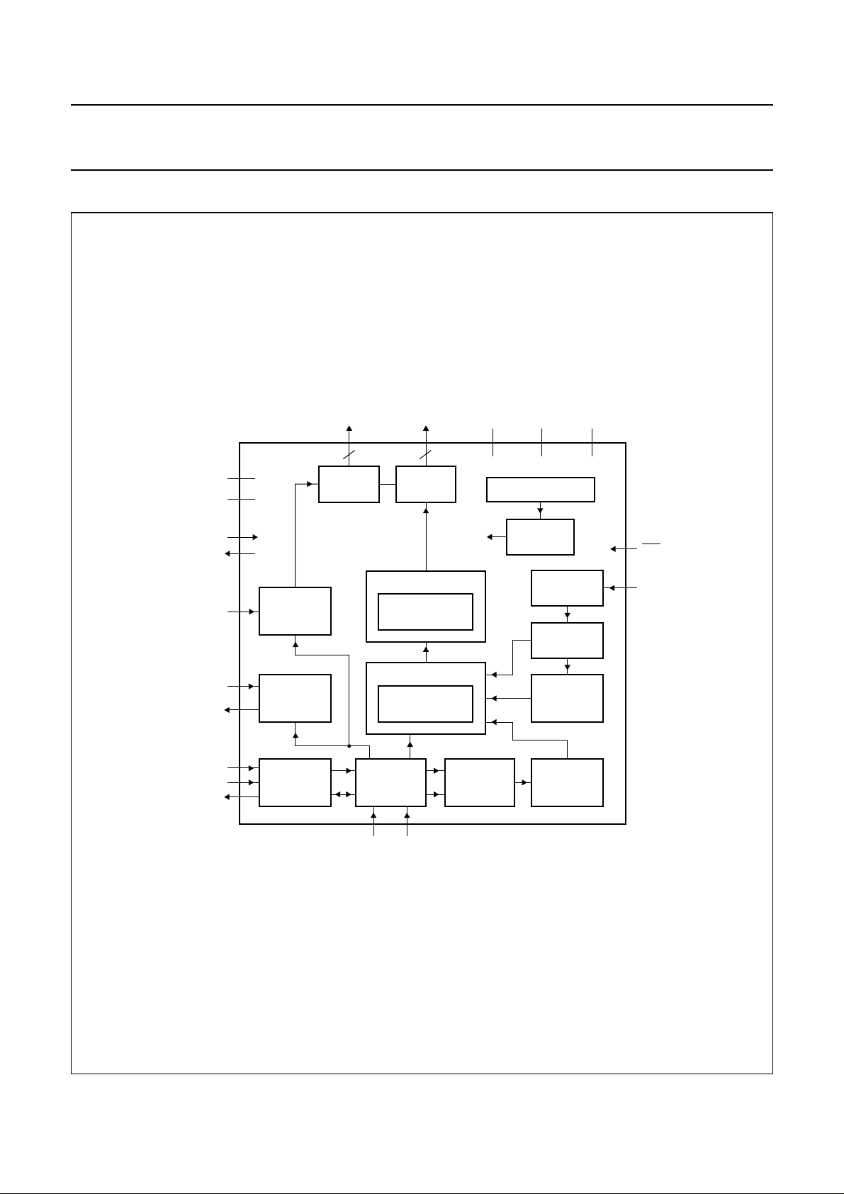
5 BLOCK DIAGRAM
handbook, full pagewidth
V
V
T4, T5
T1, T2, T3
V
LCDIN
V
LCDSENSE
V
LCDOUT
SDAOUT
SS1
SS2
SCL
SDA
BIAS
VOLTAGE
GENERATOR
V
LCD
GENERATOR
INPUT
FILTERS
R0 to R64
65
ROW
DRIVERS
PCF8535
C0 to C132
133
COLUMN
DRIVERS
DATA LATCHES
MATRIX
LATCHES
DISPLAY DATA RAM
MATRIX DATA
RAM
I2C-BUS
CONTROL
V
DD1
POWER-ON RESET
COMMAND
DECODER
V
DD2
INTERNAL
RESET
OSCILLATOR
TIMING
GENERATOR
DISPLAY
ADDRESS
COUNTER
ADDRESS
COUNTER
V
DD3
RES
OSC
SA0
SA1
Fig.1 Block diagram.
1999 Aug 24 4
MGS669
Page 5

Philips Semiconductors Objective specification
65 × 133 pixel matrix driver PCF8535
5.1 Block diagram functions
5.1.1 OSCILLATOR The on-chip oscillator provides the display clock for the
system; it requires no externalcomponents. Alternatively,
an external display clock may be provided via the OSC
input. The OSC input must be connected to V
DD1
or V
SS1
when not in use. During power-down additional current
saving can be made if the external clock is disabled.
5.1.2 POWER-ON RESET The on-chip Power-on reset initializes the chip after
power-on or power failure.
2
5.1.3 I
C-BUS CONTROLLER
The I2C-bus controller detects the I2C-bus protocol, slave
address, commands and display data bytes. It performs
the conversion of the data input (serial-to-parallel).
The PCF8535 acts as an I2C-bus slave and therefore
cannot initiate bus communication.
5.1.4 INPUT FILTERS Input filters are provided to enhance noise immunity in
electrically adverse environments; RC low-pass filters are
provided on the SDA, SCL and RES lines.
5.1.5 D
ISPLAY DATA RAM
The PCF8535 contains a 65 × 133 bit static RAM which
storesthe display data. The RAM is dividedinto9 banks of
133 bytes. The last bank is used for icon data and is only
one bit deep. During RAM access, data is transferred to
the RAM via the I2C-bus interface. There is a direct
correspondence between the X address and the column
output number.
5.1.6 TIMING GENERATOR The timing generator produces the various signals
required to drive the internal circuitry. Internal chip
operation is not disturbed by operations on the data bus.
5.1.7 ADDRESS COUNTER TheAddressCounter(AC)sendsaddressestotheDisplay
Data RAM (DDRAM) for writing.
5.1.8 DISPLAY ADDRESS COUNTER The display is generated by continuously shifting rows of
RAM data to the dot matrix LCD via the column outputs.
The display status (all dots on or off, normal or inverse
video) is set via the I2C-bus.
1999 Aug 24 5
Page 6

Philips Semiconductors Objective specification
65 × 133 pixel matrix driver PCF8535
6 PINNING
SYMBOL PAD DESCRIPTION
1 dummy pad
2 bump/alignment mark 1
R0 to R15 3 to 18 LCD row driver outputs
C0 to C132 19 to 151 LCD column driver outputs
R47 to R33 152 to 166 LCD row driver outputs
167 bump/alignment mark 2
168 dummy pad
R48 to R64 169 to 185 LCD row driver outputs; R64 is icon row
186 bump/alignment mark 3
187 to 189 dummy pad
OSC 190 oscillator
V
LCDIN
V
LCDOUT
V
LCDSENSE
RES 207 external reset input (active LOW)
T3 208 test output 3
T2 209 test output 2
T1 210 test output 1
V
DD2
V
DD3
V
DD1
SDA 230 and 231 I2C-bus serial data inputs
SDAOUT 232 I2C-bus serial data output
SA1 233 I2C-bus slave address input
SA0 234 I2C-bus slave address input
V
SS2
V
SS1
T5 251 test input 5
T4 252 test input 4
SCL 254 and 255 I2C-bus serial clock inputs
R32 to R16 257 to 273 LCD row driver outputs
191 to 196 LCD supply voltage
197 to 203 voltage multiplier output
204 voltage multiplier regulation input (V
205 and 206 dummy pad
211 to 218 supply voltage 2
219 to 222 supply voltage 3
223 to 228 supply voltage 1
229 dummy pad
235 to 242 ground 2
243 to 250 ground 1
253 dummy pad
256 bump/alignment mark 4
LCD
)
6.1 Pin functions
6.1.1 R0 TO R64
These pads output the display row signals.
1999 Aug 24 6
Page 7
Philips Semiconductors Objective specification
65 × 133 pixel matrix driver PCF8535
6.1.2 C0 TO C132
These pads output the display column signals.
6.1.3 V
V
and V
SS1
6.1.4 V
V
is the logic supply. V
DD1
multiplier. For split power suppliesV
AND V
SS1
SS2
DD1
SS2
must be connected together.
TO V
DD3
and V
DD2
are for the voltage
DD3
and V
DD2
DD3
must be
connectedtogether.If only one supply voltage is available,
all three supplies must be connected together.
6.1.5 V
If, in the application, an external V
LCDOUT
is used, V
LCD
LCDOUT
must be left open-circuit; otherwise (if the internal voltage
multiplier is enabled) the chip may be damaged. V
should not be driven when V
is below its minimum
DD1
LCDOUT
allowed value otherwise a low impedance path between
V
LCDOUT
6.1.6 V
This is the V
If the internal V
V
LCDIN
driven when V
otherwisea low impedance path between V
and V
LCDIN
will exist.
SS1
supply for when an external V
LCD
generator is used, then V
LCD
must be connected together. V
is below its minimum allowed value,
DD1
should not be
LCDIN
LCDIN
is used.
LCD
LCDOUT
andV
and
SS1
will exist.
and the Indium Tin Oxide (ITO) track resistance. It is
possible that during the acknowledge cycle the PCF8535
will not be able to create a valid logic 0 level. By splitting
the SDA input from the SDAOUT output the device could
be used in a mode that ignores the acknowledge bit.
In COG applications where the acknowledge cycle is
required or where read back is required, it is necessary to
minimizethetrackresistancefromtheSDAOUT pad to the
system SDA line to guarantee a valid LOW level.
6.1.10 SCL
2
C-bus serial clock input.
I
6.1.11 SA0 AND SA1
Least significant bits of the I2C-bus slave address.
Table 1 Slave address; see note 1
SA1 AND SA0 MODE SLAVE ADDRESS
0 and 0 write 78H
read 79H
0 and 1 write 7AH
read 7BH
1 and 0 write 7CH
read 7DH
1 and 1 write 7EH
read 7FH
6.1.7 V
LCDSENSE
This is the input to the internal voltage multiplier regulator.
It must be connected to V
LCDOUT
when the internal voltage
generator is used otherwise it may be left open-circuit.
V
LCDSENCE
should not be driven when V
is below its
DD1
minimum allowed value, otherwise a low impedance path
between V
LCDSENCE
and V
will exist.
SS1
6.1.8 SDA I2C-bus serial data input.
6.1.9 SDAOUT SDAOUT is the serial data acknowledge for the I2C-bus.
By connecting SDAOUT to SDA externally, the SDA line
becomes fully I2C-bus compatible. Having the
acknowledge output separated from the serial data line is
advantageous in Chip-On-Glass (COG) applications.
In COG applications where the track resistance from the
SDAOUT pad to the system SDA line can be significant, a
potential divider is generated by the bus pull-up resistor
1999 Aug 24 7
Note
1. The slave address is a concatination of the following
bits {01111, SA1, SA0 and R/W}.
6.1.12 OSC
If the on-chip oscillator is used this input must be
connected to V
DD1
or V
SS1
.
6.1.13 RES
External reset pad: when this pad is LOW the chip will be
reset; see Section 7.1. If an external reset is not required,
this pad must be tied to V
. Timing for the RES pad is
DD1
given in Chapter 12.
6.1.14 T1, T2, T3, T4 AND T5
In applications T4 and T5 must be connected to VSS.
T1, T2 and T3 are to be left open-circuit.
Page 8
Philips Semiconductors Objective specification
65 × 133 pixel matrix driver PCF8535
7 FUNCTIONAL DESCRIPTION
The PCF8535 is a low power LCD driver designed to interface with microprocessors/microcontrollers and a wide variety
of LCDs.
The host microprocessor/microcontroller and the PCF8535 are both connected to the I2C-bus. The SDA and SCL lines
must be connected to the positive power supply via pull-up resistors. The internal oscillator requires no external
components. The appropriate intermediate biasing voltage for the multiplexed LCD waveforms are generated on-chip.
The only other connections required to complete the system are to the power supplies (VDD,VSSand V
capacitors for decoupling V
LCD
and VDD.
) and suitable
LCD
handbook, full pagewidth
V
to V
DD1
V
DD(I2C)
V
SS1, VSS2
DD3
RES
SA0
SA1
SCL
SDA
V
LCD
DD2
DD1,VDD3
V
V
HOST
MICROPROCESSOR/
R
R
pu
pu
MICROCONTROLLER
V
SS
SS1VSS2
V
PCF8535
133 column drivers
65 row drivers
LCD PANEL
MGS670
Fig.2 Typical system configuration.
1999 Aug 24 8
Page 9

Philips Semiconductors Objective specification
65 × 133 pixel matrix driver PCF8535
7.1 Reset
The PCF8535 has two reset modes; internal Power-on
reset or external reset. Reset initiated from either the RES
pad or the internal Power-on reset block will initialize the
chip to the following starting condition:
• Power-down mode (PD = 1)
• Horizontal addressing (V = 0); no mirror X or Y
(MX = 0 and MY = 0)
• Display blank (D = 0 andE=0)
• Address counter X[6:0] = 0, Y[2:0] = 0 and XM0=0
• Bias system BS[2:0] = 0
• Multiplex rate M[2:0] = 0 (Mux rate1:17)
• Temperature control mode TC[2:0] = 0
• HV-gen control, HVE = 0 the HV generator is switched
off, PRS = 0 and S[1:0] = 00
• V
LCDOUT
is equal to 0 V
• RAM data is unchanged (Note: RAM data is undefined
after power-up)
• All row and column outputs are set to VSS (display off)
• TRS and BRS are set to zero
• Direct mode is disabled (DM = 0)
• Internal oscillator is selected, but not running (EC = 0)
• Bias current set to low current mode (IB = 0).
7.3 LCD voltage selector
The practical value for VOP is determined by equating
V
with defined LCD threshold voltage (Vth), typically
off(rms)
when the LCD exhibits approximately 10% contrast.
7.4 Oscillator
The internal logic operation and the multi-level drive
signals of the PCF8535 are clocked by the built-in RC
oscillator. No external components are required.
7.5 Timing
ThetimingofthePCF8535organizestheinternaldataflow
of the device. The timing also generates the LCD frame
frequency which is derived from the clock frequency
generated in the internal clock generator.
7.6 Column driver outputs
The LCD drive section includes 133 column outputs
(C0 to C132) which should be connected directly to the
LCD. The column output signals are generated in
accordance with the multiplexed row signals and with the
data in the display latch. When less than 133 columns are
required the unused column outputs should be left
open-circuit.
7.7 Row driver outputs
7.2 Power-down
During power-down all static currents are switched off (no
internal oscillator, no timing and no LCD segment drive
system) and all LCD outputs are internally connected to
VSS. The serial bus function remains active.
The LCD drive section includes 65 row outputs
(R0 to R64) which should be connected directly to the
LCD. The row output signals are generated in accordance
with the selected LCD drive mode. If lower Mux rates or
less than 65 rows are required, the unused outputs should
be left open-circuit.
1999 Aug 24 9
Page 10
Philips Semiconductors Objective specification
65 × 133 pixel matrix driver PCF8535
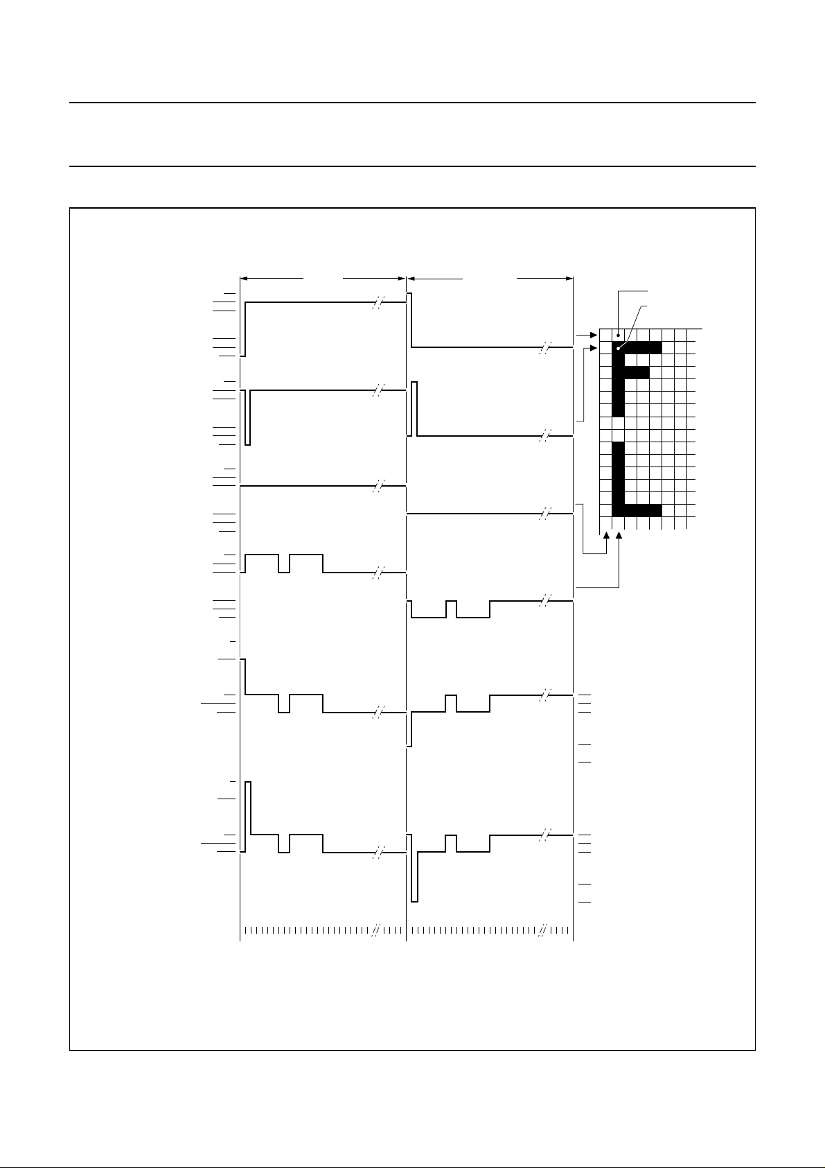
7.8 Drive waveforms
ROW 0
R0 (t)
ROW 1
R1 (t)
COL 0
C0 (t)
COL 1
C1 (t)
V
LCD
V3 − V
V
V
V
V
V
V
V
V
V
V
V
V
V
V
V
V
V
V
V
V
V
V
V
V
LCD
2
3
4
5
SS
LCD
2
3
4
5
SS
LCD
2
3
4
5
SS
LCD
2
3
4
5
SS
− V
SS
SS
frame n frame n + 1
V
state1
V
state2
(t)
(t)
V
− V
LCD
V
V
V
(t) = C1(t) − R0(t).
state1
V
(t) = C1(t) − R1(t).
state2
state1
state2
(t)
(t)
0 V
V3 − V
V
LCD
V3 − V
V
LCD
0 V
V3 − V
2
SS
− V
SS
SS
− V
2
SS
012345678... ... 64 01234567 8... ... 64
Fig.3 Typical LCD driver waveforms.
1999 Aug 24 10
V4 − V
0 V
VSS − V
V4 − V
V
− V
SS
V4 − V
0 V
VSS − V
V4 − V
V
− V
SS
MGS671
5
5
LCD
LCD
5
5
LCD
LCD
Page 11
Philips Semiconductors Objective specification
65 × 133 pixel matrix driver PCF8535
7.9 Set multiplex rate
The PCF8535 can be used to drive displays of varying sizes. The multiplex mode selected controls which rows are used.
In all cases, the last row is always driven and is intended for icons. If Top Row Swap (TRS) is at logic 1 then the icon row
will be output on pad R48. M[2:0] selects the multiplex rate (see Table 2).
Table 2 Multiplex rates
M[2] M[1] M[0] MULTIPLEX RATE ACTIVE ROWS
0 0 0 1 : 17 R0 to R15 and R64
0 0 1 1 : 26 R0 to R24 and R64
0 1 0 1 : 34 R0 to R32 and R64
0 1 1 1 : 49 R0 to R47 and R64
1 0 0 1:65 R0toR64
101 − 111 do not use −
7.10 Bias system
7.10.1 SET BIAS SYSTEM
The bias voltage levels are set in the ratio of R − R − nR − R − R. Differentmultiplex rates require differentfactors n. This
is programmed by BS[2:0]. For optimum bias values, n can be calculated from:
n Mux rate 3–=
Changing the bias system from the optimum will have a consequence on the contrast and viewing angle. One reason to
come away from the optimum would be to reduce the required V
. A compromise between contrast and VOP must be
OP
found for any particular application.
Table 3 Programming the required bias system
BS[2] BS[1] BS[0] n BIAS MODE TYPICAL MUX RATES
00071/
00161/
01051/
01141/
10031/
10121/
11011/
1110
11
10
9
8
7
6
5
1
/
4
1 : 100
1:80
1:65
1:49
1:33
1:26
1:17
1:9
1999 Aug 24 11
Page 12

Philips Semiconductors Objective specification
65 × 133 pixel matrix driver PCF8535
Table 4 Example of LCD bias voltage for1/7bias, n = 3
1
SYMBOL BIAS VOLTAGE FOR
V1 V
V2
V3
V4
V5
V6 V
6
/7× V
5
/7× V
2
/7× V
1
/7× V
LCD
SS
/7BIAS
LCD
LCD
LCD
LCD
7.11 Temperature measurement
7.11.1 T
EMPERATURE READ BACK
The PCF8535 has an in-built temperature sensor.
For power saving, the sensor should only be enabled
when a measurement is required. It will not operate in
power-down mode. The temperature read back requires a
clock to operate. Normally the internal clock is used but, if
the device is operating from an external clock, then this
must be present for the measurement to work. V
V
mustalso be applied. A measurement is initialized by
DD3
DD2
and
setting the SM bit. Once started the SM bit will be
automatically cleared. An internal oscillator will be
initialized and allowed to warm-up for approximately
2 frame periods. After this the measurement starts and
lasts for a maximum of 2 frame periods.
Temperature data is returned via a status register. During
the measurement the register will contain zero. Once the
measurement is completed the register will be updated
with the current temperature (non zero value). Because
the I2C-bus interface is asynchronous to the temperature
measurement, read back prior to the end of the
measurement is not guaranteed. If this mode is required
the register should be read twice to validate the data.
For calibrating the temperature read-out a measurement
must be taken at a defined temperature. The offset
between the ideal read-out and the actual result has to be
stored into a non-volatile register (e.g. EEPROM);
Offset TR
where TR
meas
TR
–=
ideal
meas
is the actual temperature read-out of the
(2)
PCF8535.
The calibrated temperature read-out can be calculated for
each measurement as follows:
TR
cal
TR
meas
Offset+=
(3)
The accuracy after the calibration is ±6.7% (plus ±1 lsb) of
the difference between the current temperature and the
calibration temperature. For this reason a calibration at or
near the most sensitive temperature for the display is
recommended.
E.g. for a calibration at 25 °C with the current temperature
at −20 °C, the absolute error may be calculated as:
Absolute error = 0.067 × (25 °C −−20 °C)
= ±3 °C+±1 lsb = ±4.17 °C.
7.12 Temperature compensation
7.12.1 TEMPERATURE COEFFICIENTS Due to the temperature dependency of the liquid crystals
viscosity the LCD controlling voltage,V must be increased
at lower temperatures to maintain optimum contrast.
Figure 4 shows V
as a function of temperature for a
LCD
typical high multiplex rate liquid.
Inthe PCF8535 the temperature coefficient of V
LCD
canbe
selected from 8 values by setting bits TC[2:0],
see Table 5.
The ideal temperature read-out can be calculated as
follows;
TR
128 T 27 °C–()
ideal
×+=
-- c
(1)
1
where T is the on-chip temperature in °C and c is the
conversion constant; c = 1.17 °C/lsb.
Toimprove the accuracy of the temperature measurement
a calibration is recommended during the assembly of the
final product.
1999 Aug 24 12
Page 13
Philips Semiconductors Objective specification
65 × 133 pixel matrix driver PCF8535
handbook, halfpage
V
LCD
Fig.4 V
as function of liquid crystal temperature (typical values).
LCD
Table 5 Selectable temperature coefficients
TC[2] TC[1] TC[0] TC VALUE UNIT
000 0 1/°C
001−0.44 × 10
010−1.10 × 10
011−1.45 × 10
100−1.91 × 10
101−2.15 × 10
110−2.32 × 10
111−2.74 × 10
7.13 V
7.13.1 SET V
OP
OP
VALUE
−3
−3
−3
−3
−3
−3
−3
1/°C
1/°C
1/°C
1/°C
1/°C
1/°C
1/°C
The voltage at the reference temperature can be
calculated as: [V
V
LCD
Tcut()
The operating voltage, V
(T=T
LCD
aVOPb×+()=
)]
cut
, can be set by software.
OP
(4)
The generated voltage is dependent on the temperature,
programmed Temperature Coefficient (TC) and the
programmed voltage at the reference temperature (T
V
LCD
aVOPb×+()1TT
The values for T
, a and b are given in Table 6.
cut
–()TC×()+()×=
cut
cut
):
(5)
The maximumvoltagethatcan be generated is dependent
on the voltage V
and the display load current.
DD2
Two overlapping VOP ranges are selectable via the
command page “Hv-gen control”, see Fig.5.
MGS473
0 °C
T
The low range offers programming from 4.5 to 10.215 V,
with the high range from 10.215 to 15.93 V at the cut point
temperature, T
. Care must be taken, when using
cut
temperature coefficients, that the programmed voltage
does not exceed the maximum allowed V
LCD
voltage,
see Chapter 10.
Fora particular liquid, the optimumV
canbe calculated
LCD
for a given multiplex rate. For a Mux rate of 1 : 65, the
optimum operating voltage of the liquid can be calculated
as:
V
LCD
where V
165+
---------------------------------------
×
–
21
is the threshold voltage of the liquid crystal
th
----------
1
65
V
× 6.85 Vth×==
th
material used.
Table 6 Values for parameters of the HV generator
programming
SYMBOL BITS VALUE UNIT
a PRS = 0 4.5 V
PRS = 1 10.215 V b 0.045 V T
cut
27 °C
(6)
1999 Aug 24 13
Page 14
Philips Semiconductors Objective specification
65 × 133 pixel matrix driver PCF8535
handbook, full pagewidth
V
LCD
b
a
00 01 02
VOP[6:0] programming (00H to 7FH, programming range LOWand HIGH).
03 04 05 06 . . . 5F 6F 7F 00 01 02 03 04 05 06 . . . 5F 6F 7F
LOW HIGH
Fig.5 VOP programming of PCF8535.
7.14 Voltage multiplier control
7.14.1 S[1:0] The PCF8535 incorporates a software configurable
voltage multiplier. After reset (RES) the voltage multiplier
is set to 2 × V
. Other voltage multiplier factors are set
DD2
via the HV-gen command page. Before switching on the
charge pump, the charge pump has to be pre-charged
using the following sequence.
A starting state of HVE = 0, DOF = 0, PD = 1 and DM = 0
is assumed. A small delay between steps is indicated.
The recommended wait period is 20 µs per 100 nF of
capacitance on V
LCD1
.
1. Set DM = 1 and PD = 0
2. Delay
3. Set the multiplication factor to 2 by setting S[1:0] = 00
4. Set the required VOP and PRS.
5. Set HVE = 1 to switch-on the charge pump with a
multiplication factor of 2
6. Delay
7. Increase the number of stages, one at a time, with a
delay between each until the required level is
achieved.
MGS472
Table 7 HV generator multiplication factor
S[1] S[0] MULTIPLICATION FACTOR
00 2× V
01 3× V
10 4× V
11 5× V
DD2
DD2
DD2
DD2
1999 Aug 24 14
Page 15
Philips Semiconductors Objective specification
65 × 133 pixel matrix driver PCF8535
7.15 Addressing
Addressing of the RAM can be split into two parts; input
addressing and output addressing. Input addressing is
concerned with writing data into the RAM. Output
addressing is almost entirely automatic and taken care of
by the device, however, it is possible to affect the output
mode.
7.15.1 INPUT ADDRESSING
Data is down loaded byte wise into the RAM matrix of the
PCF8535 as indicated in Figs 6 to 10.
Table 8 Effect of X-RAM page pointer
X ADDRESS POINTER
X-RAM PAGE POINTER
XM
0
0 0 C0 C132 1 0 C1 C131 2 0 C2 C130
:::: 125 0 C125 C7 126 0 C126 C6 127 0 C127 C5
0 1 C128 C4 1 1 C129 C3
::::
4 1 C132 C0
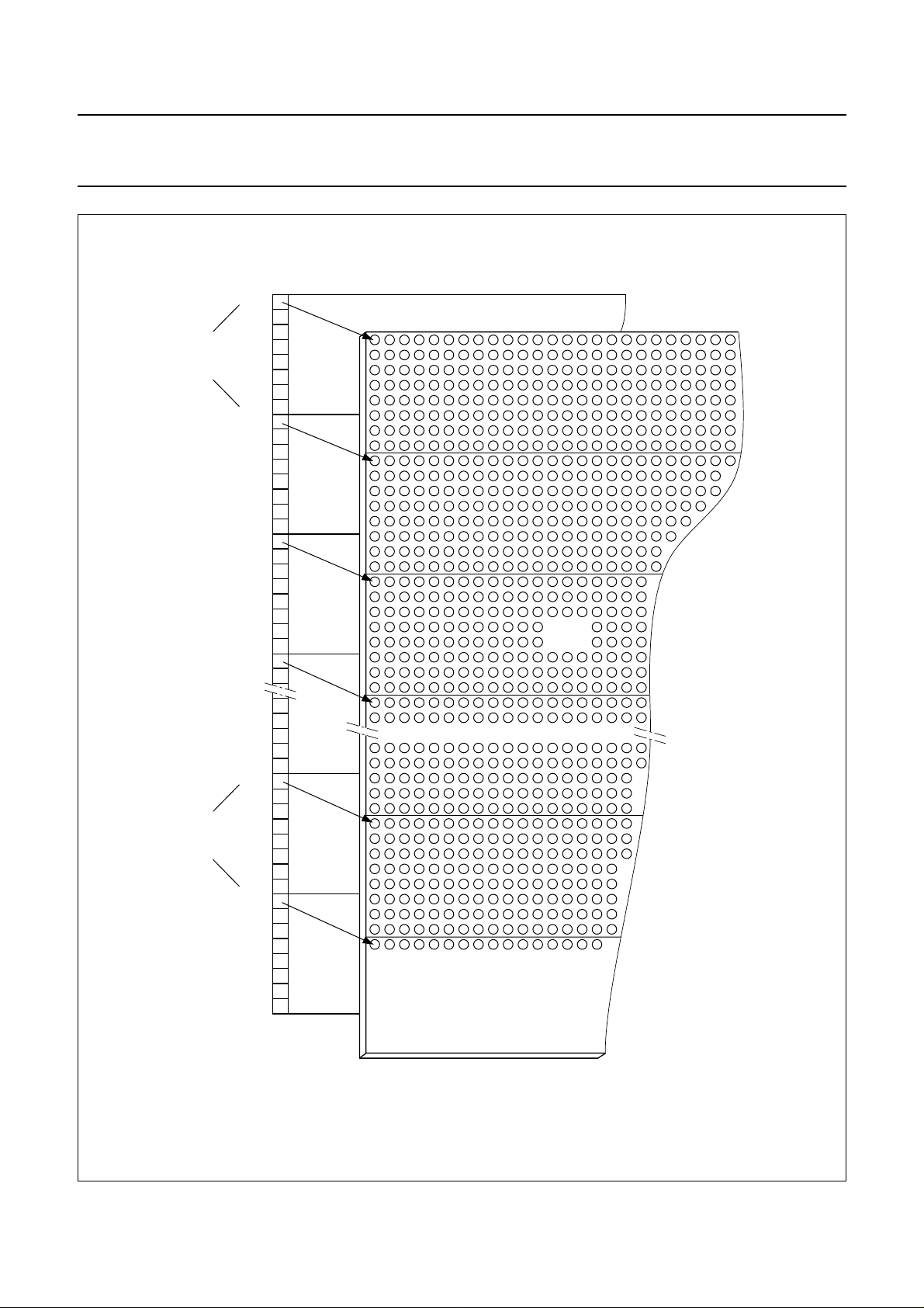
The display RAM has a matrix of 65 × 133 bits.
The columns are addressed by a combination of the
X address pointer and the X-RAM page pointer, whilst the
rows addressed in groups of 8 by the Y address pointer.
The X address pointer has a range of 0 to 127 (7FH).
Its range can be extended by the X-RAM page pointer,
XM0. The Y address pointer has a range of 0 to 8 (08H).
The PCF8535 is limited to 133 columns by 65 rows,
addressing the RAM outside of this area is not allowed.
ADDRESSED COLUMN
MX = 0
ADDRESSED COLUMN
MX = 1
Banks 1 to 7 use
the entire byte
handbook, full pagewidth
MSB
LSB
Bank 8 is only
1 bit deep and
uses the MSB
MSB
LSB
01234
icon data
56789
101112131415161718192021222324
Fig.6 RAM format, input addressing.
1999 Aug 24 15
.. .. .. ..
X address
XM0 = 1XM0 = 0
0
1
2
3
4
5
Y address
6
7
8
119
123
120
121
122
124
125
126
127
01234
MGS673
Page 16
Philips Semiconductors Objective specification
65 × 133 pixel matrix driver PCF8535
Data byte in location
X = 0, Y = 0, MX0 = 0
(MX = 0, MY = 0)
MSB
LSB
bank 0
top of LCD
R0
bank 1
R8
bank 2
R16
LCD
bank 3
R24
MSB
Data byte in location
Y = 7, X = 0, MX0 = 0
(MX = 0, MY = 0)
LSB
bank 7
bank 8
Fig.7 DDRAM to display mapping.
1999 Aug 24 16
R56
R64
MGS674
Page 17

Philips Semiconductors Objective specification
65 × 133 pixel matrix driver PCF8535
Two automated addressing modes are available; vertical
addressing (V = 1) and horizontal addressing (V = 0).
These modes change the way in which the
auto-incrementing of the address pointers is handled and
are independent of multiplex rate. The auto-incrementing
works in a way so as to aid filling of the entire RAM. It is
not a prerequisite of operation that the entire RAM is filled;
inlowermultiplex modes not all of the RAM will beneeded.
For these multiplex rates, use of horizontal addressing
mode (V = 0) is recommended.
Addressing the icon row is a special case as these RAM
locations are not automatically accessed. These locations
must be explicitly addressed by setting the Y address
pointer to 8.
The Y address pointer does not auto-increment when the
X address over or underflows, it stays set to 8. Writing
icon data is independent of the vertical and horizontal
addressing mode, but is effected by the mirror X bit as
described in Sections 7.15.1.2 and 7.15.1.3.
The addressing modes may be further modified by the
mirror X bit MX. This bit causes the data to be written into
the RAM from right to left insteadof the normal left to right.
This effectively flips the display about the Y axis. The MX
bit affects the mode of writing into the RAM, changing the
MX bit after RAM data is written will not flip the display.
7.15.1.1 Vertical addressing: non-mirrored;
V = 1 and MX = 0
In the vertical addressing mode data is written top to
bottom and left to right. Here, the Y counter will
auto-incrementfrom0 to 7 and then wrap around to 0 (see
Fig.8). On each wrap over, the X counter will increment to
address the next column. When the X counter wraps over
from 127 to 0, the XM0 bit will be set. The last address
accessible is Y = 7, X = 4 and XM0= 1; after this access
the counter will wrap around to Y = 0, X = 0 and XM0=0.
handbook, full pagewidth
byte number
byte order for
icon data
Fig.8 Sequence of writing data bytes into the RAM with normal vertical addressing (V = 1 and MX = 0).
26 25 24
....
15 14 13 12 11 10 9 8
23 22 21 20 19 18 17 16
076543210
1
2
01234
icon data
56789
12131415161718192021222324
101112131415161718192021222324
.... ....
X address
XM0 = 1XM0 = 0
1035 1034 1033 1032
....
....
1060
1061
1062
0
1
2
3
4
5
Y address
6
....
1012
1013
1014
1016
1017
1018
1019
1020
1021
1022
1024
1025
1026
1027
1028
1029
1030
7
1031
128
129
130
131
01234
1063
132
8
MGS675
1015
1023
119
123
124
125
122
122
123
124
125
126
126
127
127
120
121
119
120
121
1999 Aug 24 17
Page 18

Philips Semiconductors Objective specification
65 × 133 pixel matrix driver PCF8535
7.15.1.2 Vertical addressing: mirrored; V = 1 and MX = 1
It is also possible to write data from right to left, instead of from the normal left to right, still going top to bottom. In the
mirrored vertical addressing mode the Y counter will auto-increment from 0 to 7 and then wrap around to 0 (see Fig.9).
On each wrap-over, the X counter will decrement to address the preceding column. The XM0 bit will be automatically
toggled each time the X address counter wraps over from 0. The last address accessible is Y = 7, X = 0 and XM0=0;
after this access the counter will wrap around to Y = 0, X = 4 and XM0=1.
handbook, full pagewidth
byte number
byte order for
icon data
....
1053 1052
1054
1055
132 1063 1062 1061 1060 1059 1058 1057 1056
131
130
01234
icon data
56789
119
118
117
116
120
101112131415161718192021222324
111
115
114
113
112
110
109
108
.... ....
13
119
121110
120
121
122
987
123
124
125
48
50 49
....
6
126
XM0 = 1XM0 = 0
32
40
33
41
34
42
35
43
36
44
37
45
....
38
30
46
39
31747
43210
5
01234
127
X address
Fig.9 Sequence of writing data bytes into the RAM with mirrored vertical addressing (V = 1 and MX = 1).
....
8
9
10
0
0
1
1
2
3
432
4
5
5
6
6
7
8
Y address
MGS676
1999 Aug 24 18
Page 19

Philips Semiconductors Objective specification
65 × 133 pixel matrix driver PCF8535
7.15.1.3 Horizontal addressing: non-mirrored; V = 0 and MX = 0
In horizontal addressing mode data is written from left to right and top to bottom. Here, the X counter will auto-increment
from 0 to 127, set the XM0, then count 0 to 4 before wrapping around to 0 and clearing the XM0bit (see Fig.10). On each
wrap-over, the Y counter will increment. The last address accessible is Y = 7, X = 4 and XM0= 1; after this access the
counter will wrap around to Y = 0, X = 0 and XM0=0.
handbook, full pagewidth
124
1055
124
124
125
....
1056
125
125
126
924
1057
126
126
127
925
1058
127
127
XM0 = 1XM0 = 0
128
129
130
131
927
928
929
926
1059
1060
1061
1062
128
129
130
131
01234
132
930
1063
132
byte number
byte order for
icon data
2
3456789
136
934
932 1341933 135
0 931 133 0
1
2
01234
....
935
936
icon data
56789
101112131415161718192021222324
937
938
939
940
941
942
943
944
945
946
12131415161718192021222324
11
10
12131415161718192021222324
947
948
949
950
951
952
953
954
955
.... ....
119
1050
119
119
120
1051
120
120
121
1052
121
121
122
1053
122
122
123
1054
123
123
X address
Fig.10 Sequence of writing data bytes into the RAM with normal horizontal addressing (V = 0 and MX = 0).
0
1
2
3
4
5
6
7
8
Y address
MGS677
1999 Aug 24 19
Page 20

Philips Semiconductors Objective specification
65 × 133 pixel matrix driver PCF8535
7.15.1.4 Horizontal addressing: mirrored; V = 0 and MX = 1
It is also possible to write data from right to left, instead of from the normal left to right, still going top to bottom. In the
mirrored horizontal addressing mode the X counter will auto-decrement from 4 to 0, clear the XM0, then count 127 to 0
before wrapping around to 4 and setting the XM0 bit (see Fig.10). On each wrap-over, the Y counter will increment.
The last address accessible is Y = 7, X = 0 and XM0= 0; after this access the counter will wrap around to Y = 0, X = 4
and XM0=1.
handbook, full pagewidth
939
124
938
125
937
6
126
56789
936
5
127
XM0 = 1XM0 = 0
4
321
....
136
135
935
934
933
43210
01234
134
932
0
133
931
byte number
byte order for
icon data
130
129
131
929
928
927
1060
1062
1061
132 1063 930 132
131
130
01234
128
127
126
926
925
924
1059
1058
1057
icon data
56789
119
118
117
116
125
124
123
122
121
120
115
....
1056
1055
1054
1053
1052
1051
1050
1049
1048
1047
1046
119
118
117
116
120
101112131415161718192021222324
115
114
1045
114
113
1044
113
112
1043
112
111
110
109
108
1042
1041
1040
1039
111
110
109
108
.... ....
13
944
13
119
11
12
942
943
121110
120
121
10
941
122
940
987
123
X address
Fig.11 Sequence of writing data bytes into the RAM with mirrored horizontal addressing (V = 0 and MX = 1).
0
1
2
3
4
5
6
7
8
MGS678
Y address
1999 Aug 24 20
Page 21

Philips Semiconductors Objective specification
65 × 133 pixel matrix driver PCF8535
7.15.2 OUTPUT ADDRESSING The output addressing of the RAM is done automatically in accordance with the currently selected multiplex rate.
Normally the user would not need to make any alterations to the addressing. There are, however, circumstances
pertainingtovarious connectivity of the device on a glassthatwouldbenefit from some in-built functionality. Three modes
exist that enable the user to modify the output addressing, namely:
1. MY, mirror the Y axis. This mode effectively flips the display about the X axis, resulting in an upside down display.
Theeffect is observable immediately the bit ismodified. This is useful if thedeviceis to be mounted above thedisplay
area instead of below.
2. Bottom Row Swap (BRS). This mode swaps the order of the rows on the bottom
aide routing to the display when it is not possible to pass tracks under the device; a typical example would be in tape
carrier package. This mode is often used in conjunction with TRS.
3. Top Row Swap (TRS). As with BRS, but swaps the order of rows on the top
7.15.2.1 Mirror Y, MY
As described above, the Y axis is mirrored in the X axis.
(1)
edge of the chip. This is useful to
(1)
edge of the chip.
handbook, full pagewidth
MY = 0
Mirror
MY = 1
Y axis
Y axis
C0C1C2C3C4C5C6C7C8C9C10
R0
R1
R2
R3
R4
R5
R6
R7
R8
....
R64
R55
R56
R57
R58
R59
R60
R61
R62
R63
R64
... icons ...
... icons ...
C11
C12
C13
C14
C15
C16
C17
C18
C19
C20
C21
C22
C23
C24
C25
C26
MGS679
C27
..
C28
Fig.12 Mirror Y behaviour (Mux rate 1 : 65).
(1) The top edge is defined as the edge containing the user interface connections. The bottom edge is the opposing edge.
1999 Aug 24 21
Page 22

Philips Semiconductors Objective specification
65 × 133 pixel matrix driver PCF8535
7.15.2.2 Bottom Row Swap
Here the order of the row pads is modified. Each block of rows is swapped about its local Y axis.
handbook, full pagewidth
R16 R32 R64 R48
INTERFACE
COLUMNS
R15 R0
R33 R47
Fig.13 Bottom row swap.
7.15.2.3 Top Row Swap
Here the order of the row pads is modified. Each block of rows is swapped about its local Y axis.
MGS680
handbook, full pagewidth
R32 R16 R48 R64
INTERFACE
COLUMNS
R0 R15
Fig.14 Top row swap.
1999 Aug 24 22
R47 R33
MGS681
Page 23

Philips Semiconductors Objective specification
65 × 133 pixel matrix driver PCF8535
7.15.2.4 Output row order
The order in which the rows are activated is a function of bits MY, TRS, BRS and the selected multiplex mode.
Tables 9 to 12 give the order in which the rows are activated. In all cases, the RAM is accessed in a linear fashion,
starting at zero with a jump to the last row for the icon data.
Table 9 Row order for BRS = 0 and TRS = 0
MULTIPLEX MODE MY = 0 MY = 1
1 : 17 R0 to R15 and R64 R15 to R0 and R64
1 : 26 R0 to R24 and R64 R24 to R0 and R64
1 : 33 R0 to R31 and R64 R31 to R0 and R64
1 : 49 R0 to R47 and R64 R47 to R0 and R64
1 : 65 R0 to R64 R63 to R0 and R64
Table 10 Row order for BRS = 1 and TRS = 0
MULTIPLEX MODE MY = 0 MY = 1
1 : 17 R15 to R0 and R64 R0 to R15 and R64
1 : 26 R15 to R0, R16 to R24 and R64 R24 to R16, R0 to R15 and R64
1 : 33 R15 to R0, R16 to R31 and R64 R31 to R16, R0 to R15 and R64
1 : 49 R15 to R0, R16 to R32, R47 to R33
and R64
1 : 65 R15 to R0, R16 to R32, R47 to R33
and R48 to R64
R33 to R47, R32 to R16, R0 to R15
and R64
R63 to R48, R33 to R47, R32 to R16,
R0 to R15 and R64
Table 11 Row order for BRS = 0 and TRS = 1
MULTIPLEX MODE MY = 0 MY = 1
1 : 17 R0 to R15 and R48 R15 to R0 and R48
1 : 26 R0 to R15, R32 to R24 and R48 R24 to R32, R15 to R0 and R48
1 : 33 R0 to R15, R32 to R17 and R48 R17 to R32, R15 to R0 and R48
1 : 49 R0 to R15, R32 to R16, R33 to R47
and R48
1 : 65 R0 to R15, R32 to R16, R33 to R47
and R64 to R48
Table 12 Row order for BRS = 1 and TRS = 1
MULTIPLEX MODE MY = 0 MY = 1
1 : 17 R15 to R0 and R48 R0 to R15 and R48
1 : 26 R15 to R0, R32 to R24 and R48 R0 to R15, R32 to R24 and R48
1 : 33 R15 to R0, R32 to R17 and R48 R0 to R15, R17 to R32 and R48
1 : 49 R15 to R0, R32 to R16, R47 to R33
and R48
1 : 65 R15 to R0, R32 to R16, R47 to R33
and R64 to R48
R47 to R33, R16 to R32, R15 to R0
and R48
R49 to R64, R47 to R33, R16 to R32,
R15 to R0 and R48
R0 to R15, R16 to R32, R33 to R47
and R48
R0 to R15, R16 to R32, R33 to R47,
R47 to R64 and R48
1999 Aug 24 23
Page 24

Philips Semiconductors Objective specification
65 × 133 pixel matrix driver PCF8535
7.16 Instruction set
Data accesses to the PCF8535 can be broken down into
two areas, those that define the operating mode of the
device and those that fill the display RAM; the distinction
being the D/C bit. When the D/C bit is at logic 0, the chip
will respond to instructions as defined in Table 16. When
the D/C bit is at logic 1, the chip will store data into the
RAM. Data may be written to the chip that is independent
to the presence of the display clock.
There are 4 instruction types. Those which:
1. Define PCF8535 functions such as display configuration, etc.
2. Set internal RAM addresses
3. Perform data transfer with internal RAM
4. Others.
In normal use, category 3 instructions are the most
frequently used. To lessen the MPU program load,
automatic incrementing by one of the internal RAM
address pointers after each data write is implemented.
The instruction set is broken down into several pages,
each command page being individually addressed via the
H[2:0] bits.
7.16.1 RAM READ/WRITE COMMAND PAGE
This page is special in that it is accessible independently
of the H bits. This page is mainly used as a stepping stone
to other pages. Sending the ‘Default H[2:0]’ command will
cause an immediate step to the ‘Function and RAM
command page’ which will allow the H[2:0] bits to be set.
7.16.2 FUNCTION AND RAM COMMAND PAGE
7.16.2.1 Command page
Setting H[2:0] will move the user immediately to the
required command page. Pages not listed should not be
accessed as the behaviour is not defined.
• Oscillator off
• V
• I2C-bus interface accesses are possible
• RAM contents are not cleared; RAM data can be written
• Register settings remain unchanged.
V
When V = 0, horizontal addressing is selected. When
V = 1, vertical addressing is selected. The behaviour is
described in Section 7.15.
may be disconnected
LCDIN
7.16.2.3 RAM page
The XM0bit extends the RAM into a second page. The bit
may be considered to be the Most Significant Bit (MSB) of
an 8-bit X address. The behaviour is described in
Section 7.15.
7.16.2.4 Set Yaddress
The Y address is used as a pointer to the RAM for RAM
writing. The range is 0 to 8. Each bank corresponds to a
set of 8 rows, the only exception being bank 8, which
contains the icon data and is only 1-bit deep;see Table 13.
Table 13 Yaddress pointer
Y[3] Y[2] Y[1] Y[0] BANK ROWS
0000bank 0 R0 to R7
0001bank 1 R8 to R15
0010bank 2 R16 to R23
0011bank 3 R24 to R31
0100bank 4 R32 to R39
0101bank 5 R40 to R47
0110bank 6 R48 to R55
0111bank 7 R56 to R63
1000bank 8
(icons)
R64
7.16.2.2 Function set
PD
When PD = 1, the LCD driver is in power-down mode:
• All LCD outputs at V
1999 Aug 24 24
SS
Page 25

Philips Semiconductors Objective specification
65 × 133 pixel matrix driver PCF8535
7.16.2.5 Set X address
The X address is used as a pointer to the RAM for RAM
writing. The range of X is 0 to 127 (7FH) and may be
extended by the XM0bit. The combined value of XM0and
X address directly corresponds to the display column
number when MX = 0 and corresponds to the inverse
display column number when MX = 1; see Table 14.
Table 14 X address pointer
XM
, X[6:0]
0
0 C0 C132 1 C1 C131 2 C2 C130 3 C3 C129
:: : 129 C129 C3 130 C130 C2 131 C131 C1 132 C132 C0
7.16.3 DISPLAY SETTING COMMAND PAGE
ADDRESSED
COLUMN, MX = 0
ADDRESSED
COLUMN, MX = 1
7.16.3.1 Display control
7.16.3.3 Bias system
BS[2:0] sets the bias system; see Section 7.10.
7.16.3.4 Display size
Physically large displays require stronger drivers. Bit IB
enables the user to select a stronger driving mode and
should be used if suitable display quality can not be
achieved with the default setting.
7.16.3.5 Multiplex rate
M[2:0] sets the multiplex rate; see Section 7.9.
7.16.4 HV-GEN COMMAND PAGE
7.16.4.1 HV-gen control
PRS
Programmable charge pump range select. This bit defines
whether the programmed voltage for VOP is in the low or
the high range. The behaviour of this bit is further
described in Section 7.13.
HVE
High voltage generator enable. When set to logic 0, the
charge pump is disabled. When set to logic 1, the charge
pump is enabled.
The D and E bits set the display mode as given in
Table 15.
Table 15 Display control
D E MODE
0 0 display blank 1 0 normal mode 0 1 all display segments on 1 1 inverse video
7.16.3.2 External display control
Mirror X and mirror Y have the effect of flipping the display
left to right or top to bottom respectively. MX works by
changing the order data that is written into the RAM.
As such, the effects of toggling MX will only be seen after
data is written into the RAM. MY works by reversing the
order that column data is accessed relative to the row
outputs. The effect of toggling MY will be seen
immediately. The behaviour of both of these bits is further
described in Section 7.15.
7.16.4.2 HV-gen stages
S[1:0] set the multiplication factor of the charge pump
ranging from times 2 to times 5. The behaviour of these
bits is further described in Section 7.14.
7.16.4.3 Temperature coefficients
TC[2:0] set the required temperature coefficient.
The behaviour of these bits is further described in
Section 7.12.
7.16.4.4 Temperature measurement control
The SM bit is used to initiate a temperature measurement.
The SM bit is automatically cleared at the end of the
measurement. The behaviour of this bit is further
described in Section 7.11.
7.16.4.5 V
VOP[6:0] sets the required operating voltage for the
display.
LCD
control
1999 Aug 24 25
Page 26

Philips Semiconductors Objective specification
65 × 133 pixel matrix driver PCF8535
7.16.5 SPECIAL FEATURE COMMAND PAGE
7.16.5.1 State control
DM
Direct mode allows V
V
. This may be useful in systems where VDD is to be
DD2
used for V
LCD
.
to be sourced directly from
LCDOUT
DOF
Displayoffwillturnoffall internal analog circuitry that is not
required for temperature measurement.
As a consequence the display will be turned off. This
mode is only required if temperature measurements are
required whilst in power-down mode.
7.16.5.2 Oscillator setting
The internal oscillator may be disabled and the source
clock for the display derived from the OSC pad. It is
important to remember that LCDs are damaged by DC
voltages and that the clock, whether derived internally or
externally, should never be disabled whilst the display is
active. The internal oscillator is switched off during
power-down mode.
When using an external clock and disabling it during
power-down mode will further reduce the standby current.
If it is not possible to disable it externally then it is worth
notingthatbyselectingtheinternalclock,which is disabled
during power-down mode, the same effect may be
achieved.
7.16.5.3 COG/TCP
The chip may be mounted on either a glass, foil or tape
carrier package. For these applications, different
organizations of the row pads are required to negate the
necessity of routing under the device. The TRS and BRS
allowfor this swapping. The behaviour of bothofthese bits
is further described in Section 7.15.
7.16.6 INSTRUCTION SET
Table 16 Instruction set
INSTRUCTION D/CR/W
(1)
I2C-BUS COMMAND BYTE
I2C-BUS COMMANDS
DB7 DB6 DB5 DB4 DB3 DB2 DB1 DB0
H[2:0] = XXX; RAM read/write command page
Write data 1 0 D
Read status 0 1 D
D
D
D
D
D
D
D
7
6
5
4
3
2
1
D
D
D
D
D
7
6
5
4
3
D
2
1
writes data to display RAM
0
D
returns result of
0
temperature measurement
NOP 00 00000000no operation
Default H[2:0] 0 0 0 0 000001jump to H[2:0] = 111
H[2:0] = 111; function and RAM command page
Command page 0 0 0 0 001H2H
H
1
select command page
0
Function set 0 0 0 0 010PDV0power-down control, data
entry mode
RAM page 0 0 0 0 100XM00 0 set RAM page for X address
Set Yaddress of
RAM
Set X address of
RAM
00 0100Y3Y
00 1X6X
X
5
X
4
3
Y
Y
2
1
sets Yaddress of RAM
0
0 ≤ Y ≤ 8
X
X
X
2
1
sets X address of RAM
0
0 ≤ X ≤ 127
1999 Aug 24 26
Page 27

Philips Semiconductors Objective specification
65 × 133 pixel matrix driver PCF8535
INSTRUCTION D/CR/W
(1)
I2C-BUS COMMAND BYTE
I2C-BUS COMMANDS
DB7 DB6 DB5 DB4 DB3 DB2 DB1 DB0
H[2:0] = 110; display setting command page
Display control 0 0 0 0 0001DEsets display mode
External display
00 00001MXMY0mirror X, mirror Y
control
Bias system 0 0 0 0 010BS2BS1BS0set bias system
Display size 0 0 0 0 100IB00set current for bias system
Multiplex rate 0 0 1 0 000M2M1M
set multiplex rate
0
H[2:0] = 101; HV-gen command page
HV-gen control 0 0 0 0 0001PRSHVEV
range, enable/disable
LCD
HV-gen
HV-gen stages 0 0 0 0 0010S1S
# of HV-gen voltage
0
multiplication
Temperature
00 00010TC2TC1TC0set temperature coefficient
coefficients
Temperature
measurement
00 0010000SMstart temperature
measurement
control
V
control 0 0 1 V
LCD
OP6VOP5VOP4VOP3VOP2VOP1VOP0
set V
0 ≤ V
LCD
LCD
register
≤ 127
H[2:0] = 011; special feature command page
State control 0 0 0 0 0001DOFDMdisplay off, direct mode
Oscillator setting 0 0 0 0 0010EC0enable/disable the internal
oscillator
COG/TCP 0 0 0 1 0 TRS BRS 0 0 0 top row swap, bottom row
swap
Note
1. R/W is set in the slave address.
1999 Aug 24 27
Page 28

Philips Semiconductors Objective specification
65 × 133 pixel matrix driver PCF8535
Table 17 Description of the symbols used in Table 16
BIT 0 1
PD chip is active chip is in power-down mode
V horizontal addressing vertical addressing
HVE voltage multiplier disabled voltage multiplier enabled
PRS V
SM no measurement start measurement
MX no X mirror mirror X
MY no Y mirror mirror Y
TRS top row swap inactive top row swap active
BRS bottom row swap inactive bottom row swap active
EC internal oscillator enabled; OSC pad ignored internal oscillator disabled; OSC pad enabled for
(1)
DM
(1)
DOF
IB low current mode for smaller displays high current mode for larger displays
programming range LOW V
LCD
programming range HIGH
LCD
input
direct mode disabled direct mode enabled
display off mode disabled display off mode enabled
Note
1. Conditional on other bits.
Table 18 Priority behaviour of bits PD, DOF, HVE and DM; note 1
PD DOF HVE DM MODE
1 X X X chip is in power-down mode as defined under PD
0 1 X X all analog blocks except those required for temperature measurement are off
0 0 1 X chip is active and using the internal V
0001chip is active and using VDD as V
LCD
0000chip is active and using an external V
generator
LCD
generator attached to V
LCD
LCDIN
Note
1. X = don’t care state.
1999 Aug 24 28
Page 29

Philips Semiconductors Objective specification
65 × 133 pixel matrix driver PCF8535
7.17 I2C-bus interface
7.17.1 C
HARACTERISTICS OF THE I
2
C-BUS
The I2C-bus is for bidirectional, two-line communication
between different ICs or modules. The two lines are a
serial data line (SDA) and a serial clock line (SCL). Both
lines must be connected to a positive supply via a pull-up
resistor. Data transfer may be initiated only when the bus
is not busy.
7.17.1.1 Bit transfer
One data bit is transferred during each clock pulse.
The data on the SDA line must remain stable during the
HIGH period of the clock pulse as changes in the data line
at this time will be interpreted as a control signal.
Bit transfer is illustrated in Fig.15.
7.17.1.2 START and STOP conditions
Bothdataand clock lines remain HIGH when the bus is not
busy. A HIGH-to-LOW transition of the data line, while the
clock is HIGH is defined as the START condition (S).
A LOW-to-HIGH transition of the data line while the clock
is HIGH is defined as the STOP condition (P). The START
and STOP conditions are illustrated in Fig.16.
7.17.1.3 System configuration
The system configuration is illustrated in Fig.17.
• Transmitter: the device which sends the data to the bus
• Receiver: the device which receives the data from the
bus
• Master: the device which initiates a transfer, generates
clock signals and terminates a transfer
• Slave: the device addressed by a master
• Multi-master: more than one master can attempt to
control the bus at the same time without corrupting the
message
• Arbitration: procedure to ensure that, if more than one
master simultaneously tries to control the bus, only one
is allowed to do so and the message is not corrupted
• Synchronization: procedure to synchronize the clock
signals of two or more devices.
7.17.1.4 Acknowledge
Each byte of 8 bits is followed by an acknowledge bit.
The acknowledge bit is a HIGH signal put on the bus by
the transmitter during which time the master generates an
extra acknowledge related clock pulse. A slave receiver
which is addressed must generate an acknowledge after
the reception of each byte. Also a master receiver must
generate an acknowledge after the reception of each byte
that has been clocked out of the slave transmitter.
The device that acknowledges must pull-down the SDA
line during the acknowledge clock pulse, so that the SDA
line is stable LOW during the HIGH period of the
acknowledge related clock pulse (set-up and hold times
must be taken into consideration). A master receiver must
signal an end of data to the transmitter by not generating
anacknowledge on the last bytethat has been clocked out
of the slave. In this event the transmitter must leave the
data line HIGH to enable the master to generate a STOP
condition. Acknowledgement on the I2C-bus is illustrated
in Fig.18.
handbook, full pagewidth
SDA
SCL
data line
stable;
data valid
Fig.15 Bit transfer.
1999 Aug 24 29
change
of data
allowed
MBC621
Page 30

Philips Semiconductors Objective specification
65 × 133 pixel matrix driver PCF8535
handbook, full pagewidth
SDA
SDA
SDA
SCL
SCL
START condition
MASTER
TRANSMITTER/
RECEIVER
S
STOP condition
Fig.16 Definition of START and STOP conditions.
SLAVE
RECEIVER
SLAVE
TRANSMITTER/
RECEIVER
MASTER
TRANSMITTER
Fig.17 System configuration.
P
SCL
MBC622
MASTER
TRANSMITTER/
RECEIVER
MGA807
handbook, full pagewidth
DATA OUTPUT
BY TRANSMITTER
DATA OUTPUT
BY RECEIVER
SCL FROM
MASTER
S
START
condition
Fig.18 Acknowledgement on the I2C-bus.
1999 Aug 24 30
not acknowledge
acknowledge
acknowledgement
9821
clock pulse for
MBC602
Page 31

Philips Semiconductors Objective specification
65 × 133 pixel matrix driver PCF8535
7.17.2 I2C-BUS PROTOCOL The PCF8535 is a slave receiver/transmitter. If data is to
be read from the device the SDAOUT pad must be
connected, otherwise SDAOUT is unused.
Before any data is transmitted on the I2C-bus, the device
which should respond is addressed. Four slave
addresses,0111100,0111101,0111110and 0111111 are
reserved for the PCF8535. The Least Significant Bits
(LSBs) of the slave address is set by connecting
SA1 and SA0 to either logic 0 (VSS) or logic 1 (VDD).
A sequence is initiated with a START condition (S) from
the I2C-bus master which is followed by the slave address.
All slaves with the corresponding address acknowledge in
parallel, all the others will ignore the I2C-bus transfer.
After the acknowledgement cycle of a write, a control byte
follows which defines the destination for the forthcoming
data byte and the mode for subsequent bytes. For a read,
thePCF8535willimmediatelystarttooutputtherequested
data until a NOT acknowledge is transmitted by the
master. The sequence should be terminated by a STOP in
the event that no further access is required for the time
being, or by a RE-START, should further access be
required.
For ease of operation a continuation bit, Co, has been
included. This bit allows the user to set-up the chip
configurationandtransmitRAMdatainoneaccess.Adata
selection bit, D/
C, defines the destination for data. These
bits are contained in the control byte. DB5 to DB0 should
be set to logic 0. These bits are reserved for future
expansion.
Table 19 Co and D/C definitions
BIT 0/1 R/W ACTION
Co 0 n.a. last control byte to be sent: only a stream of data bytes are allowed to follow; this stream may
only be terminated by a STOP or RE-START condition
1 another control byte will follow the data byte unless a STOP or RE-START condition is received
D/C 0 0 data byte will be decoded and used to set up the device
1 data byte will return the contents of the currently selected status register
1 0 data byte will be stored in the display RAM
1 no provision for RAM read back is provided
An example of a write access is given in Fig.19. Here, multiple instruction data is sent, followed by multiple display bytes.
An example of a read access is given in Fig.20.
handbook, full pagewidth
S01111
acknowledgement
from PCF8535
S
S
A
1
A
0
1
0A
D/C D/C
CoR/W
acknowledgement
from PCF8535
control byte
A data byte data byte
2n ≥ 0 bytes
acknowledgement
from PCF8535
A
0A AP
Co
acknowledgement
from PCF8535
control byte
1 byteslave address
acknowledgement
from PCF8535
n ≥ 0 bytes
MSB . . . . . . . . . . . LSB
MGS682
data pointer
update
Fig.19 Master transmits to slave receiver; write mode.
1999 Aug 24 31
Page 32

Philips Semiconductors Objective specification
65 × 133 pixel matrix driver PCF8535
handbook, full pagewidth
S01111
slave address
acknowledgement
from PCF8535
S
S
A
A
1
0
R/W
1A
temp. read out value
NOT acknowledgement
from master
AP
STOP condition
MGS683
Fig.20 Master reads a slaves’ status register.
8 LIMITING VALUES (PROVISIONAL)
In accordance with the Absolute Maximum Rating System (IEC 134); notes 1, 2 and 3.
SYMBOL PARAMETER MIN. MAX. UNIT
V
DD
I
DD
V
LCD
I
LCD
I
SS
VI/V
I
I
I
O
P
tot
O
supply voltage −0.5 +7.0 V
supply current −50 +50 mA
LCD supply voltage −0.5 +17.0 V
LCD supply current −50 +50 mA
negative supply current −50 +50 mA
input/output voltage (any input/output) −0.5 VDD+ 0.5 V
DC input current −10 +10 mA
DC output current −10 +10 mA
total power dissipation per package − 300 mW
P/out power dissipation per output − 30 mW
T
T
T
amb
stg
j(max)
ambient temperature −40 +85 °C
storage temperature −65 +150 °C
maximum junction temperature − 150 °C
Notes
1. Stresses above these values listed may cause permanent damage to the device.
2. Parameters are valid over the operating temperature range unless otherwise specified. All voltages are referenced
to VSS unless otherwise specified.
3. VSS=0V.
9 HANDLING
Inputs and outputs are protected against electrostatic discharge in normal handling. However, to be totally safe, it is
recommended to take normal precautions appropriate to handling MOS devices (see
“Handling MOS Devices”
).
1999 Aug 24 32
Page 33

Philips Semiconductors Objective specification
65 × 133 pixel matrix driver PCF8535
10 DC CHARACTERISTICS
VDD= 4.5 to 5.5 V; VSS=0V; V
SYMBOL PARAMETER CONDITIONS MIN. TYP. MAX. UNIT
Supplies
V
LCDIN
I
LCDIN
V
LCDOUT
V
DD1
V
DD2
V
DD3
I
DD
LCD supply voltage Mux mode 1 : 65 8.0 − 16.0 V
LCD supply current normal mode; notes 1 and 2 − 40 90 µA
generated supply voltage LCD voltage generator
,
supply voltage 4.5 − 5.5 V
,
supply current power-down mode;
Logic
V
IL
V
IH
I
OL
I
L
LOW-level input voltage V
HIGH-level input voltage 0.7VDD− V
LOW-level output current (SDA) VOL= 0.4 V; VDD= 5 V 3.0 −−mA
leakage current VI=VDDor V
Column and row outputs
R
o(col)
R
o(row)
V
bias(col)
V
bias(row)
column output resistance C0 to C132 V
row output resistance R0 to R33 V
bias tolerance C0 to C132 −100 0 +100 mV
bias tolerance R0 to R64 −100 0 +100 mV
Temperature coefficient
t
cut
cut point temperature T
= 4.5 to 16.0 V; T
LCD
= −40 to +85 °C; unless otherwise specified.
amb
Mux mode 1 : 49 8.0 − 16.0 V
Mux mode 1 : 34 −−16.0 V
Mux mode 1 : 26 −−16.0 V
Mux mode 1 : 17 −−16.0 V
normal mode; notes 1 and 4 − 18 40 µA
−−16.0 V
enabled
− 210µA
notes 1, 3 and 5
display off mode;
−−−µA
notes 1 and 5
normal mode; notes 1 and 6 − 160 350 µA
normal mode; notes 1 and 2 − 40 90 µA
SS
SS
= 12 V; note 7 −−10 kΩ
LCD
= 12 V; note 7 −−3.0 kΩ
LCD
= −20 to +70 °C − 27 −°C
amb
−1 − +1 µA
− 0.3VDDV
DD
V
Notes
1. LCD outputs are open-circuit, inputs at V
2. Conditions are: V
DD1
to V
= 5.0 V, V
DD3
or VSS, bus inactive, f
DD
= 12.0 V and external V
LCD
= typical internal oscillator frequency.
OSC
.
LCD
3. Power-down mode. During power-down all static currents are switched off.
4. Conditions are: V
5. Internal V
generation or external V
LCD
6. Conditions are: V
7. I
=10µA. Outputs tested one at a time.
LCD
DD1
DD1
to V
to V
= 5.0 V, V
DD3
= 5.0 V, V
DD3
LCD=VDD2
.
LCD
= 12.0 V and voltage multiplier = 3VDD.
LCD
and external V
LCD
.
1999 Aug 24 33
Page 34

Philips Semiconductors Objective specification
65 × 133 pixel matrix driver PCF8535
11 AC CHARACTERISTICS
VDD= 4.5 to 5.5 V; VSS=0V; V
SYMBOL PARAMETER CONDITIONS MIN. TYP. MAX. UNIT
f
fr(LCD)
f
clk(ext)
t
W(RESL)
t
W(RESH)
t
SU;RESL
t
R(op)
LCD frame frequency (internal clock) 48 80 165 Hz
external clock frequency see Table 20 120 − 410 kHz
reset LOW pulse width 1 −−µs
reset HIGH pulse width 5 −−µs
reset LOW pulse set-up time after power-on notes 1 and 2 −−30 µs
end of reset pulse to interface being operational −−3 µs
Serial-bus interface; note 3
f
SCL
t
LOW
t
HIGH
t
SU;DAT
t
HD;DAT
t
r
t
f
C
b
t
SU;STA
t
HD;STA
t
SU;STO
t
SP
t
BUF
SCL clock frequency 0 − 400 kHz
SCL clock LOW period 1.3 −−µs
SCL clock HIGH period 0.6 −−µs
data set-up time 100 −−ns
data hold time 0 − 0.9 µs
SCL, SDA rise time note 4 20 + 0.1Cb− 300 ns
SCL, SDA fall time note 4 20 + 0.1Cb− 300 ns
capacitive load represented by each bus line −−400 pF
set-up time for a repeated START condition 0.6 −−µs
START condition hold time 0.6 −−µs
set-up time for STOP condition 0.6 −−µs
tolerable spike width on bus −−50 ns
bus free time between a STOPand START
condition
= 4.5 to 16.0 V; T
LCD
= −40 to +85 °C; unless otherwise specified.
amb
1.3 −−µs
Notes
DD1
to V
1. V
2. Decoupling capacitor V
reduces t
=5V.
DD3
SU;RESL
and VSS= 100 nF (higher capacitor size increases t
LCD
SU;RESL
and higher V
DD1
to V
DD3
).
3. All timing values are valid within the operating supply voltage and ambient temperature range and are referenced to
VILand VIH with an input voltage swing of VSSto VDD.
4. Cb= total capacitance of one bus line in pF.
1999 Aug 24 34
Page 35

Philips Semiconductors Objective specification
65 × 133 pixel matrix driver PCF8535
handbook, full pagewidth
SDA
t
BUF
SCL
SDA
MGA728
Table 20 External clock frequency
MUX MODE DIVISION RATIO
1 : 65 3168 253 kHz
1 : 48 3136 251 kHz
1 : 33 2720 218 kHz
1 : 26 2592 207 kHz
1 : 17 2592 207 kHz
t
LOW
t
HD;STA
t
r
t
SU;STA
t
Fig.21 I2C-bus timing diagram.
EXTERNAL CLOCK FREQUENCY FOR AN 80 Hz FRAME
FREQUENCY (DIVISION RATIO × 80 Hz)
HD;DAT
t
HIGH
t
f
t
SU;DAT
t
SU;STO
1999 Aug 24 35
Page 36

Philips Semiconductors Objective specification
65 × 133 pixel matrix driver PCF8535
12 RESET TIMING
handbook, full pagewidth
V
RES
V
RES
RES
SDA,
SCL
DD
DD
t
W(RESL)
t
SU;RESL
t
W(RESL)
t
W(RESH)
t
R(op)
t
W(RESH)
t
W(RESL)
t
W(RESL)
MGS684
Fig.22 Reset timing.
1999 Aug 24 36
Page 37

Philips Semiconductors Objective specification
65 × 133 pixel matrix driver PCF8535
13 APPLICATION INFORMATION Table 21 Programming example for PCF8535
STEP SERIAL BUS BYTE DISPLAY
1 START condition BLANK start
2 DB70DB61DB51DB41DB31DB2
SA1
DB1
DB00BLANK slave address, R/W=0
SA0
3 DB70DB60DB50DB40DB30DB20DB10DB00BLANK control byte, Co = 0, D/C=0
4 DB70DB60DB50DB40DB30DB20DB10DB01BLANK H[2:0] independent command;
5 DB70DB60DB50DB41DB30DB20DB10DB00BLANK function and RAM command page;
6 DB70DB60DB50DB40DB31DB21DB11DB00BLANK function and RAM command page;
7 DB70DB60DB50DB41DB30DB20DB11DB00BLANK display setting command page; set
8 DB70DB60DB50DB40DB30DB21DB11DB00BLANK display setting command page; set
9 DB71DB60DB50DB40DB30DB21DB10DB00BLANK select Mux rate 1 : 65
(1)
OPERATION
select function and RAM command
page H[1:0] = 111
PD = 0, V = 0
select display setting command
page H[1:0] = 110
bias system to1/9BS[2:0] = 010
normal mode (D = 1, E = 0)
10 DB70DB60DB50DB40DB30DB20DB10DB01BLANK H[2:0] independent command;
select function and RAM command
page H[1:0] = 111
11 DB70DB60DB50DB40DB31DB21DB10DB01BLANK function and RAM command page;
select Hv-gen command page
H[1:0] = 101
12 DB70DB60DB50DB40DB31DB20DB10DB01BLANK Hv-gen command page; select
voltage multiplication factor 3
S[1:0] = 01
13 DB70DB60DB50DB41DB30DB20DB11DB00BLANK Hv-gen command page; select
temperature coefficient 2
TC[2:0] = 010
14 DB71DB60DB51DB40DB31DB20DB10DB00BLANK Hv-gen command page; set
V
= 12.02 V;
LCD
VOP[6:0] = 0101000
15 DB70DB60DB50DB40DB30DB21DB11DB01BLANK Hv-gen command page; select high
V
programming range
LCD
(PRS = 1), voltage multiplier on
(HVE = 1)
16 START condition BLANK repeat start
17 DB70DB61DB51DB41DB31DB2
SA1
DB1
DB00BLANK slave address, R/W=0
SA0
18 DB70DB61DB50DB40DB30DB20DB10DB00BLANK control byte, Co = 0, D/C=1
1999 Aug 24 37
Page 38

Philips Semiconductors Objective specification
65 × 133 pixel matrix driver PCF8535
STEP SERIAL BUS BYTE DISPLAY
19 DB70DB60DB50DB41DB31DB21DB11DB0
1
20 DB70DB60DB50DB40DB30DB21DB10DB0
1
21 DB70DB60DB50DB40DB30DB21DB11DB0
1
22 DB70DB60DB50DB40DB30DB20DB10DB0
0
(1)
MGS405
MGS406
MGS407
MGS408
OPERATION
data write; Y, X are initialized to
logic 0 by default, so they are not
set here
data write
data write
data write
23 DB70DB60DB50DB41DB31DB21DB11DB0
data write
1
MGS409
24 DB70DB60DB50DB40DB30DB21DB10DB0
data write
0
MGS410
25 DB70DB60DB50DB41DB31DB21DB11DB0
1
data write, last data, stop
transmission
MGS411
26 START condition repeat start
27 DB70DB61DB51DB41DB31DB2
SA1
DB1
SA0
DB0
0
slave address, R/W=0
MGS411
1999 Aug 24 38
Page 39

Philips Semiconductors Objective specification
65 × 133 pixel matrix driver PCF8535
STEP SERIAL BUS BYTE DISPLAY
28 DB71DB60DB50DB40DB30DB20DB10DB0
0
29 DB70DB60DB50DB40DB30DB20DB10DB0
1
30 DB71DB60DB50DB40DB30DB20DB10DB0
0
31 DB70DB60DB50DB40DB31DB21DB11DB0
0
(1)
MGS411
MGS411
MGS411
MGS411
OPERATION
control byte, Co = 1, D/C=0
H[1:0] independent command;
select function and RAM command
page H[1:0] = 111
control byte, Co = 1, D/C=0
function and RAM command page;
select display setting command
page H[1:0] = 110
32 DB71DB60DB50DB40DB30DB20DB10DB0
0
33 DB70DB60DB50DB40DB31DB21DB10DB0
1
34 DB71DB60DB50DB40DB30DB20DB10DB0
0
35 DB71DB60DB50DB40DB30DB20DB10DB0
0
control byte, Co = 1, D/C=0
MGS411
display control; set inverse video
mode (D = 1, E = 1)
MGS412
control byte, Co = 1, D/C=0
MGS412
set X address of RAM; set address
to ‘0000000’
MGS412
1999 Aug 24 39
Page 40

Philips Semiconductors Objective specification
65 × 133 pixel matrix driver PCF8535
STEP SERIAL BUS BYTE DISPLAY
36 DB70DB61DB50DB40DB30DB20DB10DB0
0
37 DB70DB60DB50DB40DB30DB20DB10DB0
0
38 DB70DB60DB50DB40DB30DB20DB10DB0
0
39 DB70DB60DB50DB40DB30DB20DB10DB0
0
(1)
MGS412
MGS414
MGS685
MGS686
OPERATION
control byte, Co = 0, D/C=1
data write
data write
data write
40 STOP condition end of transfer
Note
1. Assumes the display RAM was previously empty.
The pinning of the PCF8535 is optimized for single plane wiring e.g. for chip-on-glass display modules.
Display size: 65 × 133 pixels.
1999 Aug 24 40
Page 41

Philips Semiconductors Objective specification
65 × 133 pixel matrix driver PCF8535
handbook, full pagewidth
DISPLAY 65 × 133 PIXELS
13333 32
PCF8535
R
I/O
3
V
SS1,
V
V
DD1
to
DD3
V
SS2
I/O
V
LCD
R
supply
R
common
C
ext
MGS687
Fig.23 Application diagram (COG).
The required minimum value for the external capacitors in an application with the PCF8535 are:
C
for V
ext
V
= 470 nF (recommended capacitor larger than the capacitor for V
SS2
LCD
, V
SS1
and V
= 100 nF (min.) (recommended 470 nF to 1 µF); C
SS2
LCD
, V
SS1
for V
ext
and V
DD1
SS2
).
to V
DD3
, V
SS1
and
Higher capacitor values are recommended for ripple reduction.
For COG applications the recommended ITO track resistance is to be minimized for the I/O and supply connections.
Maximum values for supply tracks (R
(R
) are 120 Ω. Higher track resistance reduces performance and increases current consumption.
common
) are 120 Ω. Maximum values for the common resistance to the source,
supply
Three I/O lines are required for the COG module; SDA, SCL and RES (optional). Other signals may be fixed on the
module to appropriate levels. R
read back is required, the R
should also be minimized. In particular, if the I2C-bus acknowledge or temperature
I/O
for the SDA line must be carefully considered in conjunction with the value of the external
I/O
pull-up resistor.
1999 Aug 24 41
Page 42

Philips Semiconductors Objective specification
65 × 133 pixel matrix driver PCF8535
14 BONDING PAD LOCATIONS Table 22 Bonding pad locations
All x and y coordinates are referenced to the centre of the
chip (dimensions in µm; see Fig.27).
SYMBOL PAD x y
dummy 1 −1050 −6156
bump/align 1 2 +1050 −6081
R0 3 +1050 −5985
R1 4 +1050 −5915
R2 5 +1050 −5845
R3 6 +1050 −5775
R4 7 +1050 −5705
R5 8 +1050 −5635
R6 9 +1050 −5565
R7 10 +1050 −5495
R8 11 +1050 −5425
R9 12 +1050 −5355
R10 13 +1050 −5285
R11 14 +1050 −5215
R12 15 +1050 −5145
R13 16 +1050 −5075
R14 17 +1050 −5005
R15 18 +1050 −4935
C0 19 +1050 −4725
C1 20 +1050 −4655
C2 21 +1050 −4585
C3 22 +1050 −4515
C4 23 +1050 −4445
C5 24 +1050 −4305
C6 25 +1050 −4235
C7 26 +1050 −4165
C8 27 +1050 −4095
C9 28 +1050 −4025
C10 29 +1050 −3955
C11 30 +1050 −3885
C12 31 +1050 −3815
C13 32 +1050 −3745
C14 33 +1050 −3675
C15 34 +1050 −3605
C16 35 +1050 −3535
C17 36 +1050 −3465
C18 37 +1050 −3395
SYMBOL PAD x y
C19 38 +1050 −3325
C20 39 +1050 −3255
C21 40 +1050 −3185
C22 41 +1050 −3115
C23 42 +1050 −3045
C24 43 +1050 −2975
C25 44 +1050 −2905
C26 45 +1050 −2835
C27 46 +1050 −2765
C28 47 +1050 −2695
C29 48 +1050 −2625
C30 49 +1050 −2555
C31 50 +1050 −2485
C32 51 +1050 −2415
C33 52 +1050 −2345
C34 53 +1050 −2275
C35 54 +1050 −2205
C36 55 +1050 −2135
C37 56 +1050 −1995
C38 57 +1050 −1925
C39 58 +1050 −1855
C40 59 +1050 −1785
C41 60 +1050 −1715
C42 61 +1050 −1645
C43 62 +1050 −1575
C44 63 +1050 −1505
C45 64 +1050 −1435
C46 65 +1050 −1365
C47 66 +1050 −1295
C48 67 +1050 −1225
C49 68 +1050 −1155
C50 69 +1050 −1085
C51 70 +1050 −1015
C52 71 +1050 −945
C53 72 +1050 −875
C54 73 +1050 −805
C55 74 +1050 −735
C56 75 +1050 −665
C57 76 +1050 −595
C58 77 +1050 −525
C59 78 +1050 −455
1999 Aug 24 42
Page 43

Philips Semiconductors Objective specification
65 × 133 pixel matrix driver PCF8535
SYMBOL PAD x y
C60 79 +1050 −385
C61 80 +1050 −315
C62 81 +1050 −245
C63 82 +1050 −175
C64 83 +1050 −105
C65 84 +1050 −35
C66 85 +1050 +35
C67 86 +1050 +105
C68 87 +1050 +175
C69 88 +1050 +315
C70 89 +1050 +385
C71 90 +1050 +455
C72 91 +1050 +525
C73 92 +1050 +595
C74 93 +1050 +665
C75 94 +1050 +735
C76 95 +1050 +805
C77 96 +1050 +875
C78 97 +1050 +945
C79 98 +1050 +1015
C80 99 +1050 +1085
C81 100 +1050 +1155
C82 101 +1050 +1225
C83 102 +1050 +1295
C84 103 +1050 +1365
C85 104 +1050 +1435
C86 105 +1050 +1505
C87 106 +1050 +1575
C88 107 +1050 +1645
C89 108 +1050 +1715
C90 109 +1050 +1785
C91 110 +1050 +1855
C92 111 +1050 +1925
C93 112 +1050 +1995
C94 113 +1050 +2065
C95 114 +1050 +2135
C96 115 +1050 +2205
C97 116 +1050 +2275
C98 117 +1050 +2345
C99 118 +1050 +2415
C100 119 +1050 +2485
SYMBOL PAD x y
C101 120 +1050 +2625
C102 121 +1050 +2695
C103 122 +1050 +2765
C104 123 +1050 +2835
C105 124 +1050 +2905
C106 125 +1050 +2975
C107 126 +1050 +3045
C108 127 +1050 +3115
C109 128 +1050 +3185
C110 129 +1050 +3255
C111 130 +1050 +3325
C112 131 +1050 +3395
C113 132 +1050 +3465
C114 133 +1050 +3535
C115 134 +1050 +3605
C116 135 +1050 +3675
C117 136 +1050 +3745
C118 137 +1050 +3815
C119 138 +1050 +3885
C120 139 +1050 +3955
C121 140 +1050 +4025
C122 141 +1050 +4095
C123 142 +1050 +4165
C124 143 +1050 +4235
C125 144 +1050 +4305
C126 145 +1050 +4375
C127 146 +1050 +4445
C128 147 +1050 +4515
C129 148 +1050 +4585
C130 149 +1050 +4655
C131 150 +1050 +4725
C132 151 +1050 +4795
R47 152 +1050 +5005
R46 153 +1050 +5075
R45 154 +1050 +5145
R44 155 +1050 +5215
R43 156 +1050 +5285
R42 157 +1050 +5355
R41 158 +1050 +5425
R40 159 +1050 +5495
R39 160 +1050 +5565
1999 Aug 24 43
Page 44

Philips Semiconductors Objective specification
65 × 133 pixel matrix driver PCF8535
SYMBOL PAD x y
R38 161 +1050 +5635
R37 162 +1050 +5705
R36 163 +1050 +5775
R35 164 +1050 +5845
R34 165 +1050 +5915
R33 166 +1050 +5985
bump/align 2 167 +1050 +6081
dummy 168 −1050 +6094
R48 169 −1050 +5954
R49 170 −1050 +5884
R50 171 −1050 +5814
R51 172 −1050 +5744
R52 173 −1050 +5674
R53 174 −1050 +5604
R54 175 −1050 +5534
R55 176 −1050 +5464
R56 177 −1050 +5394
R57 178 −1050 +5324
R58 179 −1050 +5254
R59 180 −1050 +5184
R60 181 −1050 +5114
R61 182 −1050 +5044
R62 183 −1050 +4974
R63 184 −1050 +4904
R64 185 −1050 +4834
bump/align 3 186 −1050 +4414
dummy 187 −1050 +4274
dummy 188 −1050 +3996
dummy 189 −1050 +3574
OSC 190 −1050 +3154
V
LCDIN
V
LCDIN
V
LCDIN
V
LCDIN
V
LCDIN
V
LCDIN
V
LCDOUT
V
LCDOUT
V
LCDOUT
V
LCDOUT
V
LCDOUT
191 −1050 +2874
192 −1050 +2804
193 −1050 +2734
194 −1050 +2664
195 −1050 +2594
196 −1050 +2524
197 −1050 +2384
198 −1050 +2314
199 −1050 +2244
200 −1050 +2174
201 −1050 +2104
SYMBOL PAD x y
V
LCDOUT
V
LCDOUT
V
LCDSENCE
202 −1050 +2034
203 −1050 +1964
204 −1050 +1894
dummy 205 −1050 +1544
dummy 206 −1050 +1264
RES 207 −1050 +914
T3 208 −1050 +704
T2 209 −1050 +494
T1 210 −1050 +284
V
V
V
V
V
V
V
V
V
V
V
V
V
V
V
V
V
V
DD2
DD2
DD2
DD2
DD2
DD2
DD2
DD2
DD3
DD3
DD3
DD3
DD1
DD1
DD1
DD1
DD1
DD1
211 −1050 +144
212 −1050 +74
213 −1050 +4
214 −1050 −66
215 −1050 −136
216 −1050 −206
217 −1050 −276
218 −1050 −346
219 −1050 −416
220 −1050 −486
221 −1050 −556
222 −1050 −626
223 −1050 −696
224 −1050 −766
225 −1050 −836
226 −1050 −906
227 −1050 −976
228 −1050 −1046
dummy 229 −1050 −1186
SDA 230 −1050 −1466
SDA 231 −1050 −1536
SDAOUT 232 −1050 −1886
SA1 233 −1050 −2166
SA0 234 −1050 −2376
V
SS2
V
SS2
V
SS2
V
SS2
V
SS2
V
SS2
V
SS2
V
SS2
235 −1050 −2586
236 −1050 −2656
237 −1050 −2726
238 −1050 −2796
239 −1050 −2866
240 −1050 −2936
241 −1050 −3006
242 −1050 −3076
1999 Aug 24 44
Page 45

Philips Semiconductors Objective specification
65 × 133 pixel matrix driver PCF8535
SYMBOL PAD x y
V
SS1
V
SS1
V
SS1
V
SS1
V
SS1
V
SS1
V
SS1
V
SS1
243 −1050 −3146
244 −1050 −3216
245 −1050 −3286
246 −1050 −3356
247 −1050 −3426
248 −1050 −3496
249 −1050 −3566
250 −1050 −3636
T5 251 −1050 −3846
T4 252 −1050 −4056
dummy 253 −1050 −4126
SCL 254 −1050 −4406
SCL 255 −1050 −4476
bump/align 4 256 −1050 −4605
R32 257 −1050 −4826
R31 258 −1050 −4896
R30 259 −1050 −4966
R29 260 −1050 −5036
R28 261 −1050 −5106
R27 262 −1050 −5176
R26 263 −1050 −5246
R25 264 −1050 −5316
R24 265 −1050 −5386
R23 266 −1050 −5456
R22 267 −1050 −5526
R21 268 −1050 −5596
R20 269 −1050 −5666
R19 270 −1050 −5736
R18 271 −1050 −5806
R17 272 −1050 −5876
R16 273 −1050 −5946
Table 23 Alignment marks
MARKS x y
Alignment mark 1 −1045 −4720
Alignment mark 2 −1045 +4620
Alignment mark 3 +1045 +6196
Alignment mark 4 +1045 −6196
Dummybump/alignment
+1050 −6081
mark 1
Dummybump/alignment
+1050 +6081
mark 2
Dummybump/alignment
−1050 +4414
mark 3
Dummybump/alignment
−1050 −4605
mark 4
Bottom left −1180 −6330
Top right +1180 +6330
Table 24 Bonding pads
PAD SIZE UNIT
Pad pitch minimum 70 µm
Pad size; Al 62 × 100 µm
CBB opening 36 × 76 µm
Bump dimensions 50 × 90 × 17.5 (± 5) µm
Wafer thickness
maximum 381 µm
(including bumps)
1999 Aug 24 45
Page 46

Philips Semiconductors Objective specification
65 × 133 pixel matrix driver PCF8535
handbook, halfpage
y centre
100
µm
x centre
MGS688
Fig.24 Shape of alignment mark.
handbook, halfpage
y centre
x centre
80
µm
MGS689
Fig.25 Shape of dummy bump/alignment mark.
handbook, halfpage
2.36
mm
12.66 mm
PCF8535
pitch
MGS690
Fig.26 Bonding pads.
1999 Aug 24 46
Page 47

Philips Semiconductors Objective specification
65 × 133 pixel matrix driver PCF8535
handbook, full pagewidth
V
LCDIN
V
LCDOUT
V
LCDSENSE
V
DD2
V
DD3
V
DD1
R48
.
.
.
.
.
.
R64
OSC
RES
T3
T2
T1
PC8535
y
0,0
R33
.
.
.
.
.
.
R47
C132
.
.
.
x
Dummy bump
Alignment mark
The position of the bonding pads is not to scale.
Fig.27 Bonding pad location (viewed from bump side).
SDA
SDAOUT
SA1
SA0
V
SS2
V
SS1
SCL
R32
.
.
.
.
.
.
R16
PAD ONE
T5
T4
MGS693
.
.
.
C0
R15
.
.
.
.
.
.
R0
1999 Aug 24 47
Page 48

Philips Semiconductors Objective specification
65 × 133 pixel matrix driver PCF8535
15 DEVICE PROTECTION DIAGRAM
handbook, full pagewidth
PADS 223 to 228
V
DD1
PADS 243 to 250
V
SS1
PADS
V
SS2
V
SS1
V
DD1
PADS 254, 255, 230 to 232
SCL, SDA, SDAOUT
V
SS1
PADS 211 to 218
V
DD2
V
SS1
PADS 235 to 242
V
SS2
PADS 191 to 196, 204
V
,
LCDIN
V
LCDSENSE
V
SS1
PADS 219 to 222
V
DD3
V
SS1
PADS 197 to 203
V
LCDOUT
V
SS1
V
LCDIN
PADS 3 to 166, 169 to 185,
257 to 273
V
SS1
V
DD1
PADS 190, 233, 234, 252, 251, 207
OSC, SA0, SA1, T4, T5, RES
V
SS1
Fig.28 Device diode protection diagram.
1999 Aug 24 48
MGS672
V
DD1
PADS 208 to 210
T1, T2, T3
V
SS1
Page 49

Philips Semiconductors Objective specification
65 × 133 pixel matrix driver PCF8535
16 TRAY INFORMATION
handbook, full pagewidth
The dimensions are given in Table 25.
x
y
F
A
E
C
D
B
MGS691
Fig.29 Tray details.
Table 25 Dimensions
handbook, halfpage
PC8535-1
The orientation of the IC in a pocket is indicated by the
position of the IC type name on the die surface with
respecttothe chamferonthe upperleftcorner ofthetray.
Refer to the bonding pad location diagram for the
orientating and position of the type name on the die
surface.
Fig.30 Tray alignment.
DIM. DESCRIPTION VALUE
A pocket pitch in x direction 14.88 mm
B pocket pitch in y direction 4.06 mm
C pocket width in xdirection 12.76 mm
D pocket width in ydirection 2.46 mm
E tray width in x direction 50.8 mm
F tray width in y direction 50.8 mm
x number of pockets in x direction 3
y number of pockets in y direction 11
MGS692
1999 Aug 24 49
Page 50

Philips Semiconductors Objective specification
65 × 133 pixel matrix driver PCF8535
17 DEFINITIONS
Data sheet status
Objective specification This data sheet contains target or goal specifications for product development.
Preliminary specification This data sheet contains preliminary data; supplementary data may be published later.
Product specification This data sheet contains final product specifications.
Limiting values
Limiting values given are in accordance with the Absolute Maximum Rating System (IEC 134). Stress above one or
more of the limiting values may cause permanent damage to the device. These are stress ratings only and operation
of the device at these or at any other conditions above those given in the Characteristics sections of the specification
is not implied. Exposure to limiting values for extended periods may affect device reliability.
Application information
Where application information is given, it is advisory and does not form part of the specification.
18 LIFE SUPPORT APPLICATIONS
These products are not designed for use in life support appliances, devices, or systems where malfunction of these
products can reasonably be expected to result in personal injury. Philips customers using or selling these products for
use in such applications do so at their own risk and agree to fully indemnify Philips for any damages resulting from such
improper use or sale.
19 PURCHASE OF PHILIPS I
Purchase of Philips I
components in the I2C system provided the system conforms to the I2C specification defined by
Philips. This specification can be ordered using the code 9398 393 40011.
20 BARE DIE DISCLAIMER
All die are tested and are guaranteed to comply with all data sheet limits up to the point of wafer sawing for a period of
ninety (90) days from the date of Philips' delivery. If there are data sheet limits not guaranteed, these will be separately
indicated in the data sheet. There is no post waffle pack testing performed on individual die. Although the most modern
processes are utilized for wafer sawing and die pick and place into waffle pack carriers, Philips Semiconductors has no
control of third party procedures in the handling, packing or assembly of the die. Accordingly, Philips Semiconductors
assumes no liability for device functionality or performance of the die or systems after handling, packing or assembly of
the die. It is the responsibility of the customer to test and qualify their application in which the die is used.
2
C COMPONENTS
2
C components conveys a license under the Philips’ I2C patent to use the
1999 Aug 24 50
Page 51

Philips Semiconductors Objective specification
65 × 133 pixel matrix driver PCF8535
NOTES
1999 Aug 24 51
Page 52

Philips Semiconductors – a w orldwide compan y
Argentina: see South America
Australia: 3 Figtree Drive, HOMEBUSH, NSW 2140,
Tel. +61 2 9704 8141, Fax. +61 2 9704 8139
Austria: Computerstr. 6, A-1101 WIEN, P.O. Box 213,
Tel. +43 1 60 101 1248, Fax. +43 1 60 101 1210
Belarus: Hotel Minsk Business Center, Bld. 3, r. 1211, Volodarski Str. 6,
220050 MINSK, Tel. +375 172 20 0733, Fax. +375 172 20 0773
Belgium: see The Netherlands
Brazil: see South America
Bulgaria: Philips Bulgaria Ltd., Energoproject, 15th floor,
51 James Bourchier Blvd., 1407 SOFIA,
Tel. +359 2 68 9211, Fax. +359 2 68 9102
Canada: PHILIPS SEMICONDUCTORS/COMPONENTS,
Tel. +1 800 234 7381, Fax. +1 800 943 0087
China/Hong Kong: 501 Hong Kong Industrial Technology Centre,
72 Tat Chee Avenue, Kowloon Tong, HONG KONG,
Tel. +852 2319 7888, Fax. +852 2319 7700
Colombia: see South America
Czech Republic: see Austria
Denmark: Sydhavnsgade 23, 1780 COPENHAGEN V,
Tel. +45 33 29 3333, Fax. +45 33 29 3905
Finland: Sinikalliontie 3, FIN-02630 ESPOO,
Tel. +358 9 615 800, Fax. +358 9 6158 0920
France: 51 Rue Carnot, BP317, 92156 SURESNES Cedex,
Tel. +33 1 4099 6161, Fax. +33 1 4099 6427
Germany: Hammerbrookstraße 69, D-20097 HAMBURG,
Tel. +49 40 2353 60, Fax. +49 40 2353 6300
Hungary: see Austria
India: Philips INDIA Ltd, Band Box Building, 2nd floor,
254-D, Dr. Annie Besant Road, Worli, MUMBAI 400 025,
Tel. +91 22 493 8541, Fax. +91 22 493 0966
Indonesia: PTPhilips DevelopmentCorporation, Semiconductors Division,
Gedung Philips, Jl. Buncit Raya Kav.99-100, JAKARTA 12510,
Tel. +62 21 794 0040 ext. 2501, Fax. +62 21 794 0080
Ireland: Newstead, Clonskeagh, DUBLIN 14,
Tel. +353 1 7640 000, Fax. +353 1 7640 200
Israel: RAPAC Electronics, 7 Kehilat Saloniki St, PO Box 18053,
TEL AVIV 61180, Tel. +972 3 645 0444, Fax. +972 3 649 1007
Italy: PHILIPS SEMICONDUCTORS,ViaCasati, 23 - 20052 MONZA(MI),
Tel. +39 039 203 6838, Fax +39 039 203 6800
Japan: Philips Bldg 13-37, Kohnan 2-chome, Minato-ku,
TOKYO 108-8507, Tel. +81 3 3740 5130, Fax. +81 3 3740 5057
Korea: Philips House, 260-199 Itaewon-dong, Yongsan-ku, SEOUL,
Tel. +82 2 709 1412, Fax. +82 2 709 1415
Malaysia: No. 76 Jalan Universiti, 46200 PETALING JAYA, SELANGOR,
Tel. +60 3 750 5214, Fax. +60 3 757 4880
Mexico: 5900 Gateway East, Suite 200, EL PASO, TEXAS 79905,
Tel. +9-5 800 234 7381, Fax +9-5 800 943 0087
Middle East: see Italy
Netherlands: Postbus 90050, 5600 PB EINDHOVEN, Bldg. VB,
Tel. +31 40 27 82785, Fax. +31 40 27 88399
New Zealand: 2 Wagener Place, C.P.O. Box 1041, AUCKLAND,
Tel. +64 9 849 4160, Fax. +64 9 849 7811
Norway: Box 1, Manglerud 0612, OSLO,
Tel. +47 22 74 8000, Fax. +47 22 74 8341
Pakistan: see Singapore
Philippines: Philips Semiconductors Philippines Inc.,
106 Valero St. Salcedo Village, P.O. Box 2108 MCC, MAKATI,
Metro MANILA, Tel. +63 2 816 6380, Fax. +63 2 817 3474
Poland: Ul. Lukiska 10, PL 04-123 WARSZAWA,
Tel. +48 22 612 2831, Fax. +48 22 612 2327
Portugal: see Spain
Romania: see Italy
Russia: Philips Russia, Ul. Usatcheva 35A, 119048 MOSCOW,
Tel. +7 095 755 6918, Fax. +7 095 755 6919
Singapore: Lorong 1, Toa Payoh, SINGAPORE 319762,
Tel. +65 350 2538, Fax. +65 251 6500
Slovakia: see Austria
Slovenia: see Italy
South Africa: S.A. PHILIPS Pty Ltd., 195-215 Main Road Martindale,
2092 JOHANNESBURG, P.O. Box 58088 Newville 2114,
Tel. +27 11 471 5401, Fax. +27 11 471 5398
South America: Al. Vicente Pinzon, 173, 6th floor,
04547-130 SÃO PAULO, SP, Brazil,
Tel. +55 11 821 2333, Fax. +55 11 821 2382
Spain: Balmes 22, 08007 BARCELONA,
Tel. +34 93 301 6312, Fax. +34 93 301 4107
Sweden: Kottbygatan 7, Akalla, S-16485 STOCKHOLM,
Tel. +46 8 5985 2000, Fax. +46 8 5985 2745
Switzerland: Allmendstrasse 140, CH-8027 ZÜRICH,
Tel. +41 1 488 2741 Fax. +41 1 488 3263
Taiwan: Philips Semiconductors, 6F, No. 96, Chien Kuo N. Rd., Sec. 1,
TAIPEI, Taiwan Tel. +886 2 2134 2886, Fax. +886 2 2134 2874
Thailand: PHILIPS ELECTRONICS (THAILAND) Ltd.,
209/2 Sanpavuth-Bangna Road Prakanong, BANGKOK 10260,
Tel. +66 2 745 4090, Fax. +66 2 398 0793
Turkey: Yukari Dudullu, Org. San. Blg., 2.Cad. Nr. 28 81260 Umraniye,
ISTANBUL, Tel. +90 216 522 1500, Fax. +90 216 522 1813
Ukraine: PHILIPS UKRAINE, 4 Patrice Lumumba str., Building B, Floor 7,
252042 KIEV, Tel. +380 44 264 2776, Fax. +380 44 268 0461
United Kingdom: Philips Semiconductors Ltd., 276 Bath Road, Hayes,
MIDDLESEX UB3 5BX, Tel. +44 208 730 5000, Fax. +44 208 754 8421
United States: 811 East Arques Avenue, SUNNYVALE, CA 94088-3409,
Tel. +1 800 234 7381, Fax. +1 800 943 0087
Uruguay: see South America
Vietnam: see Singapore
Yugoslavia: PHILIPS, Trg N. Pasica 5/v, 11000 BEOGRAD,
Tel. +381 11 62 5344, Fax.+381 11 63 5777
For all other countries apply to: Philips Semiconductors,
International Marketing & Sales Communications, Building BE-p, P.O. Box 218,
5600 MD EINDHOVEN, The Netherlands, Fax. +31 40 27 24825
© Philips Electronics N.V. SCA
All rights are reserved. Reproduction in whole or in part is prohibited without the prior written consent of the copyright owner.
The information presented in this document does not form part of any quotation or contract, is believed to be accurate and reliable and may be changed
without notice. No liability will be accepted by the publisher for any consequence of its use. Publication thereof does not convey nor imply any license
under patent- or other industrial or intellectual property rights.
1999
Internet: http://www.semiconductors.philips.com
67
Printed in The Netherlands 465006/01/pp52 Date of release: 1999 Aug 24 Document order number: 9397 750 06201
 Loading...