

Page 1

DATA SH EET
Product specification
Supersedes data of 1999 Mar 12
File under Integrated Circuits, IC12
1999 Jul 30
INTEGRATED CIRCUITS
PCF8533
Universal LCD driver for low
multiplex rates
Page 2

1999 Jul 30 2
Philips Semiconductors Product specification
Universal LCD driver for low multiplex rates PCF8533
CONTENTS
1 FEATURES
2 GENERAL DESCRIPTION
3 ORDERING INFORMATION
4 BLOCK DIAGRAM
5 PINNING
6 FUNCTIONAL DESCRIPTION
6.1 Power-on reset
6.2 LCD bias generator
6.3 LCD voltage selector
6.4 LCD drive mode waveforms
6.4.1 Static drive mode
6.4.2 1 : 2 multiplex drive mode
6.4.3 1 : 3 multiplex drive mode
6.4.4 1 : 4 multiplex drive mode
6.5 Oscillator
6.5.1 Internal clock
6.5.2 External clock
6.6 Timing
6.7 Display register
6.8 Segment outputs
6.9 Backplane outputs
6.10 Display RAM
6.11 Data pointer
6.12 Subaddress counter
6.13 Output bank selector
6.14 Input bank selector
6.15 Blinker
7 CHARACTERISTICS OF THE I2C-BUS
7.1 Bit transfer
7.2 START and STOP conditions
7.3 System configuration
7.4 Acknowledge
7.5 PCF8533 I2C-bus controller
7.6 Input filters
7.7 I2C-bus protocol
7.8 Command decoder
7.9 Display controller
7.10 Cascaded operation
8 LIMITING VALUES
9 HANDLING
10 DC CHARACTERISTICS
11 AC CHARACTERISTICS
12 BONDING PAD LOCATIONS
13 DEVICE PROTECTION
14 TRAY INFORMATION
15 DEFINITIONS
16 LIFE SUPPORT APPLICATIONS
17 PURCHASE OF PHILIPS I2C COMPONENTS
18 BARE DIE DISCLAIMER
Page 3

1999 Jul 30 3
Philips Semiconductors Product specification
Universal LCD driver for low multiplex rates PCF8533
1 FEATURES
• Single-chip LCD controller/driver
• Selectable backplanedrive configuration: static or 2/3/4
backplane multiplexing
• Selectable display bias configuration: static,1⁄2or1⁄
3
• Internal LCD bias generation with voltage-follower
buffers
• 80 segment drives: up to forty 8-segment numeric
characters; up to twentyone 15-segment alphanumeric
characters; or any graphics of up to 320 elements
• 80 × 4-bit RAM for display data storage
• Auto-incremented display data loading across device
subaddress boundaries
• Display memory bank switching in static and duplex
drive modes
• Versatile blinking modes
• LCD and logic supplies may be separated
• Wide power supply range: from 1.8 to 5.5 V
• Wide LCD supply range: from 2.5 V for low threshold
LCDs and up to 6.5 V for guest-host LCDs and high
threshold (automobile) twisted nematic LCDs
• Low power consumption
• 400 kHz I2C-bus interface
• TTL/CMOS compatible
• Compatible with 4-bit, 8-bit or 16-bit
microprocessors/microcontrollers
• May be cascaded for large LCD applications (up to
5120 segments possible)
• No external components
• Compatible with Chip-On-Glass (COG) technology
• Manufactured in silicon gate CMOS process.
2 GENERAL DESCRIPTION
The PCF8533 is a peripheral device which interfaces to
almost any Liquid Crystal Display (LCD) with low multiplex
rates. It generates the drive signals for any static or
multiplexed LCD containing up to four backplanes and up
to80 segmentsandcaneasily be cascaded for larger LCD
applications. The PCF8533 is compatible with most
microprocessors/microcontrollersandcommunicatesvia a
two-line bidirectional I2C-bus. Communication overheads
are minimized by a display RAM with auto-incremented
addressing, by hardware subaddressing and by display
memory switching (static and duplex drive modes).
3 ORDERING INFORMATION
TYPE NUMBER
PACKAGE
NAME DESCRIPTION VERSION
PCF8533U − chip with bumps in tray −
Page 4
1999 Jul 30 4
Philips Semiconductors Product specification
Universal LCD driver for low multiplex rates PCF8533
This text is here in white to force landscape pages to be rotated correctly when browsing through the pdf in the Acrobat reader.This text is here in
_white to force landscape pages to be rotated correctly when browsing through the pdf intheAcrobatreader.This text is here inThis text is here in
white to forcelandscape pages to be rotated correctlywhen browsing through the pdf inthe Acrobat reader. white to forcelandscape pages to be ...
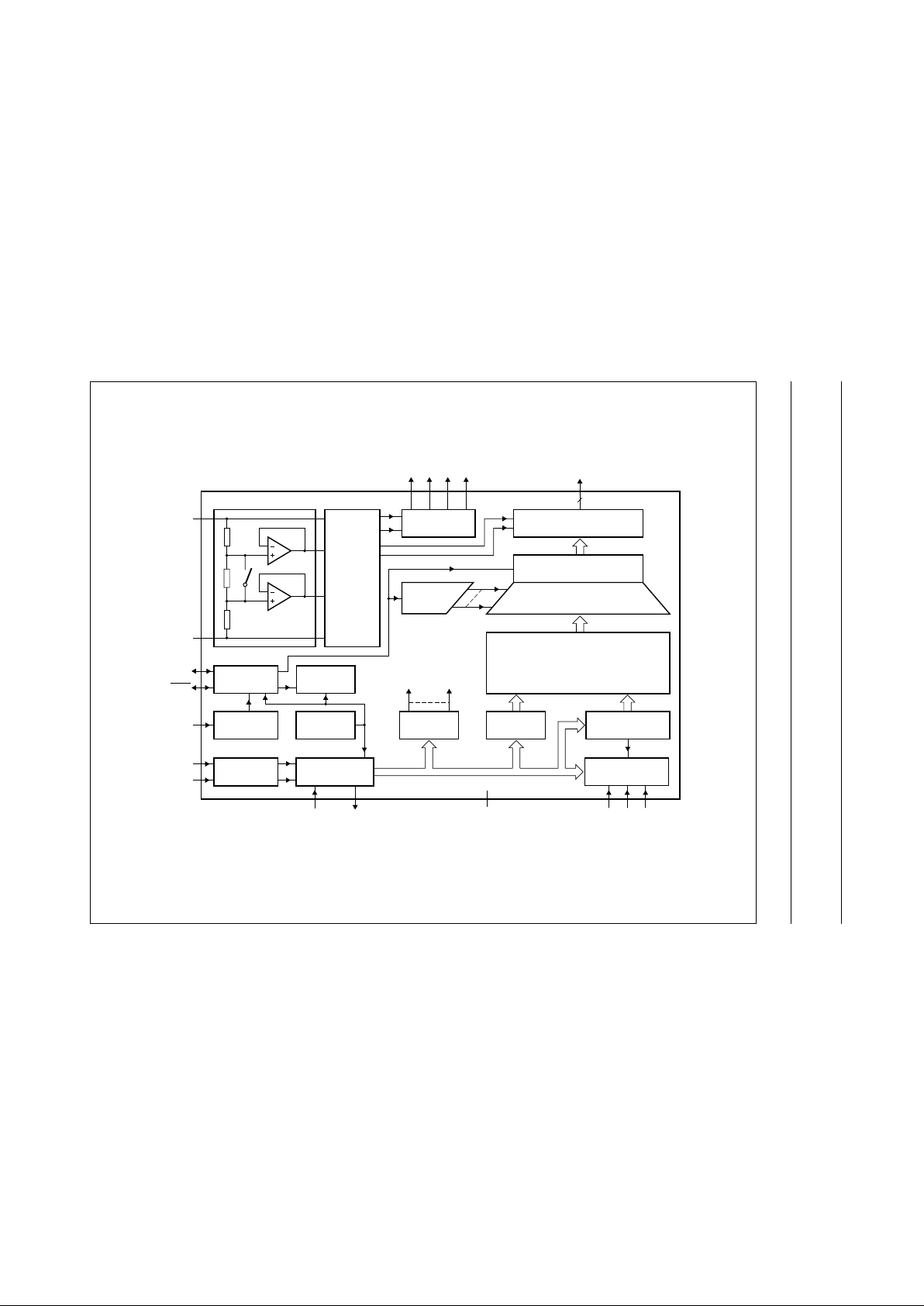
4 BLOCK DIAGRAM
Fig.1 Block diagram.
handbook, full pagewidth
MGL743
LCD
VOLTAGE
SELECTOR
CLOCK SELECT
AND TIMING
BLINKER
TIMEBASE
OSCILLATOR
INPUT
FILTERS
I
2
C-BUS
CONTROLLER
POWER-ON
RESET
CLK
SYNC
OSC
SCL
SDA
SA0
BACKPLANE
OUTPUTS
DISPLAY
CONTROL
BP0 BP1 BP2 BP3
DISPLAY SEGMENT OUTPUTS
DISPLAY REGISTER
OUTPUT BANK SELECT
AND BLINK CONTROL
80
S0 to S79
SDAACK V
DD
A0 A1 A2
PCF8533
LCD BIAS
GENERATOR
V
SS
V
LCD
COMMAND
DECODE
WRITE DATA
CONTROL
DISPLAY
RAM
DATA POINTER AND
AUTO INCREMENT
SUBADDRESS
COUNTER
Page 5
1999 Jul 30 5
Philips Semiconductors Product specification
Universal LCD driver for low multiplex rates PCF8533
5 PINNING
Note
1. For most applications SDA and SDAACK will be shorted together; see Chapter 7.
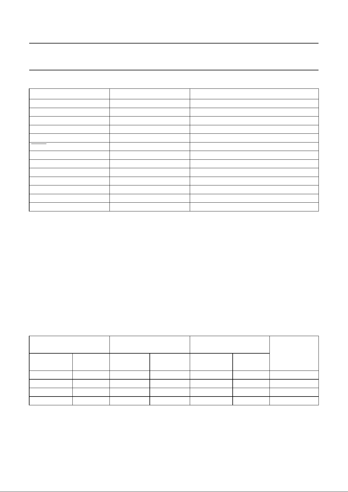
6 FUNCTIONAL DESCRIPTION
The PCF8533 is a versatile peripheral device designed to interface any microprocessor/microcontroller to a wide variety
of LCDs. It can directly drive any static or multiplexed LCD containing up to four backplanes and up to 80 segments.
The display configurations possible with the PCF8533 depend on the number of active backplane outputs required; a
selection of display configurations is given in Table 1.
All of the display configurations given in Table 1 can be implemented in the typical system shown in Fig.2.
The host microprocessor/microcontroller maintains the 2-line I
2
C-bus communication channel with the PCF8533.
The internal oscillator is selected by connecting pad OSC to VSS. The appropriate biasing voltages for the multiplexed
LCD waveforms are generated internally. The only other connections required to complete the system are to the power
supplies (VDD, VSSand V
LCD
) and the LCD panel selected for the application.
Table 1 Selection of display configurations
SYMBOL PAD DESCRIPTION
SDAACK 1 I2C-bus acknowledge output; note 1
SDA 2 and 3 I
2
C-bus serial data input; note 1
SCL 4 and 5 I
2
C-bus serial clock input
CLK 6 external clock input/output
V
DD
7 supply voltage
SYNC 8 cascade synchronization input/output
OSC 9 internal oscillator enable input
A0, A1 and A2 10, 11 and 12 subaddress inputs
SA0 13 I
2
C-bus slave address input; bit 0
V
SS
14 logic ground
V
LCD
15 LCD supply voltage
BP0, BP1, BP2 and BP3 17, 99, 16 and 98 LCD backplane outputs
S0 to S79 18 to 97 LCD segment outputs
NUMBER OF 7-SEGMENTS NUMERIC
14-SEGMENTS
ALPHANUMERIC
DOT MATRIX
BACKPLANES SEGMENTS DIGITS
INDICATOR
SYMBOLS
CHARACTERS
INDICATOR
SYMBOLS
4 320 40 40 20 40 320 dots (4 × 80)
3 240 30 30 16 16 240 dots (3 × 80)
2 160 20 20 10 20 160 dots (2 × 80)
1 80 10 10 5 10 80 dots (1 × 80)
Page 6
1999 Jul 30 6
Philips Semiconductors Product specification
Universal LCD driver for low multiplex rates PCF8533
Fig.2 Typical system configuration.
handbook, full pagewidth
HOST
MICRO-
PROCESSOR/
MICRO-
CONTROLLER
R
t
r
2C
B
SDA
SDAACK
SCL
OSC
80 segment drives
4 backplanes
LCD PANEL
(up to 320
elements)
PCF8533
A0 A1 A2 SA0
V
DD
V
SS
V
SS
V
DD
V
LCD
MGL744
Page 7
1999 Jul 30 7
Philips Semiconductors Product specification
Universal LCD driver for low multiplex rates PCF8533
6.1 Power-on reset
At Power-on the PCF8533 resets to a starting condition as
follows:
1. All backplane outputs are set to V
LCD
.
2. All segment outputs are set to V
LCD
.
3. Thedrivemode ‘1 : 4 multiplex with1⁄3bias’ is selected.
4. Blinking is switched off.
5. Input and output bank selectors are reset (as defined
in Table 5).
6. The I2C-bus interface is initialized.
7. The data pointer and the subaddress counter are
cleared.
8. Display disabled.
Data transfers on the I2C-bus should be avoided for 1 ms
following Power-on to allow completion of the reset action.
6.2 LCD bias generator
Fractional LCD biasing voltages are obtained from an
internal voltage divider of the three series resistors
connectedbetween V
LCD
andVSS.The centre resistor can
be switched out of the circuit to provide a1⁄2bias voltage
level for the 1 : 2 multiplex configuration.
6.3 LCD voltage selector
The LCD voltage selector co-ordinates the multiplexing of
the LCD in accordance with the selected LCD drive
configuration. The operation of the voltage selector is
controlled by MODE SET commands from the command
decoder.
The biasing configurations that apply to the preferred
modes of operation, together with the biasing
characteristics as functions of VOP and the resulting
discrimination ratios (D), are given in Table 2.
ApracticalvalueforVOPisdeterminedbyequatingV
off(rms)
with a defined LCD threshold voltage (Vth), typically when
the LCD exhibits approximately 10% contrast. In the static
drive mode a suitable choice is VOP>3Vth.
Multiplex drive ratios of 1 : 3 and 1 : 4 with
1
⁄2bias are
possible but the discrimination and hence the contrast
ratios are smaller ( = 1.732 for 1 : 3 multiplex or
= 1.528 for 1 : 4 multiplex).
The advantage of these modes is a reduction of the LCD
full-scale voltage V
OP
as follows:
• 1 : 3 multiplex (
1
⁄2bias):
• 1 : 4 multiplex (
1
⁄2bias):
These compare with V
OP
=3V
off(rms)
when1⁄3bias is used.
Note: VOP=V
LCD
.
3
21
3
----------
V
OP
6V
off(rms)
× 2.449V
off(rms)
==
V
OP
43×()
3
--------------------- -
2.309V
off(rms)
==
Table 2 Preferred LCD drive modes: summary of characteristics
LCD DRIVE MODE
NUMBER OF
LCD BIAS
CONFIGURATION
BACKPLANES LEVELS
static 1 2 static 0 1 ∞
1:2 2 3
1
⁄
2
0.354 0.791 2.236
1:2 2 4
1
⁄
3
0.333 0.745 2.236
1:3 3 4
1
⁄
3
0.333 0.638 1.915
1:4 4 4
1
⁄
3
0.333 0.577 1.732
V
off(rms)
V
OP
-------------------
V
on(rms)
V
OP
-------------------
D
V
on(rms)
V
off(rms)
-------------------
=
Page 8
1999 Jul 30 8
Philips Semiconductors Product specification
Universal LCD driver for low multiplex rates PCF8533
6.4 LCD drive mode waveforms
6.4.1 STATIC DRIVE MODE
The static LCD drive mode is used when a single backplane is provided in the LCD. Backplane and segment drive
waveforms for this mode are shown in Fig.3.
Fig.3 Static drive mode waveforms.
V
state1
(t)=Vsn(t) − V
BP0
(t).
V
on(rms)=VLCD
.
V
state2
(t)=V
sn +1
(t) − V
BP0
(t).
V
off(rms)
=0V.
handbook, full pagewidth
MGL745
V
SS
V
LCD
V
SS
V
LCD
V
SS
V
LCD
V
LCD
−V
LCD
−V
LCD
V
LCD
state 1 0 V
BP0
S
n
Sn + 1
state 2 0 V
(a) Waveforms at driver.
(b) Resultant waveforms
at LCD segment.
LCD segments
state 1
(on)
state 2
(off)
T
frame
Page 9

1999 Jul 30 9
Philips Semiconductors Product specification
Universal LCD driver for low multiplex rates PCF8533
6.4.2 1 : 2 MULTIPLEX DRIVE MODE
When two backplanes are provided in the LCD, the 1 : 2 multiplex mode applies. The PCF8533 allows the use of1⁄2bias
or1⁄3bias in this mode as shown in Figs 4 and 5.
Fig.4 Waveforms for the 1 : 2 multiplex drive mode with1⁄2bias.
V
state1
(t)=Vsn(t) − V
BP0
(t).
V
on(rms)
= 0.791V
LCD
.
V
state2
(t)=Vsn(t) − V
BP1
(t).
V
off(rms)
= 0.354V
LCD
.
handbook, full pagewidth
MGL746
state 1
BP0
(a) Waveforms at driver.
(b) Resultant waveforms
at LCD segment.
LCD segments
state 2
BP1
state 2
state 1
V
SS
V
LCD
V
LCD
/2
V
SS
V
SS
V
LCD
V
LCD
V
SS
V
LCD
V
LCD
V
LCD
0 V
0 V
V
LCD
/2
V
LCD
/2
V
LCD
/2
−V
LCD
−V
LCD
−V
LCD
/2
−V
LCD
/2
S
n
Sn + 1
T
frame
Page 10

1999 Jul 30 10
Philips Semiconductors Product specification
Universal LCD driver for low multiplex rates PCF8533
Fig.5 Waveforms for the 1 : 2 multiplex drive mode with1⁄3bias.
V
state1
(t)=Vsn(t) − V
BP0
(t).
V
on(rms)
= 0.745V
LCD
.
V
state2
(t)=Vsn(t) − V
BP1
(t).
V
off(rms)
= 0.333V
LCD
.
handbook, full pagewidth
MGL747
state 1
BP0
(a) Waveforms at driver.
(b) Resultant waveforms
at LCD segment.
LCD segments
state 2
BP1
state 1
state 2
V
SS
V
LCD
2V
LCD
/3
V
LCD
/3
V
SS
V
LCD
2V
LCD
/3
V
LCD
/3
V
SS
V
LCD
2V
LCD
/3
V
LCD
/3
0 V
V
LCD
2V
LCD
/3
−2V
LCD
/3
V
LCD
/3
−V
LCD
/3
−V
LCD
0 V
V
LCD
2V
LCD
/3
−2V
LCD
/3
V
LCD
/3
−V
LCD
/3
−V
LCD
S
n
Sn + 1
T
frame
V
SS
V
LCD
2V
LCD
/3
V
LCD
/3
6.4.3 1 : 3 MULTIPLEX DRIVE MODE
When three backplanes are provided in the LCD, the 1 : 3 multiplex drive mode applies, as shown in Fig.6.
Page 11

1999 Jul 30 11
Philips Semiconductors Product specification
Universal LCD driver for low multiplex rates PCF8533
Fig.6 Waveforms for the 1 : 3 multiplex drive mode.
V
state1
(t)=Vsn(t) − V
BP0
(t).
V
on(rms)
= 0.638V
LCD
.
V
state2
(t)=Vsn(t) − V
BP1
(t).
V
off(rms)
= 0.333V
LCD
.
handbook, full pagewidth
MGL748
state 1
BP0
(b) Resultant waveforms
at LCD segment.
LCD segments
state 2
BP1
state 1
state 2
(a) Waveforms at driver.
BP2
S
n
Sn + 1
Sn + 2
T
frame
V
SS
V
LCD
2V
LCD
/3
V
LCD
/3
V
SS
V
LCD
2V
LCD
/3
V
LCD
/3
V
SS
V
LCD
2V
LCD
/3
V
LCD
/3
V
SS
V
LCD
2V
LCD
/3
V
LCD
/3
V
SS
V
LCD
2V
LCD
/3
V
LCD
/3
0 V
V
LCD
2V
LCD
/3
−2V
LCD
/3
V
LCD
/3
−V
LCD
/3
−V
LCD
0 V
V
LCD
2V
LCD
/3
−2V
LCD
/3
V
LCD
/3
−V
LCD
/3
−V
LCD
V
SS
V
LCD
2V
LCD
/3
V
LCD
/3
6.4.4 1 : 4 MULTIPLEX DRIVE MODE
When four backplanes are provided in the LCD, the 1 : 4 multiplex drive mode applies, as shown in Fig.7.
Page 12

1999 Jul 30 12
Philips Semiconductors Product specification
Universal LCD driver for low multiplex rates PCF8533
handbook, full pagewidth
MGL749
state 1
BP0
(b) Resultant waveforms
at LCD segment.
LCD segments
state 2
BP1
state 1
state 2
BP2
(a) Waveforms at driver.
BP3
S
n
Sn + 1
Sn + 2
Sn + 3
T
frame
V
SS
V
LCD
2V
LCD
/3
V
LCD
/3
V
SS
V
LCD
2V
LCD
/3
V
LCD
/3
V
SS
V
LCD
2V
LCD
/3
V
LCD
/3
V
SS
V
LCD
2V
LCD
/3
V
LCD
/3
V
SS
V
LCD
2V
LCD
/3
V
LCD
/3
V
SS
V
LCD
2V
LCD
/3
V
LCD
/3
V
SS
V
LCD
2V
LCD
/3
V
LCD
/3
0 V
V
LCD
2V
LCD
/3
−2V
LCD
/3
V
LCD
/3
−V
LCD
/3
−V
LCD
0 V
V
LCD
2V
LCD
/3
−2V
LCD
/3
V
LCD
/3
−V
LCD
/3
−V
LCD
V
SS
V
LCD
2V
LCD
/3
V
LCD
/3
Fig.7 Waveforms for the 1 : 4 multiplex drive mode.
V
state1
(t)=Vsn(t) − V
BP0
(t): V
on(rms)
= 0.577V
LCD
.
V
state2
(t)=Vsn(t) − V
BP1
(t): V
off(rms)
= 0.333V
LCD
.
Page 13

1999 Jul 30 13
Philips Semiconductors Product specification
Universal LCD driver for low multiplex rates PCF8533
6.5 Oscillator
6.5.1 INTERNAL CLOCK
The internal logic and the LCD drive signals of the
PCF8533 are timed either by the built-in oscillator or from
an external clock. When the internal oscillator is used, pad
OSC should be connected to VSS. In this event, the output
from pad CLK provides the clock signal for cascaded
PCF8533s in the system. After power-up, SDA must be
HIGH to guarantee that the clock starts.
6.5.2 EXTERNAL CLOCK
The condition for external clock is made by tying pad OSC
to VDD; pad CLK then becomes the external clock input.
The clock frequency (f
CLK
) determines the LCD frame
frequency.
A clock signal must always be supplied to the device;
removing the clock may freeze the LCD in a DC state.
6.6 Timing
ThetimingofthePCF8533organizestheinternaldataflow
of the device. This includes the transfer of display data
from the display RAM to the display segment outputs.
In cascaded applications, the synchronization signal
(SYNC) maintains the correct timing relationship between
the PCF8533s in the system. The timing also generates
the LCD frame frequency which it derives as an integer
division of the clock frequency (see Table 3). The frame
frequency is a fixed division of the internal clock or of the
frequency applied to pad CLK when an external clock is
used.
6.7 Display register
The display latch holds the display data while the
corresponding multiplex signals are generated. There is a
one-to-one relationship between the data in the display
latch, the LCD segment outputs and one column of the
display RAM.
6.8 Segment outputs
The LCD drive section includes 80 segment outputs
(S0 to S79) which should be connected directly to the
LCD. The segment output signals are generated in
accordance with the multiplexed backplane signals and
with data resident in the display latch. When less than
80 segment outputs are required the unused segment
outputs should be left open-circuit.
6.9 Backplane outputs
The LCD drive section includes four backplane outputs
BP0 to BP3 which should be connected directly to the
LCD. The backplane output signals are generated in
accordance with the selected LCD drive mode.If less than
four backplane outputs are required the unused outputs
can be left open-circuit. In the 1 : 3 multiplex drive mode
BP3 carries the same signal as BP1, therefore these two
adjacent outputs can be tied together to give enhanced
drive capabilities. In the 1 : 2 multiplex drive mode
BP0 and BP2, BP1 and BP3 respectively carry the same
signals and may also be paired to increase the drive
capabilities. In the static drive mode the same signal is
carried by all four backplane outputs and they can be
connected in parallel for very high drive requirements.
6.10 Display RAM
The display RAM is a static 80 × 4-bit RAM which stores
LCD data. A logic 1 in the RAM bit map indicates the
on-state of the corresponding LCD segment; similarly, a
logic 0 indicates the off-state. There is a one-to-one
correspondence between the RAM addresses and the
segmentoutputs,andbetweentheindividualbitsofaRAM
word and the backplane outputs. The first RAM column
corresponds to the 80 segments operated with respect to
backplane BP0 (see Fig.8). In multiplexed LCD
applications the segment data of the second, third and
fourth column of the display RAM are time-multiplexed
with BP1, BP2 and BP3 respectively.
Page 14

1999 Jul 30 14
Philips Semiconductors Product specification
Universal LCD driver for low multiplex rates PCF8533
When display data is transmitted to the PCF8533 the
display bytes received are stored in the display RAM in
accordancewith the selected LCD drivemode. The data is
stored as it arrives and does not wait for the acknowledge
cycle as with the commands. Depending on the current
mux mode data is stored singularly, in pairs, triplets or
quadruplets.e.g.in1 : 2muxmodetheRAMdataisstored
every second bit. To illustrate the filling order, an example
of a 7-segment numeric display showing all drive modes is
given in Fig.9; the RAM filling organization depicted
applies equally to other LCD types. With reference to
Fig.9, in the static drive mode the eight transmitted data
bits are placed in bit 0 of eight successive display RAM
addresses. In the 1 : 2 multiplex drive mode the eight
transmitted data bits are placed in bits 0 and 1 of four
successive display RAM addresses.
In the 1 : 3 multiplex drive mode these bits are placed in
bits 0, 1 and 2 of three successive addresses, with bit 2 of
the third address left unchanged. This last bit may, if
necessary, be controlled by an additional transfer to this
address but care should be taken to avoid overriding
adjacent data because full bytes are always transmitted.
In the 1 : 4 multiplex drive mode the eight transmitted data
bits are placed in bits 0, 1, 2 and 3 of two successive
display RAM addresses.
Table 3 LCD frame frequencies
FRAME FREQUENCY
NOMINAL FRAME
FREQUENCY (Hz)
64
f
CLK
24
---------- -
Fig.8 Display RAM bit map showing direct relationship between display RAM addresses and segment outputs,
and between bits in a RAM word and backplane outputs.
andbook, full pagewidth
0
0
1
2
3
1234 7576777879
display RAM addresses (rows) / segment outputs (S)
display RAM bits
(columns) /
backplane outputs
(BP)
MGL750
Page 15

1999 Jul 30 15
Philips Semiconductors Product specification
Universal LCD driver for low multiplex rates PCF8533
6.11 Data pointer
The addressing mechanism for the display RAM is
realized using the data pointer. This allows the loading of
an individual display data byte, or a series of display data
bytes, into any location of the display RAM. The sequence
commenceswith the initialization of thedata pointer by the
LOAD DATA POINTER command. Following this, an
arriving data byte is stored starting at the display RAM
address indicated by the data pointer thereby observing
the filling order shown in Fig.9. The data pointer is
automatically incremented in accordance with the chosen
LCD configuration. That is, after each byte is stored, the
contents of the data pointer are incremented by eight
(static drive mode), by four (1 : 2 multiplex drive mode), by
three (1 : 3 multiplex drive mode) or by two (1 : 4 multiplex
drive mode). If an I2C-bus data access is terminated early
thenthestateofthedatapointerwillbeunknown.Thedata
pointer should be re-written prior to further RAM accesses.
6.12 Subaddress counter
The storage of display data is conditioned by the contents
of the subaddress counter. Storage is allowed to take
place only when the contents of the subaddress counter
agree with the hardware subaddress applied to
A0, A1 and A2. The subaddress counter value is defined
by the DEVICE SELECT command. If the contents of the
subaddress counter and the hardware subaddress do not
agree then data storage is inhibited but the data pointer is
incremented as if data storage had taken place.
The subaddress counter is also incremented when the
data pointer overflows.
The storage arrangements described lead to extremely
efficient data loading in cascaded applications. When a
series of display bytes are sent to the display RAM,
automatic wrap-over to the next PCF8533 occurs when
the last RAM address is exceeded. Subaddressing across
device boundaries is successful even if the change to the
next device in the cascade occurs within a transmitted
character (such as during the 27th display data byte
transmitted in 1 : 3 multiplex mode).
The hardware subaddress should not be changed whilst
the device is being accessed on the I2C-bus interface.
6.13 Output bank selector
The output bank selector selects one of the four bits per
display RAM address for transfer to the display latch.
The actual bit selected depends on the particular LCD
drive mode in operation and on the instant in the multiplex
sequence.
In 1 : 4 multiplex, all RAM addresses of bit 0 are selected,
these are followed by the contents of bit 1, bit 2 and then
bit 3. Similarly in 1 : 3 multiplex, bits 0, 1 and 2 are
selected sequentially. In 1 : 2 multiplex, bits 0 and 1 are
selected and, in the static mode, bit 0 is selected.
The SYNC signal will reset these sequences to the
following starting points; bit 3 for 1 : 4 multiplex, bit 2 for
1 : 3 multiplex, bit 1 for 1 : 2 multiplex and bit 0 for static
mode.
The PCF8533 includes a RAM bank switching feature in
the static and 1 : 2 multiplex drive modes. In the static
drive mode, the BANK SELECT command may request
the contents of bit 2 to be selected for display instead of
the contents of bit 0. In the 1 : 2 drive mode, the contents
of bits 2 and 3 may be selected instead of bits 0 and 1.
This gives the provision for preparing display information
in an alternative bank and to be able to switch to it once it
is assembled.
6.14 Input bank selector
The input bank selector loads display data into the display
RAM in accordance with the selected LCD drive
configuration. Display data can be loaded in bit 2 in static
drive mode or in bits 2 and 3 in 1 : 2 drive mode by using
Page 16

1999 Jul 30 16
Philips Semiconductors Product specification
Universal LCD driver for low multiplex rates PCF8533
the BANK SELECT command. The input bank selector
functions independently to the output bank selector.
6.15 Blinker
The display blinking capabilities of the PCF8533 are very
versatile. The whole display can be blinked at frequencies
selectedbytheBLINKcommand.Theblinking frequencies
are integer multiples of the clock frequency. The ratios
between the clock and blinking frequencies depend on the
mode in which the device is operating, see Table 4.
An additional feature is for an arbitrary selection of LCD
segments to be blinked. This applies to the static and
1 : 2 LCD drive modes and can be implemented without
any communication overheads. By means of the output
bank selector, the displayed RAM banks are exchanged
with alternate RAM banks at the blinking frequency. This
mode can also be specified by the BLINK command.
In the 1 : 3 and 1 : 4 multiplex modes, where no alternate
RAM bank is available, groups of LCD segments can be
blinked by selectively changing the display RAM data at
fixed time intervals.
If the entire display is to be blinked at a frequency other than the nominal blinking frequency, this can be effectively
performed by resetting and setting the display enable bit E at the required rate using the MODE SET command.
Table 4 Blinking frequencies
BLINKING MODE
NORMAL OPERATING MODE
RATIO
NOMINAL BLINKING FREQUENCY
Off − blinking off
2Hz 2Hz
1Hz 1Hz
0.5 Hz 0.5 Hz
f
CLK
768
---------- -
f
CLK
1536
------------ -
f
CLK
3072
------------ -
Page 17

1999 Jul 30 17
Philips Semiconductors Product specification
Universal LCD driver for low multiplex rates PCF8533
This text is here in white to force landscape pages to be rotated correctly when browsing through the pdf in the Acrobat reader.This text is here in
_white to force landscape pages to be rotated correctly when browsing through the pdf intheAcrobatreader.This text is here inThis text is here in
white to forcelandscape pages to be rotated correctlywhen browsing through the pdf inthe Acrobat reader. white to forcelandscape pages to be ...
handbook, full pagewidth
MGL751
S
2
n
S
1
n
S
7
n
S
n
S
n
S
3
n
S
5
n
S
2
n
S
3
n
S
1
n
S
1
n
S
1
n
S
2
n
S
n
S
6
n
S
n
S
4
n
DP
DP
DP
DP
a
f
b
g
e
c
d
a
f
b
g
e
c
d
a
f
b
g
e
c
d
a
f
b
g
e
c
d
BP0
BP0
BP0
BP1
BP1
BP2
BP1
BP2
BP3
BP0
n
c
x
x
x
0
1
2
3
b
x
x
x
a
x
x
x
f
x
x
x
g
x
x
x
e
x
x
x
d
x
x
x
DP
x
x
x
n1
n2 n3 n4 n5 n6 n7
bit/
BP
n
a
b
x
x
0
1
2
3
f
g
x
x
e
c
x
x
d
DP
x
x
n1
n2 n3
bit/
BP
n
b
DP
c
x
0
1
2
3
a
d
g
x
f
e
x
x
n1
n2
bit/
BP
n
a
c
b
DP
0
1
2
3
f
e
g
d
n1
bit/
BP
cbaf gedDP
abf gecdDP
bDPcadgf e
acbDPf egd
MSB LSB
MSB LSB
MSB LSB
MSB LSB
drive mode
static
1 : 2
multiplex
1 : 3
multiplex
1 : 4
multiplex
LCD segments LCD backplanes display RAM filling order transmitted display byte
Fig.9 Relationships between LCD layout, drive mode, display RAM filling order and display data transmitted over the I2C-bus.
X =data bit unchanged.
Page 18

1999 Jul 30 18
Philips Semiconductors Product specification
Universal LCD driver for low multiplex rates PCF8533
7 CHARACTERISTICS OF THE I2C-BUS
The I2C-bus is for bidirectional, two-line communication
between different ICs or modules. The two lines are a
Serial Data line (SDA) and a Serial Clock Line (SCL). Both
lines must be connected to a positive supply via a pull-up
resistor when connected to the output stages of a device.
Data transfer may be initiated only when the bus is not
busy.
Byconnecting SDAACK to SDA on the PCF8533, the SDA
line becomes fully I2C-bus compatible. Having the
acknowledge output separated from the serial data line is
advantageous in Chip-On-Glass (COG) applications.
In COG applications where the track resistance from the
SDAACK pad to the system SDA line can be significant, a
potential divider is generated by the bus pull-up resistor
and the Indium Tin Oxide (ITO) track resistance. It is
possible that during the acknowledge cycle the PCF8533
will not be able to create a valid logic 0 level. By splitting
the SDA input from the output the device could be used in
a mode that ignores the acknowledge bit. In COG
applications where the acknowledge cycle is required, it is
necessary to minimize the track resistance from the
SDAACK pad to the system SDA line to guarantee a valid
low level.
The following definition assumes SDA and SDAACK are
connected and refers to the pair as SDA.
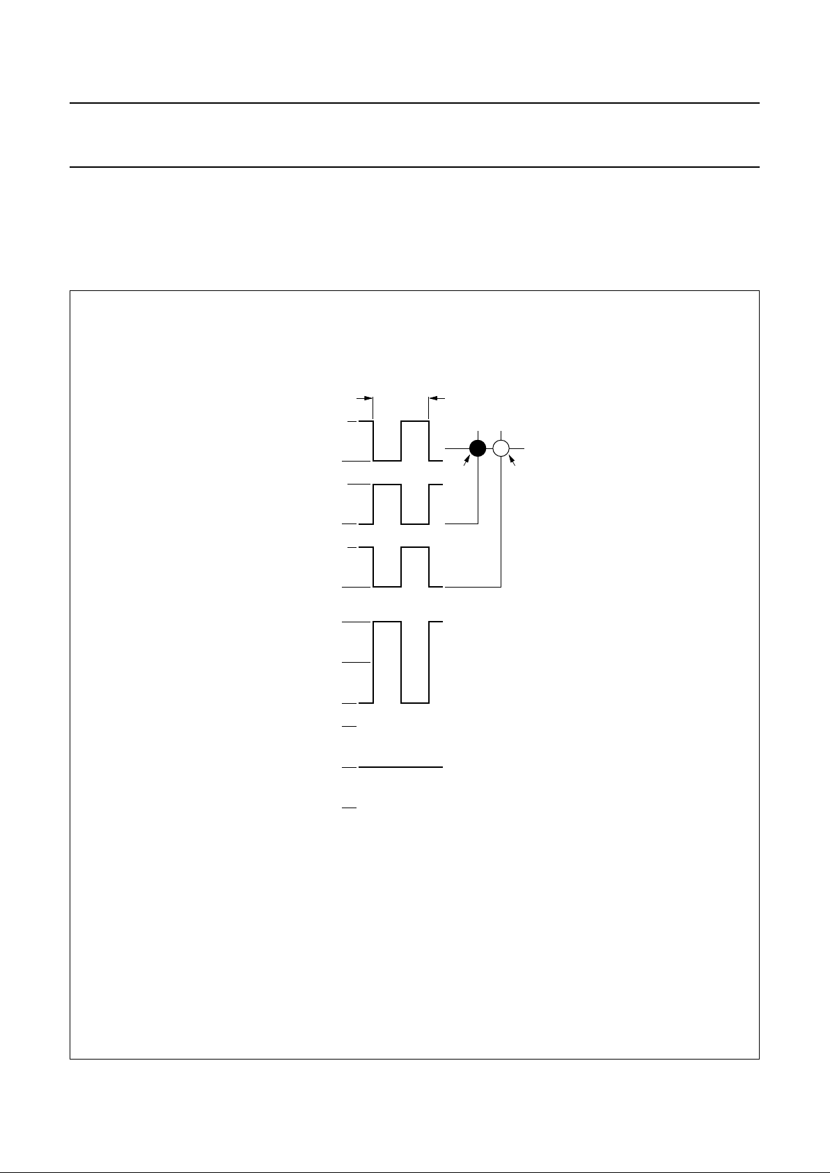
7.1 Bit transfer
One data bit is transferred during each clock pulse.
The data on the SDA line must remain stable during the
HIGH period of the clock pulse as changes in the data line
at this time will be interpreted as a control signal. Bit
transfer is illustrated in Fig.10.
7.2 START and STOP conditions
Bothdataand clock lines remain HIGH when the bus is not
busy. A HIGH-to-LOW transition of the data line, while the
clock is HIGH is defined as the START condition (S).
A LOW-to-HIGH transition of the data line while the clock
is HIGH is defined as the STOP condition (P). The START
and STOP conditions are illustrated in Fig.11.
7.3 System configuration
A device generating a message is a ‘transmitter’, a device
receiving a message is the ‘receiver’. The device that
controlsthemessageisthe‘master’andthedeviceswhich
are controlled by the master are the ‘slaves’. The system
configuration is illustrated in Fig.12.
7.4 Acknowledge
The number of data bytestransferred between the START
and STOP conditions from transmitter to receiver is
unlimited. Each byte of eight bits is followed by an
acknowledge bit. The acknowledge bit is a HIGH level
signal put on the bus by the transmitter during which time
the master generates an extra acknowledge related clock
pulse. A slave receiver which is addressed must generate
an acknowledge after the reception of each byte. Also a
master receiver must generate an acknowledge after the
reception of each byte that has been clocked out of the
slave transmitter. The device that acknowledges must
pull-down the SDA line during the acknowledge clock
pulse, so that the SDA line is stable LOW during the HIGH
period of the acknowledge related clock pulse (set-up and
hold times must be taken into consideration). A master
receiver must signal an end of data to the transmitter by
not generating an acknowledge on the last byte that has
been clocked out of the slave. In this event the transmitter
must leave the data line HIGH to enable the master to
generate a STOP condition. Acknowledgement on the
I
2
C-bus is illustrated in Fig.13.
7.5 PCF8533 I
2
C-bus controller
The PCF8533 acts as an I2C-bus slave receiver. It does
not initiate I2C-bus transfers or transmit data to an I2C-bus
master receiver. The only data output from the PCF8533
are the acknowledge signals of the selected devices.
Device selection depends on the I2C-bus slave address,
on the transferred command data and on the hardware
subaddress.
In single device application, the hardware subaddress
inputs A0, A1 and A2 are normally tied to VSS which
defines the hardware subaddress 0. In multiple device
applications A0, A1 and A2 are tied to VSSor VDD in
accordance with a binary coding scheme such that no two
devices with a common I2C-bus slave address have the
same hardware subaddress.
7.6 Input filters
To enhance noise immunity in electrically adverse
environments, RC low-pass filters are provided on the
SDA and SCL lines.
Page 19

1999 Jul 30 19
Philips Semiconductors Product specification
Universal LCD driver for low multiplex rates PCF8533
7.7 I2C-bus protocol
Two I2C-bus slave addresses (01110000 and 01110010)
are reserved for the PCF8533. The least significant bit of
the slave address that a PCF8533 will respond to is
defined by the level tied at its input SA0. The PCF8533 is
a write only device and will not respond to a read access.
Therefore, two types of PCF8533 can be distinguished on
the same I2C-bus which allows:
1. Upto16 PCF8533s on the same I2C-busforverylarge
LCD applications
2. The use of two types of LCD multiplex on the same
I2C-bus.
The I2C-bus protocol is shown in Fig.14. The sequence is
initiated with a START condition (S) from the I2C-bus
master which is followed by one of the two PCF8533 slave
addressesavailable.AllPCF8533swiththecorresponding
SA0levelacknowledgeinparalleltotheslaveaddress,but
all PCF8533s with the alternative SA0 level ignore the
whole I2C-bus transfer.
After acknowledgement, a control byte follows which
defines if the next byte is RAM or command information.
The control byte also defines if the next following byte is a
control byte or further RAM/command data.
In this way it is possible to configure the device then fill the
display RAM with little overhead.
The command bytes and control bytes are also
acknowledged by all addressed PCF8533s connected to
the bus.
The display bytes are stored in the display RAM at the
address specified by the data pointer and the subaddress
counter. Both data pointer and subaddress counter are
automatically updated and the data is directed to the
intended PCF8533 device.
The acknowledgement after each byte is made only bythe
(A0, A1 and A2) addressed PCF8533. After the last
display byte, the I
2
C-bus master issues a STOP
condition (P). Alternatively a START may be issued to
RESTART an I2C-bus access.
7.8 Command decoder
The command decoder identifies command bytes that
arrive on the I2C-bus. The five commands available to the
PCF8533 are defined in Table 5.
Fig.10 Bit transfer.
MBA607
data line
stable;
data valid
change
of data
allowed
SDA
SCL
Page 20

1999 Jul 30 20
Philips Semiconductors Product specification
Universal LCD driver for low multiplex rates PCF8533
Fig.11 Definition of START and STOP conditions.
handbook, full pagewidth
MBC622
SDA
SCL
P
STOP condition
SDA
SCL
S
START condition
Fig.12 System configuration.
MGA807
SDA
SCL
MASTER
TRANSMITTER/
RECEIVER
MASTER
TRANSMITTER
SLAVE
TRANSMITTER/
RECEIVER
SLAVE
RECEIVER
MASTER
TRANSMITTER/
RECEIVER
Fig.13 Acknowledgement on the I2C-bus.
handbook, full pagewidth
MBC602
S
START
condition
9821
clock pulse for
acknowledgement
not acknowledge
acknowledge
DATA OUTPUT
BY TRANSMITTER
DATA OUTPUT
BY RECEIVER
SCL FROM
MASTER
Page 21

1999 Jul 30 21
Philips Semiconductors Product specification
Universal LCD driver for low multiplex rates PCF8533
This text is here in white to force landscape pages to be rotated correctly when browsing through the pdf in the Acrobat reader.This text is here in
_white to force landscape pages to be rotated correctly when browsing through the pdf intheAcrobatreader.This text is here inThis text is here in
white to forcelandscape pages to be rotated correctlywhen browsing through the pdf inthe Acrobat reader. white to forcelandscape pages to be ...
EXAMPLES
a) transmit two bytes of RAM data
MGL752
S
A
0
S 01110 00
control byte
slave address
RAM/command byte
RAM DATA
M
S
B
L
S
B
A
A
P
R/W = 0
S
A
0
S 01110 0 010
A
A
A
P
RAM DATA
A
b) transmit two command bytes
COMMAND
S
A
0
S 01110 0 100
A
A
A
P
COMMAND
A
A
c) transmit one command byte and two RAM bytes
COMMAND
S
A
0
S 01110 0 10
00
010
A
A
A
P
RAM DATA
A
RAM DATA
A
A
CoRS
Fig.14 I2C-bus protocol.
Fig.15 Format of control byte.
Co =0; last control byte.
Co =1; control bytes continue.
RS =0; data is a command byte
RS =1; data is a display byte
MGL753
UNUSED
Co RS
MSB LSB
Page 22

1999 Jul 30 22
Philips Semiconductors Product specification
Universal LCD driver for low multiplex rates PCF8533
Table 5 Definition of PCF8533 commands
Table 6 Mode set option 1
Table 7 Mode set option 2
Table 8 Mode set option 3
COMMAND OPCODE OPTIONS DESCRIPTION
MODE SET 1 1 0 0 E B M1 M0 Table 6 defines LCD drive mode
Table 7 defines LCD bias configuration
Table 8 defines display status; the possibility to
disable the display allows implementation of
blinking under external control
LOADDATA
POINTER
0 P6 P5 P4 P3 P2 P1 P0 Table 9 seven bits of immediate data, bits P6 to P0,
are transferred to the data pointer to define
one of eighty display RAM addresses
DEVICE
SELECT
1 1 1 0 0 A2 A1 A0 Table 10 three bits of immediate data, bits A0 to A3,
are transferred to the subaddress counter to
define one of eight hardware subaddresses
BANK
SELECT
1 1 1 1 1 0 I O Table 11 defines input bank selection (storage of
arriving display data)
Table 12 defines output bank selection (retrieval of
LCD display data); the BANK SELECT
command has no effect in 1 : 3 and 1 : 4
multiplex drive modes
BLINK 1 1 1 1 0 A BF1BF0Table 13 defines the blinking frequency
Table 14 selects the blinking mode; normal operation
with frequency set by BF1, BF0 or blinking by
alternation of display RAM banks. Alternation
blinking does not apply in 1 : 3 and 1 : 4
multiplex drive modes
LCD DRIVE MODE BITS
DRIVE MODE BACKPLANE M1 M0
Static 1 BP 0 1
1 : 2 MUX (2 BP) 1 0
1 : 3 MUX (3 BP) 1 1
1 : 4 MUX (4 BP) 0 0
LCD BIAS BIT B
1
⁄3bias 0
1
⁄2bias 1
DISPLAY STATUS BIT E
Disabled (blank) 0
Enabled 1
Page 23

1999 Jul 30 23
Philips Semiconductors Product specification
Universal LCD driver for low multiplex rates PCF8533
Table 9 Load data pointer option 1
Table 10 Device select option 1
Table 11 Bank select option 1 (Input)
Table 12 Bank select option 2 (Output)
Table 13 Blink option 1
Table 14 Blink option 2
Note
1. Normal blinking is assumed when multiplex rates 1 : 3
or 1 : 4 are selected.
7.9 Display controller
The display controller executes the commands identified
by the command decoder. It contains the status registers
of the PCF8533 and co-ordinates their effects.
The controller is also responsible for loading display data
into the display RAM as required by the filling order.
7.10 Cascaded operation
In large display configurations, up to 16 PCF8533s can be
distinguished on the same I2C-bus by using the 3-bit
hardware subaddress (A0, A1 and A2) and the
programmable I2C-bus slave address (SA0). When
cascaded PCF8533s are synchronized they can share the
backplane signals from one of the devices in the cascade.
Such an arrangement is cost-effective in large LCD
applications since the backplane outputs of only one
device need to be through-plated to the backplane
electrodes of the display. The other PCF8533s of the
cascade contribute additional segment outputs but their
backplane outputs are left open-circuit (see Fig.16).
The SYNC line is provided to maintain the correct
synchronization between all cascaded PCF8533s. This
synchronization is guaranteed after the Power-on reset.
The only time that SYNC is likely to be needed is if
synchronization is accidentally lost (e.g. by noise in
adverse electrical environments, or by the definition of a
multiplex mode when PCF8533s with different SA0 levels
are cascaded). SYNC is organizedas an input/output pad;
the output selection being realized as an open-drain driver
with an internal pull-up resistor. A PCF8533 asserts the
SYNC line at the onset of its last active backplane signal
and monitors the SYNC line at all other times. Should
synchronization in the cascade be lost, it will be restored
by the first PCF8533 to assert SYNC. The timing
relationship between the backplane waveforms and the
SYNC signal for the various drive modes of the PCF8533
are shown in Fig.17.
The contact resistance between the SYNC pads of
cascaded devices must be controlled. If the resistance is
too high then the device will not be able to synchronize
properly. This is particularly applicable to COG
applications. Table 15 shows the limiting values for
contact resistance.
Table 15 SYNC contact resistance
DESCRIPTION BITS
7 bit binary value of
0to79
P6 P5 P4 P3 P2 P1 P0
DESCRIPTION BITS
3 bit binary value of 0 to 7 A2 A1 A0
STATIC 1 : 2 MUX BIT I
RAM bit 0 RAM bits 0 and 1 0
RAM bit 2 RAM bits 2 and 3 1
STATIC 1 : 2 MUX BIT O
RAM bit 0 RAM bits 0 and 1 0
RAM bit 2 RAM bits 2 and 3 1
BLINK FREQUENCY
BITS
BF1 BF0
Off 0 0
2Hz 0 1
1Hz 1 0
0.5 Hz 1 1
BLINK MODE BITA
Normal blinking
(1)
0
Alternation blinking 1
NUMBER OF DEVICES
MAXIMUM CONTACT
RESISTANCE
2 6000 Ω
3 to 5 2200 Ω
6 to 10 1200 Ω
11 to 16 700 Ω
Page 24

1999 Jul 30 24
Philips Semiconductors Product specification
Universal LCD driver for low multiplex rates PCF8533
Fig.16 Cascaded PCF8533 configuration.
handbook, full pagewidth
HOST
MICRO-
PROCESSOR/
MICRO-
CONTROLLER
SDA
SCL
CLK
OSC
SYNC
80 segment drives
4 backplanes
80 segment drives
LCD PANEL
(up to 5120
elements)
PCF8533
A0 A1 A2 SA0
V
SS
V
SS
V
SS
V
DD
V
DD
V
LCD
V
LCD
V
DDVLCD
MGL754
SDA
SDAACK
SDAACK
SCL
SYNC
CLK
OSC
BP0 to BP3
(open-circuit)
A0 A1 A2 SA0
PCF8533
BP0 to BP3
R
t
r
2C
B
Page 25

1999 Jul 30 25
Philips Semiconductors Product specification
Universal LCD driver for low multiplex rates PCF8533
Fig.17 Synchronization of the cascade for the various PCF8533 drive modes.
handbook, full pagewidth
T=
framefframe
1
BP0
SYNC
BP1
(1/2 bias)
SYNC
BP2
(a) static drive mode.
(b) 1 : 2 multiplex drive mode.
(c) 1 : 3 multiplex drive mode.
(d) 1 : 4 multiplex drive mode.
BP3
SYNC
SYNC
BP1
(1/3 bias)
MGL755
Page 26

1999 Jul 30 26
Philips Semiconductors Product specification
Universal LCD driver for low multiplex rates PCF8533
8 LIMITING VALUES
In accordance with the Absolute Maximum Rating System (IEC 134).
9 HANDLING
Inputs and outputs are protected against electrostatic discharge in normal handling. However, to be totally safe, it is
desirable to take normal precautions appropriate to handling MOS devices (see
“Handling MOS Devices”
).
SYMBOL PARAMETER MIN. MAX. UNIT
V
DD
supply voltage −0.5 +6.5 V
I
DD
supply current −50 +50 mA
V
LCD
LCD supply voltage VSS− 0.5 +7.5 V
I
LCD
LCD supply current −50 +50 mA
I
SS
negative supply current −50 +50 mA
V
I(n)
input voltage on pads SDA, SCL, CLK, SYNC, SA0, OSC
and A0 to A2
VSS− 0.5 VDD+ 0.5 V
V
O(n)
output voltage on pads S0 to S79 and BP0 to BP3 VSS− 0.5 V
LCD
+ 0.5 V
I
I
DC input current −10 +10 mA
I
O
DC output current −10 +10 mA
P
tot
total power dissipation − 400 mW
P/out power dissipation per output − 100 mW
T
stg
storage temperature −65 +150 °C
Page 27

1999 Jul 30 27
Philips Semiconductors Product specification
Universal LCD driver for low multiplex rates PCF8533
10 DC CHARACTERISTICS
VDD= 1.8 to 5.5 V; VSS=0V;V
LCD
= 2.5 to 6.5 V; T
amb
= −40 to +85 °C; unless otherwise specified.
Notes
1. LCD outputs are open-circuit; inputs at V
SS
or VDD; external clock with 50% duty factor; I2C-bus inactive.
2. Not tested; given by design.
3. Outputs measured one at a time.
SYMBOL PARAMETER CONDITIONS MIN. TYP. MAX. UNIT
Supplies
V
DD
supply voltage 1.8 − 5.5 V
V
LCD
LCD supply voltage 2.5 − 6.5 V
I
DD
supply current f
CLK
= 1536 Hz; note 1 − 820µA
I
LCD
LCD supply current f
CLK
= 1536 Hz; note 1 − 24 60 µA
Logic
V
IL
LOW-level input voltage V
SS
− 0.3V
DD
V
V
IH
HIGH-level input voltage 0.7V
DD
− V
DD
V
I
OL1
LOW-level output current on pads
CLK and SYNC
VOL= 0.4 V; VDD=5V 1 −−mA
I
OH1
HIGH-level output current pad CLK VOH= 4.6 V;
VDD=5V
−1 −−mA
I
OL2
LOW-level output current pad SDA VOL= 0.4 V; VDD=5V 3 −−mA
I
L1
leakage current on pads SA0,
A0 to A2, CLK, SDA and SCL
VI=VDD or V
SS
−1 − +1 µA
I
L2
leakage current pad OSC VI=V
DD
−1 − +1 µA
V
POR
Power-on reset voltage level 1.0 1.3 1.6 V
C
I
input capacitance note 2 −−7pF
LCD outputs
V
BP
DC voltage component on pads
BP0 to BP3
CBP=35nF −100 − +100 mV
V
S
DC voltage component on pads
S0 to S79
CS=5nF −100 − +100 mV
R
BP
output resistance at pads BP0 to BP3 V
LCD
= 5 V; note 3 − 1.5 10 kΩ
R
S
output resistance at pads S0 to S79 V
LCD
= 5 V; note 3 − 6.0 13.5 kΩ
Page 28

1999 Jul 30 28
Philips Semiconductors Product specification
Universal LCD driver for low multiplex rates PCF8533
11 AC CHARACTERISTICS
VDD= 1.8 to 5.5 V; VSS=0V; V
LCD
= 2.5 to 6.5 V; T
amb
= −40 to + 85 °C; unless otherwise specified.
Notes
1. Typical output duty cycle of 50%.
2. All timing values are valid within the operating supply voltage and ambient temperature range and are referenced to
V
IL
and VIH with an input voltage swing of VSSto VDD.
SYMBOL PARAMETER CONDITIONS MIN. TYP. MAX. UNIT
f
CLK
oscillator frequency at pad CLK VDD= 5 V; note 1 797 1536 3046 Hz
t
CLKH
input CLK HIGH time 130 −−µs
t
CLKL
input CLK LOW time 130 −−µs
t
d(p)SYNC
SYNC propagation delay time − 30 − ns
t
SYNCL
SYNC LOW time 1 −−µs
t
d(PLCD)
driver delays with test loads V
LCD
=5V −−30 µs
Timing characteristics: I
2
C-bus; note 2
f
SCL
SCL clock frequency −−400 kHz
t
BUF
bus free time between a STOP and START 1.3 −−µs
t
HD;STA
START condition hold time 0.6 −−µs
t
SU;STA
set-up time for a repeated START condition 0.6 −−µs
t
LOW
SCL LOW time 1.3 −−µs
t
HIGH
SCL HIGH time 0.6 −−µs
t
r
SCL and SDA rise time −−0.3 µs
t
f
SCL and SDA fall time −−0.3 µs
C
b
capacitive bus line load −−400 pF
t
SU;DAT
data set-up time 100 −−ns
t
HD;DAT
data hold time 0 −−ns
t
SU;STO
set-up time for STOP condition 0.6 −−µs
t
SW
tolerable spike width on bus −−50 ns
Fig.18 Test loads.
handbook, full pagewidth
MGS120
Ω3.3 k Ω1.5 k
0.5V
DD
V
DD
V
SS
SDA,
SCL
CLK
1 nF
BP0 to BP3, and
S0 to S79
(2%)(2%)
Ω6.8
V
DD
SYNC
(2%)
Page 29

1999 Jul 30 29
Philips Semiconductors Product specification
Universal LCD driver for low multiplex rates PCF8533
Fig.19 Driver timing waveforms.
handbook, full pagewidth
MGL761
0.7V
DD
0.3V
DD
0.7V
DD
0.3V
DD
1/ f
CLK
t
d(p)(SYNC)
t
d(p)(SYNC)
t
CLKH
t
CLKL
SYNC
CLK
0.5 V
0.5 V
t
PLCD
BP0 to BP3,
and S0 to S79
t
SYNCL
(VDD = 5 V)
Fig.20 I2C-bus timing waveforms.
book, full pagewidth
SDA
MGA728
SDA
SCL
t
SU;STA
t
SU;STO
t
HD;STA
t
BUF
t
LOW
t
HD;DAT
t
HIGH
t
r
t
f
t
SU;DAT
Page 30

1999 Jul 30 30
Philips Semiconductors Product specification
Universal LCD driver for low multiplex rates PCF8533
12 BONDING PAD LOCATIONS
Bonding pad locations (dimensions in µm)
All x and y coordinates are referenced to centre of chip
(see Fig.22).
SYMBOL PAD x y
SDAACK 1 −1079.20 −594.40
SDA 2 −839.20 −594.40
SDA 3 −759.20 −594.40
SCL 4 −599.20 −594.40
SCL 5 −519.20 −594.40
CLK 6 −414.80 −594.40
V
DD
7 −284.80 −594.40
SYNC 8 +4.20 −594.40
OSC 9 +119.20 −594.40
A0 10 +249.20 −594.40
A1 11 +379.20 −594.40
A2 12 +581.20 −594.40
SA0 13 +711.20 −594.40
V
SS
14 +841.20 −594.40
V
LCD
15 +1099.60 −594.40
BP2 16 +1277.60 −594.40
BP0 17 +1357.60 −594.40
S0 18 +1437.60 −594.40
S1 19 +1517.60 −594.40
S2 20 +1597.60 −594.40
S3 21 +1677.60 −594.40
S4 22 +1757.60 −594.40
S5 23 +1837.60 −594.40
S6 24 +1917.60 −594.40
S7 25 +1997.60 −594.40
S8 26 +2077.60 −594.40
S9 27 +2157.60 −594.40
S10 28 +2237.60 −594.40
S11 29 +2317.60 −594.40
S12 30 +2357.60 +594.40
S13 31 +2277.60 +594.40
S14 32 +2197.60 +594.40
S15 33 +2117.60 +594.40
S16 34 +2037.60 +594.40
S17 35 +1957.60 +594.40
S18 36 +1877.60 +594.40
S19 37 +1797.60 +594.40
S20 38 +1717.60 +594.40
S21 39 +1637.60 +594.40
S22 40 +1557.60 +594.40
S23 41 +1477.60 +594.40
S24 42 +1317.60 +594.40
S25 43 +1237.60 +594.40
S26 44 +1157.60 +594.40
S27 45 +1077.60 +594.40
S28 46 +997.60 +594.40
S29 47 +917.60 +594.40
S30 48 +837.60 +594.40
S31 49 +757.60 +594.40
S32 50 +677.60 +594.40
S33 51 +597.60 +594.40
S34 52 +437.60 +594.40
S35 53 +357.60 +594.40
S36 54 +277.60 +594.40
S37 55 +197.60 +594.40
S38 56 +117.60 +594.40
S39 57 +37.60 +594.40
S40 58 −42.40 +594.40
S41 59 −122.40 +594.40
S42 60 −202.40 +594.40
S43 61 −282.40 +594.40
S44 62 −362.40 +594.40
S45 63 −442.40 +594.40
S46 64 −602.40 +594.40
S47 65 −682.40 +594.40
S48 66 −762.40 +594.40
S49 67 −842.40 +594.40
S50 68 −922.40 +594.40
S51 69 −1002.40 +594.40
S52 70 −1082.40 +594.40
S53 71 −1162.40 +594.40
S54 72 −1242.40 +594.40
S55 73 −1322.40 +594.40
S56 74 −1402.40 +594.40
SYMBOL PAD x y
Page 31

1999 Jul 30 31
Philips Semiconductors Product specification
Universal LCD driver for low multiplex rates PCF8533
S57 75 −1562.40 +594.40
S58 76 −1642.40 +594.40
S59 77 −1722.40 +594.40
S60 78 −1802.40 +594.40
S61 79 −1882.40 +594.40
S62 80 −1962.40 +594.40
S63 81 −2042.40 +594.40
S64 82 −2122.40 +594.40
S65 83 −2202.40 +594.40
S66 84 −2282.40 +594.40
S67 85 −2362.40 +594.40
S68 86 −2322.40 −594.40
S69 87 −2242.40 −594.40
S70 88 −2162.40 −594.40
S71 89 −2082.40 −594.40
S72 90 −2002.40 −594.40
S73 91 −1922.40 −594.40
S74 92 −1842.40 −594.40
S75 93 −1762.40 −594.40
S76 94 −1682.40 −594.40
S77 95 −1602.40 −594.40
S78 96 −1522.40 −594.40
SYMBOL PAD x y
Note
1. The dummy pads are not tested.
S79 97 −1442.40 −594.40
BP3 98 −1362.40 −594.40
BP1 99 −1282.40 −594.40
Alignment marks
C1 − +2300.5 +55.0
C2 −−2320.2 +107.0
F −−2208.3 −165.4
Dummy pads (connected to segments shown; note
D1 (S11) +2469.70 −594.40
D2 (S11) +2549.70 −594.40
D3 (S12) +2517.60 +594.40
D4 (S12) +2437.60 +594.40
D5 (S67) −2442.30 +594.40
D6 (S67) −2522.30 +594.40
D7 (S68) −2554.40 −594.40
D8 (S68) −2474.40 −594.40
Chip corners (pre-sawing)
Bottom left −−2695.00 −750.00
Top right − +2695.00 +750.00
SYMBOL PAD x y
Fig.21 Alignment markers.
handbook, halfpage
REF
REF
REF
C2 C1
F
MGL756
Page 32

1999 Jul 30 32
Philips Semiconductors Product specification
Universal LCD driver for low multiplex rates PCF8533
This text is here in white to force landscape pages to be rotated correctly when browsing through the pdf in the Acrobat reader.This text is here in
_white to force landscape pages to be rotated correctly when browsing through the pdf intheAcrobatreader.This text is here inThis text is here in
white to forcelandscape pages to be rotated correctlywhen browsing through the pdf inthe Acrobat reader. white to forcelandscape pages to be ...
o
k, full pagewidth
MGL759
SDAACK
SDA
SA0
SCL
SYNC
CLK
OSC
A0A1A2
V
DD
V
SS
V
LCD
...
...
...
...
...
D3
S67D5D6
S68
S79
BP3
S0S1S2
S11
D1
D2
BP0
BP2
BP1
D8
D7
D4
S12
...
PC8533-2
C
2
C
1
F
0,0
x
y
Fig.22 Bonding pad locations.
The position of the bonding pads is not to scale.
Chip dimensions: approximately 5.40 ×1.51 mm.
Bump dimensions: 90× 50 × 17.5 µm.
Wafer thickness: 381 µm.
Page 33

1999 Jul 30 33
Philips Semiconductors Product specification
Universal LCD driver for low multiplex rates PCF8533
13 DEVICE PROTECTION
Fig.23 Device protection diagram.
handbook, full pagewidth
SA0
V
DD
V
DD
V
SS
V
SS
V
LCD
V
SS
SDA
MGL760
V
SS
SDAACK
V
SS
SCL
V
SS
CLK
V
DD
V
SS
OSC
V
DD
V
SS
SYNC
V
DD
V
SS
A0, A1 A2
V
DD
V
SS
BP0, BP1,
BP2, BP3
V
LCD
V
SS
S0 to S79
V
LCD
V
SS
Page 34

1999 Jul 30 34
Philips Semiconductors Product specification
Universal LCD driver for low multiplex rates PCF8533
14 TRAY INFORMATION
Fig.24 Tray details.
handbook, full pagewidth
MGL757
D
C
A
x
y
F
E
B
The dimensions are given in Table 16.
Table 16 Dimensions
Fig.25 Tray alignment.
The orientationof the ICina pocket isindicatedby the positionof the
IC type name on the die surface with respect to the chamfer on the
upper left corner of the tray. Refer to the bonding pad location
diagram for the orientating and position of the type name on the die
surface.
handbook, halfpage
MGL758
PC8533-2
DIM. DESCRIPTION VALUE
A pocket pitch, x direction 7.37 mm
B pocket pitch, y direction 3.68 mm
C pocket width, x direction 5.50 mm
D pocket width, y direction 1.60 mm
E tray width, x direction 50.8 mm
F tray width, y direction 50.8 mm
x no. pockets in x direction 6
y no. pockets in y direction 12
Page 35

1999 Jul 30 35
Philips Semiconductors Product specification
Universal LCD driver for low multiplex rates PCF8533
15 DEFINITIONS
16 LIFE SUPPORT APPLICATIONS
These products are not designed for use in life support appliances, devices, or systems where malfunction of these
products can reasonably be expected to result in personal injury. Philips customers using or selling these products for
use in such applications do so at their own risk and agree to fully indemnify Philips for any damages resulting from such
improper use or sale.
17 PURCHASE OF PHILIPS I
2
C COMPONENTS
18 BARE DIE DISCLAIMER
All die are tested and are guaranteed to comply with all data sheet limits up to the point of wafer sawing for a period of
ninety (90) days from the date of Philips' delivery. If there are data sheet limits not guaranteed, these will be separately
indicated in the data sheet. There is no post waffle pack testing performed on individual die. Although the most modern
processes are utilized for wafer sawing and die pick and place into waffle pack carriers, Philips Semiconductors has no
control of third party procedures in the handling, packing or assembly of the die. Accordingly, Philips Semiconductors
assumes no liability for device functionality or performance of the die or systems after handling, packing or assembly of
the die. It is the responsibility of the customer to test and qualify their application in which the die is used.
Data sheet status
Objective specification This data sheet contains target or goal specifications for product development.
Preliminary specification This data sheet contains preliminary data; supplementary data may be published later.
Product specification This data sheet contains final product specifications.
Limiting values
Limiting values given are in accordance with the Absolute Maximum Rating System (IEC 134). Stress above one or
more of the limiting values may cause permanent damage to the device. These are stress ratings only and operation
of the device at these or at any other conditions above those given in the Characteristics sections of the specification
is not implied. Exposure to limiting values for extended periods may affect device reliability.
Application information
Where application information is given, it is advisory and does not form part of the specification.
Purchase of Philips I
2
C components conveys a license under the Philips’ I2C patent to use the
components in the I2C system provided the system conforms to the I2C specification defined by
Philips. This specification can be ordered using the code 9398 393 40011.
Page 36

© Philips Electronics N.V.
SCA
All rights are reserved. Reproduction in whole or in part is prohibited without the prior written consent of the copyright owner.
The information presented in this document does not form part of any quotation or contract, is believed to be accurate and reliable and may be changed
without notice. No liability will be accepted by the publisher for any consequence of its use. Publication thereof does not convey nor imply any license
under patent- or other industrial or intellectual property rights.
Internet: http://www.semiconductors.philips.com
1999
67
Philips Semiconductors – a w orldwide compan y
For all other countries apply to: Philips Semiconductors,
International Marketing & Sales Communications, Building BE-p, P.O. Box 218,
5600 MD EINDHOVEN, The Netherlands, Fax. +31 40 27 24825
Argentina: see South America
Australia: 3 Figtree Drive, HOMEBUSH, NSW 2140,
Tel. +61 2 9704 8141, Fax. +61 2 9704 8139
Austria: Computerstr. 6, A-1101 WIEN, P.O. Box 213,
Tel. +43 1 60 101 1248, Fax. +43 1 60 101 1210
Belarus: Hotel Minsk Business Center, Bld. 3, r. 1211, Volodarski Str. 6,
220050 MINSK, Tel. +375 172 20 0733, Fax. +375 172 20 0773
Belgium: see The Netherlands
Brazil: see South America
Bulgaria: Philips Bulgaria Ltd., Energoproject, 15th floor,
51 James Bourchier Blvd., 1407 SOFIA,
Tel. +359 2 68 9211, Fax. +359 2 68 9102
Canada: PHILIPS SEMICONDUCTORS/COMPONENTS,
Tel. +1 800 234 7381, Fax. +1 800 943 0087
China/Hong Kong: 501 Hong Kong Industrial Technology Centre,
72 Tat Chee Avenue, Kowloon Tong, HONG KONG,
Tel. +852 2319 7888, Fax. +852 2319 7700
Colombia: see South America
Czech Republic: see Austria
Denmark: Sydhavnsgade 23, 1780 COPENHAGEN V,
Tel. +45 33 29 3333, Fax. +45 33 29 3905
Finland: Sinikalliontie 3, FIN-02630 ESPOO,
Tel. +358 9 615 800, Fax. +358 9 6158 0920
France: 51 Rue Carnot, BP317, 92156 SURESNES Cedex,
Tel. +33 1 4099 6161, Fax. +33 1 4099 6427
Germany: Hammerbrookstraße 69, D-20097 HAMBURG,
Tel. +49 40 2353 60, Fax. +49 40 2353 6300
Hungary: see Austria
India: Philips INDIA Ltd, Band Box Building, 2nd floor,
254-D, Dr. Annie Besant Road, Worli, MUMBAI 400 025,
Tel. +91 22 493 8541, Fax. +91 22 493 0966
Indonesia: PTPhilips DevelopmentCorporation,Semiconductors Division,
Gedung Philips, Jl. Buncit Raya Kav.99-100, JAKARTA 12510,
Tel. +62 21 794 0040 ext. 2501, Fax. +62 21 794 0080
Ireland: Newstead, Clonskeagh, DUBLIN 14,
Tel. +353 1 7640 000, Fax. +353 1 7640 200
Israel: RAPAC Electronics, 7 Kehilat Saloniki St, PO Box 18053,
TEL AVIV 61180, Tel. +972 3 645 0444, Fax. +972 3 649 1007
Italy: PHILIPS SEMICONDUCTORS,ViaCasati, 23 - 20052 MONZA (MI),
Tel. +39 039 203 6838, Fax +39 039 203 6800
Japan: Philips Bldg 13-37, Kohnan 2-chome, Minato-ku,
TOKYO 108-8507, Tel. +81 3 3740 5130, Fax. +81 3 3740 5057
Korea: Philips House, 260-199 Itaewon-dong, Yongsan-ku, SEOUL,
Tel. +82 2 709 1412, Fax. +82 2 709 1415
Malaysia: No. 76 Jalan Universiti, 46200 PETALING JAYA, SELANGOR,
Tel. +60 3 750 5214, Fax. +60 3 757 4880
Mexico: 5900 Gateway East, Suite 200, EL PASO, TEXAS 79905,
Tel. +9-5 800 234 7381, Fax +9-5 800 943 0087
Middle East: see Italy
Netherlands: Postbus 90050, 5600 PB EINDHOVEN, Bldg. VB,
Tel. +31 40 27 82785, Fax. +31 40 27 88399
New Zealand: 2 Wagener Place, C.P.O. Box 1041, AUCKLAND,
Tel. +64 9 849 4160, Fax. +64 9 849 7811
Norway: Box 1, Manglerud 0612, OSLO,
Tel. +47 22 74 8000, Fax. +47 22 74 8341
Pakistan: see Singapore
Philippines: Philips Semiconductors Philippines Inc.,
106 Valero St. Salcedo Village, P.O. Box 2108 MCC, MAKATI,
Metro MANILA, Tel. +63 2 816 6380, Fax. +63 2 817 3474
Poland: Ul. Lukiska 10, PL 04-123 WARSZAWA,
Tel. +48 22 612 2831, Fax. +48 22 612 2327
Portugal: see Spain
Romania: see Italy
Russia: Philips Russia, Ul. Usatcheva 35A, 119048 MOSCOW,
Tel. +7 095 755 6918, Fax. +7 095 755 6919
Singapore: Lorong 1, Toa Payoh, SINGAPORE 319762,
Tel. +65 350 2538, Fax. +65 251 6500
Slovakia: see Austria
Slovenia: see Italy
South Africa: S.A. PHILIPS Pty Ltd., 195-215 Main Road Martindale,
2092 JOHANNESBURG, P.O. Box 58088 Newville 2114,
Tel. +27 11 471 5401, Fax. +27 11 471 5398
South America: Al. Vicente Pinzon, 173, 6th floor,
04547-130 SÃO PAULO, SP, Brazil,
Tel. +55 11 821 2333, Fax. +55 11 821 2382
Spain: Balmes 22, 08007 BARCELONA,
Tel. +34 93 301 6312, Fax. +34 93 301 4107
Sweden: Kottbygatan 7, Akalla, S-16485 STOCKHOLM,
Tel. +46 8 5985 2000, Fax. +46 8 5985 2745
Switzerland: Allmendstrasse 140, CH-8027 ZÜRICH,
Tel. +41 1 488 2741 Fax. +41 1 488 3263
Taiwan: Philips Semiconductors, 6F, No. 96, Chien Kuo N. Rd., Sec. 1,
TAIPEI, Taiwan Tel. +886 2 2134 2886, Fax. +886 2 2134 2874
Thailand: PHILIPS ELECTRONICS (THAILAND) Ltd.,
209/2 Sanpavuth-Bangna Road Prakanong, BANGKOK 10260,
Tel. +66 2 745 4090, Fax. +66 2 398 0793
Turkey: Yukari Dudullu, Org. San. Blg., 2.Cad. Nr. 28 81260 Umraniye,
ISTANBUL, Tel. +90 216 522 1500, Fax. +90 216 522 1813
Ukraine: PHILIPS UKRAINE, 4 Patrice Lumumba str., Building B, Floor 7,
252042 KIEV, Tel. +380 44 264 2776, Fax. +380 44 268 0461
United Kingdom: Philips Semiconductors Ltd., 276 Bath Road, Hayes,
MIDDLESEX UB3 5BX, Tel. +44 208 730 5000, Fax. +44 208 754 8421
United States: 811 East Arques Avenue, SUNNYVALE, CA 94088-3409,
Tel. +1 800 234 7381, Fax. +1 800 943 0087
Uruguay: see South America
Vietnam: see Singapore
Yugoslavia: PHILIPS, Trg N. Pasica 5/v, 11000 BEOGRAD,
Tel. +381 11 62 5344, Fax.+381 11 63 5777
Printed in The Netherlands 465006/02/pp36 Date of release: 1999 Jul 30 Document order number: 9397750 05045
 Loading...