

Page 1

DATA SH EET
Product specification
Supersedes data of 1999 Aug 10
File under Integrated Circuits, IC12
2000 Feb 11
INTEGRATED CIRCUITS
PCF8531
34 × 128 pixel matrix driver
Page 2

2000 Feb 11 2
Philips Semiconductors Product specification
34 × 128 pixel matrix driver PCF8531
CONTENTS
1 FEATURES
2 APPLICATIONS
3 GENERAL DESCRIPTION
4 PACKAGES
5 ORDERING INFORMATION
6 BLOCK DIAGRAM
7 PINNING
8 FUNCTIONAL DESCRIPTION
8.1 Oscillator
8.2 Power-on reset
8.3 I2C-bus controller
8.4 Input filters
8.5 Display data RAM
8.6 Timing generator
8.7 Address counter
8.8 Display address counter
8.9 Command decoder
8.10 Bias voltage generator
8.11 V
LCD
generator
8.12 Reset
8.13 Power-down
8.14 Column driver outputs
8.15 Row driver outputs
8.16 LCD waveforms and DDRAM to data mapping
8.17 Addressing
8.18 Instructions
8.18.1 Reset
8.18.2 Function set
8.18.3 Set Y address
8.18.4 Set X address
8.18.5 Set multiplex rate
8.18.6 Display control (D, E and IM)
8.18.7 Set bias system
8.18.8 LCD bias voltage
8.18.9 Set VOP value:
8.18.10 Voltage multiplier control S[1:0]
8.18.11 Temperature compensation
9I
2
C-BUS INTERFACE
9.1 Characteristics of the I2C-bus
9.1.1 Bit transfer
9.1.2 START and STOP conditions
9.1.3 System configuration
9.1.4 Acknowledge
9.2 I2C-bus protocol
9.3 Command decoder
10 LIMITING VALUES
11 HANDLING
12 DC CHARACTERISTICS
13 AC CHARACTERISTICS
14 APPLICATION INFORMATION
15 BONDING PAD LOCATIONS
16 DEVICE PROTECTION DIAGRAM
17 TRAY INFORMATION
18 DEFINITIONS
19 LIFE SUPPORT APPLICATIONS
20 PURCHASE OF PHILIPS I2C COMPONENTS
Page 3

2000 Feb 11 3
Philips Semiconductors Product specification
34 × 128 pixel matrix driver PCF8531
1 FEATURES
• Single-chip LCD controller/driver
• 34 row and 128 column outputs
• Display data RAM 34 × 128 bits
• 128 icons (last row is used for icons)
• Fast mode I2C-bus interface (400 kbit/s)
• Software selectable multiplex rates: 1 : 17, 1 : 26
and1:34
• Icon mode with Mux rate 1 : 2:
– Featuring reduced current consumption while
displaying icons only.
• On-chip:
– Generation of V
LCD
(external supply also possible)
– Selectable linear temperature compensation
– Oscillator requires noexternal components (external
clock also possible)
– Generation of intermediate LCD bias voltages
– Power-on reset.
• No external components required
• Software selectable bias configuration
• Logic supply voltage range V
DD1
to V
SS1
1.8 to 5.5 V
• Supplyvoltage range for on-chipvoltagegenerator V
DD2
and V
DD3
to V
SS1
and V
SS2
2.5 to 4.5 V
• Display supply voltage range V
LCD
to VSS:
– Normal mode 4 to 9 V
– Icon mode 3 to 9 V.
• Low power consumption, suitable for battery operated
systems
• CMOS compatible inputs
• Manufactured in silicon gate CMOS process.
2 APPLICATIONS
• Telecommunication systems
• Automotive information systems
• Point-of-sale terminals
• Instrumentation.
3 GENERAL DESCRIPTION
The PCF8531 is a low power CMOS LCD row/column
driver, designed to drive dot matrix graphic displays at
multiplex rates of 1 : 17, 1 : 26 and 1 : 34. Furthermore, it
can drive up to 128 icons. All necessary functions for the
display are provided in a single chip, including on-chip
generation of V
LCD
and the LCD bias voltages, resulting in
a minimum of external components and low power
consumption. The PCF8531 is compatible with most
microcontrollers and communicates via a two-line
bidirectional bus (I2C-bus). All inputs are CMOS
compatible.
Remark: The icon mode is used to save current. When
only icons are displayed, a much lower operating voltage
(V
LCD
) can be used and the switching frequency of the
LCD outputs is reduced. In most applications it is possible
to use VDD as V
LCD
.
4 PACKAGES
The PCF8531 is available as chip with bumps in tray.
5 ORDERING INFORMATION
TYPE
NUMBER
PACKAGE
NAME DESCRIPTION VERSION
PCF8531U/2 − chip with bumps in tray −
Page 4
2000 Feb 11 4
Philips Semiconductors Product specification
34 × 128 pixel matrix driver PCF8531
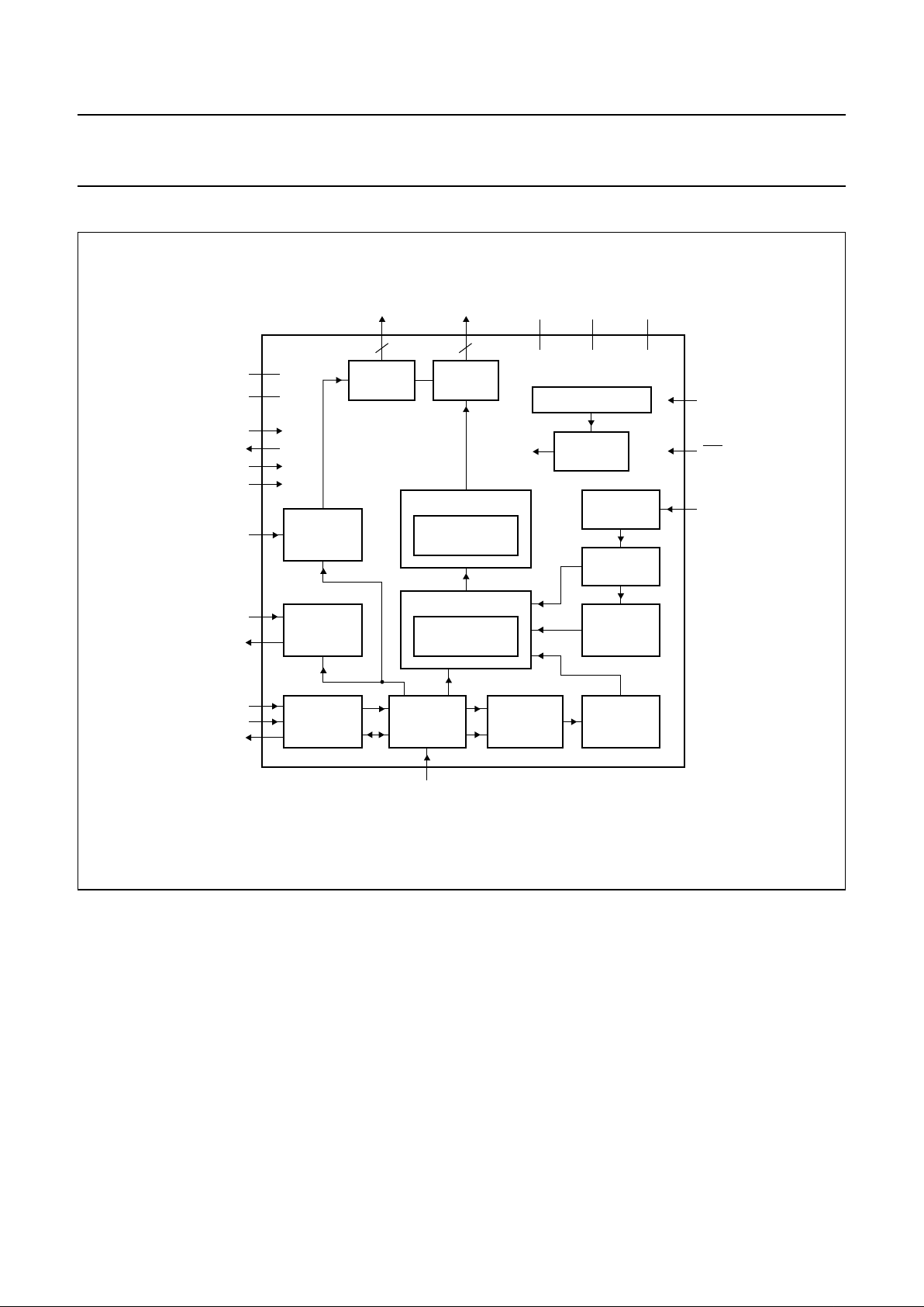
6 BLOCK DIAGRAM
handbook, full pagewidth
MGS465
DISPLAY DATA RAM
MATRIX DATA
RAM
DATA LATCHES
MATRIX
LATCHES
COLUMN
DRIVERS
C0 to C127
PCF8531
R0 to R33
ROW
DRIVERS
COMMAND
DECODER
ADDRESS
COUNTER
DISPLAY
ADDRESS
COUNTER
TIMING
GENERATOR
OSCILLATOR
INTERNAL
RESET
POWER-ON RESET ENR
RES
OSC
I2C-BUS
CONTROL
INPUT
FILTERS
SA0
SCL
SDA
SDACK
V
LCDOUT
V
LCDSENSE
V
LCDIN
T4
T3
T2
T1
34
V
SS2
V
SS1
V
DD1
V
DD2
V
DD3
V
LCD
GENERATOR
BIAS
VOLTAGE
GENERATOR
128
Fig.1 Block diagram.
Page 5

2000 Feb 11 5
Philips Semiconductors Product specification
34 × 128 pixel matrix driver PCF8531
7 PINNING
SYMBOL PAD DESCRIPTION
1 to 14 dummy pads
OSC 15 oscillator input; note 1
V
LCDSENSE
16 voltage multiplier regulation input (V
LCD
); note 2
V
LCDOUT
17 to 23 voltage multiplier output (V
LCD
); note 3
V
LCDIN
24 to 30 LCD supply voltage (V
LCD
); note 2
RES 31 external reset input (active LOW); note 4
V
DD3
32 to 34 supply voltage 3; note 5
V
DD2
35 to 42 supply voltage 2; note 5
V
DD1
43 to 49 supply voltage 1; note 5
SDA 50 and 51 serial data line input of the I
2
C-bus
SDACK 52 serial data acknowledge output; note 6
53 dummy pad
SA0 54 I
2
C-bus slave address input; bit 0
ENR 55 enable internal Power-on reset input; note 7
T4 56 test 4 input; note 8
V
SS2
57 to 63 ground 2; note 9
V
SS1
64 to 70 ground 1; note 9
T3 71 test 3 input; note 8
T1 72 test 1 input; note 8
SCL 73 and 74 serial clock line input of the I
2
C-bus
75 to 77 dummy pads
T2 78 test 2 output; note 10
79 to 86 dummy pads
R0 87 LCD row driver output
R2 88 LCD row driver output
R4 89 LCD row driver output
R6 90 LCD row driver output
R8 91 LCD row driver output
R10 92 LCD row driver output
R12 93 LCD row driver output
R14 94 LCD row driver output
R16 95 LCD row driver output
R18 96 LCD row driver output
R20 97 LCD row driver output
R22 98 LCD row driver output
R24 99 LCD row driver output
R26 100 LCD row driver output
R28 101 LCD row driver output
R30 102 LCD row driver output
R32 103 LCD row driver output
Page 6

2000 Feb 11 6
Philips Semiconductors Product specification
34 × 128 pixel matrix driver PCF8531
Notes
1. If the on-chip oscillator is used, this input must be connected to V
DD1
.
2. If the internal V
LCD
generation is used, V
LCDOUT
, V
LCDIN
and V
LCDSENSE
must be connected together.
3. If an external V
LCD
is used in the application, then pin V
LCDOUT
must be left open circuit, otherwise the chip will be
damaged.
4. If only the internal Power-on reset is used, this input must be connected to V
DD1
.
5. V
DD1
is for the logic supply, V
DD2
, and V
DD3
are for the voltage multiplier. For split power supplies, V
DD2
and V
DD3
must be connected together. If only one supply voltage is available, V
DD1,VDD2
and V
DD3
must be connected
together.
6. Serial data acknowledge for the I2C-bus. By connecting SDACK to SDA externally, the SDA line becomes fully
I2C-bus compatible. Having the acknowledge output separated from the serial data line is advantageous in
Chip-On-Glass (COG) applications. In COG applications where the track resistance from the SDACK pad to the
system SDA line can be significant, a potential divider is generated by the bus pull-up resistor and the Indium Tin
Oxide (ITO) track resistance. It is possible that the PCF8531 will not be able to create a valid logic 0 level during the
acknowledge cycle. By splitting the SDA input from the SDACK output, the device could be used in a mode that
ignores the acknowledge bit. In COG applications where the acknowledge cycle is required, it is necessary to
minimize the track resistance from the SDACK pad to the system SDA line to guarantee a valid LOW level.
7. If ENR is connected to VSS, Power-on reset is disabled; to enable Power-on reset ENR should be connected to V
DD1
.
8. In the application, this input must be connected to VSS.
9. V
SS1
and V
SS2
must be connected together.
10. In the application, T2 must be left open circuit.
C0 to C127 104 to 231 LCD column driver outputs
R33 232 LCD row driver output; icon row
R31 233 LCD row driver output
R29 234 LCD row driver output
R27 235 LCD row driver output
R25 236 LCD row driver output
R23 237 LCD row driver output
R21 238 LCD row driver output
R19 239 LCD row driver output
R17 240 LCD row driver output
R15 241 LCD row driver output
R13 242 LCD row driver output
R11 243 LCD row driver output
R9 244 LCD row driver output
R7 245 LCD row driver output
R5 246 LCD row driver output
R3 247 LCD row driver output
R1 248 LCD row driver output
SYMBOL PAD DESCRIPTION
Page 7

2000 Feb 11 7
Philips Semiconductors Product specification
34 × 128 pixel matrix driver PCF8531
8 FUNCTIONAL DESCRIPTION
8.1 Oscillator
The on-chip oscillator provides the clock signal for the
display system. No external components are required and
the OSC input must be connected to VDD. An external
clock signal, if used, is connected to this input.
8.2 Power-on reset
The on-chip Power-on reset initializes the chip after
Power-on or power failure.
8.3 I
2
C-bus controller
The I2C-bus controller receives and executes the
commands. The PCF8531 acts as an I2C-bus slave
receiver and therefore cannot control bus communication.
8.4 Input filters
To enhance noise immunity in electrically adverse
environments, RC low-pass filters are provided on the
SDA and SCL lines.
8.5 Display data RAM
The PCF8531 contains a 34 × 128 bits static RAM, which
storesthe display data.The RAM is dividedinto 6 banks of
128 bytes (6 × 8 × 128 bits). Bank 6 is used for icon data.
DuringRAM access, datais transferred tothe RAM viathe
I2C-bus interface. There is a direct correspondence
between the X address and column output number.
8.6 Timing generator
The timing generator produces the various signals
required to drive the internal circuitry. Internal chip
operation is notdisturbed by operations on the data buses.
8.7 Address counter
The address counter sets the addresses of the display
data RAM for writing.
8.8 Display address counter
The display address counter generates the addresses for
read out of the display data.
8.9 Command decoder
The command decoder identifies command words that
arrive on the I2C-bus and determines the destination for
the following data bytes.
8.10 Bias voltage generator
The bias voltage generator generates four buffered
intermediate bias voltages. This block contains the
generator for the reference voltages and the four buffers.
This block can operate in two voltage ranges:
• Normal mode; 4.0 to 9.0 V
• Power save mode; 3.0 to 9.0 V.
8.11 V
LCD
generator
The V
LCD
voltage generator contains a configurable
2 to 5 times voltage multiplier; this is software
programmable.
8.12 Reset
The PCF8531 has the possibility of two reset modes,
internal Power-on reset or external reset (
RES). The reset
mode is selected using the ENR signal. After a reset, the
chip has the following state:
• All row and column outputs are set to VSS (display off)
• RAM data is undefined
• Power-down mode.
8.13 Power-down
During power-down, allstatic currents are switched off (no
internal oscillator, no timing and no LCD segment drive
system), and all LCD outputs are internally connected to
VSS. The I2C-bus function remains operational.
8.14 Column driver outputs
The LCD drive section includes 128 column outputs
(C0 to C127) which should be connected directly to the
LCD. The column output signals are generated in
accordance with the multiplexed row signals and with the
data in the display latch. When less than 128 columns are
required, the unused column outputs should be left open
circuit.
8.15 Row driver outputs
The LCD drive section includes 34 row outputs
(R0 to R33), which should be connected directly to the
LCD. The row output signals aregenerated in accordance
with the selected LCD drive mode. If less than 34 rows or
lower Mux rates are required, the unused outputs must be
left open circuit. The row signals are interlaced i.e. the
selection order is R0, R2, ..., R1, R3 etc.
Page 8
2000 Feb 11 8
Philips Semiconductors Product specification
34 × 128 pixel matrix driver PCF8531
8.16 LCD waveforms and DDRAM to data mapping
The LCD waveforms and the DDRAM to display data mapping are shown in Figs 2, 3 and 4.
MGS466
ROW 0
R0 (t)
ROW 2
R2 (t)
COL 0
C0 (t)
COL 1
C1 (t)
0 V
0 V
V3 − V
SS
frame n frame n + 1
02468... 1 35 7... ... 33... 32 02468... 1 3 5 7... ... 33... 32
V
state1
(t)
V
state1
(t)
V
state2
(t)
V
LCD
V
2
V
3
V
4
V
5
V
SS
V
LCD
V
2
V
3
V
4
V
5
V
SS
V
LCD
V
2
V
3
V
4
V
5
V
SS
V
LCD
V
2
V
3
V
4
V
5
V
SS
V
LCD
V
LCD
− V
2
V4 − V
5
VSS − V
5
V4 − V
LCD
V3 − V
2
−V
LCD
0 V
0 V
V3 − V
SS
V
state2
(t)
V
LCD
V
LCD
− V
2
V4 − V
5
V4 − V
LCD
V3 − V
2
VSS − V
5
−V
LCD
Fig.2 Typical LCD driver waveforms.
V
state1
(t) = C1(t) − R0(t).
V
state2
(t) = C1(t) − R2(t).
Page 9
2000 Feb 11 9
Philips Semiconductors Product specification
34 × 128 pixel matrix driver PCF8531
MGS467
ROW 0 to 32
ROW 33
COL 1 on/off
COL 2 off/on
COL 3 on/on
COL 4 off/off
frame n frame n + 1
V
LCD
V
2
V
3
V
4
V
5
V
SS
V
LCD
V
2
V
3
V
4
V
5
V
SS
V
LCD
V
2
V
3
V
4
V
5
V
SS
V
LCD
V
2
V
3
V
4
V
5
V
SS
V
LCD
V
2
V
3
V
4
V
5
V
SS
V
LCD
V
2
V
3
V
4
V
5
V
SS
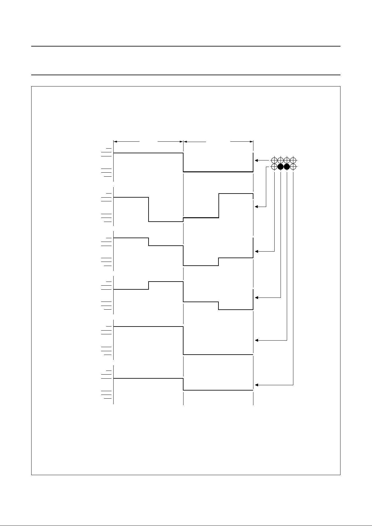
only icons are driven
Fig.3 Icon mode; Mux 1 : 2 LCD waveforms.
Page 10
2000 Feb 11 10
Philips Semiconductors Product specification
34 × 128 pixel matrix driver PCF8531
top of LCD
MGS468
bank 0
bank 1
bank 2
bank 3
bank 4
R32
R24
R16
R8
R0
R33 (icon row)
bank 5
LCD
DDRAM
Fig.4 DDRAM to display mapping.
Page 11
2000 Feb 11 11
Philips Semiconductors Product specification
34 × 128 pixel matrix driver PCF8531
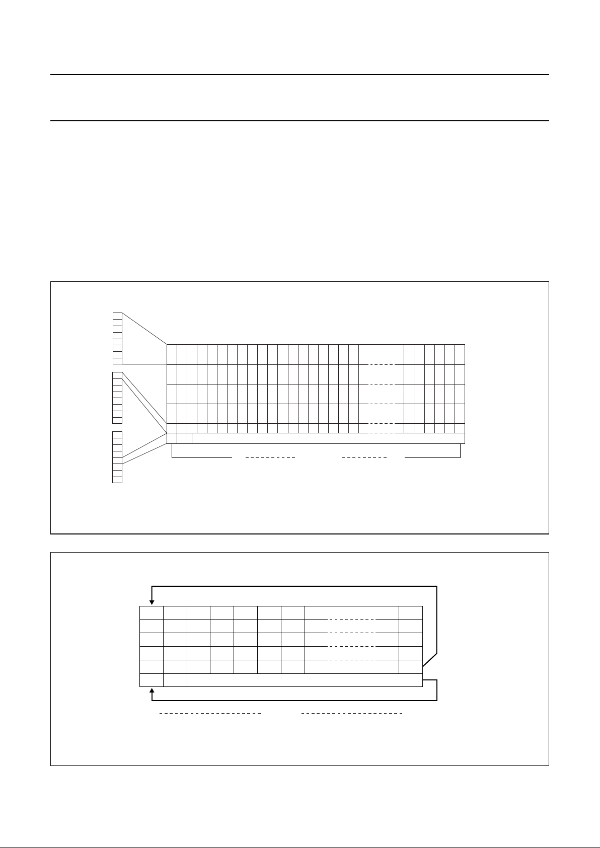
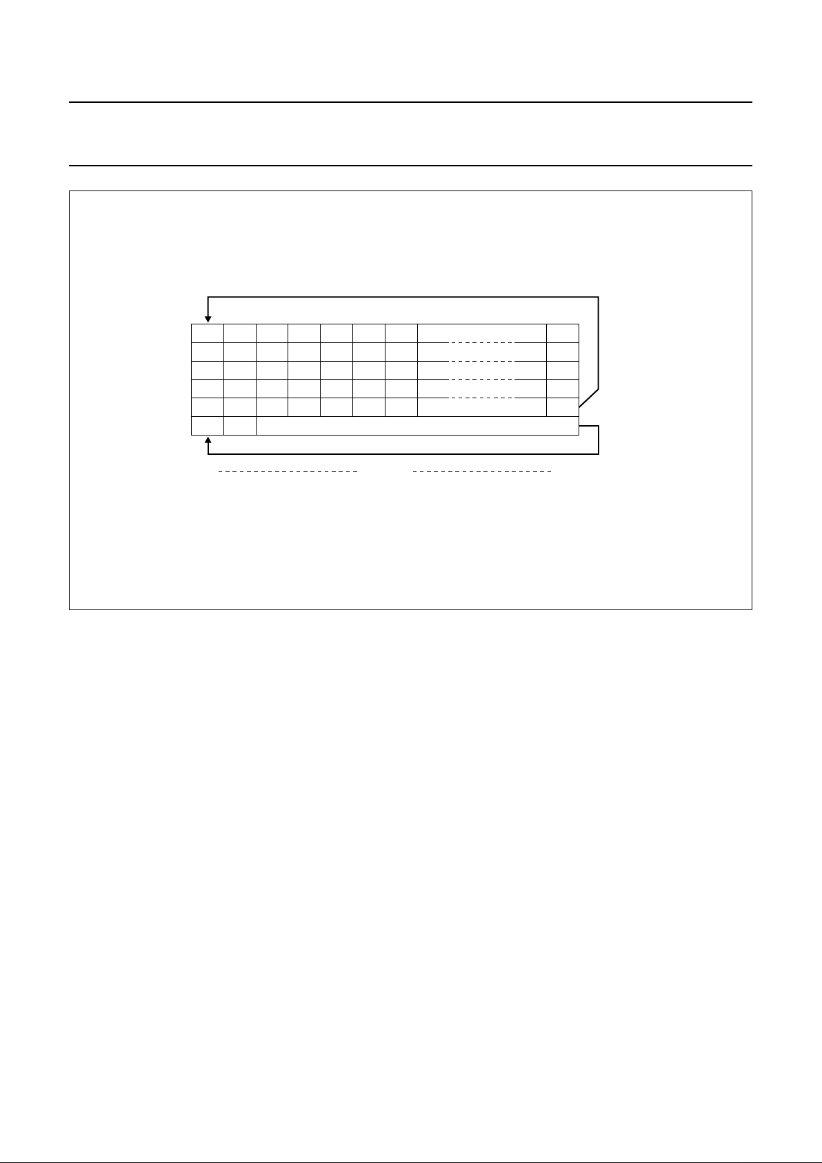
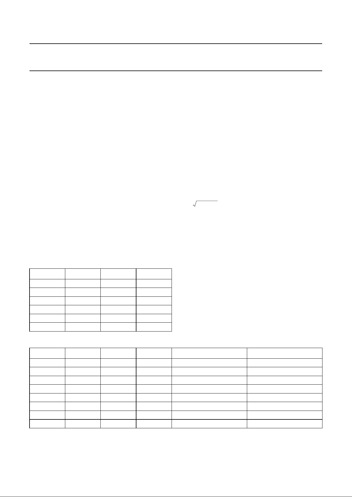
8.17 Addressing
Data is written in bytes into the RAM matrix of the
PCF8531 as illustrated in Figs 5, 6 and 7. The display
RAM has a matrix of 34 × 128 bits. The columns are
addressedbytheaddress pointer. The address rangesare
X 0 to X 127 (7FH) and Y 0 to Y 5 (5H). Addresses
outside of these ranges are not allowed. In vertical
addressing mode (V = 1), the Y address increments after
each byte (see Fig.6). After the last Y address (Y = 4),
Y wraps around to 0 and X increments to address thenext
column. In horizontal addressing mode (V = 0), the
X addressincrements after each byte (seeFig.7).After the
last X address (X = 127), X wraps around to 0 and
Y increments to address the next row. After the very last
address (X = 127 and Y = 4), the address pointers wrap
around to address (X = 0 and Y = 0). It should be noted
thatin bank 4 onlythe LSB (DB0)of the data willbe written
into the RAM. The Y address 5 is reserved for icon data
and is not affected by the addressing mode; it should be
noted that in bank 5 only the 5th data bit (DB4) will be
written into the RAM.
handbook, full pagewidth
MGS469
0
1
2
3
5
4
0 127X address
icon data
Y address
LSB
MSB
LSB
MSB
LSB
MSB
Fig.5 RAM format and addressing.
handbook, full pagewidth
MGS470
05
16
2
3
4
0 1 icon data
0
1
2
3
4
5
638
639
0 127X address
Y address
Fig.6 Sequence of writing data bytes into RAM with vertical addressing (V = 1).
Page 12
2000 Feb 11 12
Philips Semiconductors Product specification
34 × 128 pixel matrix driver PCF8531
handbook, full pagewidth
MGS471
012
128 129 130
256 257 258
384 385 386
512 513 514
0 1 icon data
0
1
2
3
4
5
127
255
383
511
639
0 127X address
Y address
Fig.7 Sequence of writing data bytes into RAM with horizontal addressing (V = 0).
8.18 Instructions
Only two PCF8531 registers, the Instruction Register (IR)
and the Data Register (DR) can be directly controlled by
the MPU. Before internal operation, control information is
stored temporarily in these registers to allow interfacing to
various types of MPUs which operate at different speeds
or to allow interfacing to peripheral control ICs.
The PCF8531 operation is controlled by the instructions
given in Table 1. Details are explained in subsequent
sections.
Instructions are of four types:
1. Those that define PCF8531 functions such as display
configuration, etc.
2. Those that set internal RAM addresses
3. Those that perform data transfer with internal RAM
4. Others.
In normal use, category 3 instructions are used most
frequently. Automatic incrementing by 1 of internal RAM
addressesafter each data write reducestheMPU program
load.
8.18.1 RESET
After reset or internal Power-on reset (depending on
application), the LCD driver will be set to the following
state:
• Power-down mode (PD = 1)
• Horizontal addressing (V = 0)
• Display blank (D = 0; E = 0), no icon mode (IM = 0)
• Address counter X[6:0] = 0; Y[2:0] = 0
• Bias system BS[2:0] = 0
• Multiplex rate M[1:0] = 0 (Mux rate 1 : 17)
• Temperature control mode TC[2:0] = 0
• HV-gen control, HVE = 0 the HV generator is switched
off, PRS = 0 and S[1:0] = 0
• V
LCD
=0V
• RAM data is undefined
• Command page definition H[1:0] = 0.
Page 13
2000 Feb 11 13
Philips Semiconductors Product specification
34 × 128 pixel matrix driver PCF8531
8.18.2 FUNCTION SET
8.18.2.1 PD
When PD = 1, the Power-down mode of the LCD driver is
active:
• All LCD outputs at VSS (display off)
• Power-on reset detection active, oscillator off
• V
LCD
can be disconnected
• I2C-bus is operational, commands can be executed
• RAM contents not cleared; RAM data can be written
• Register settings remain unchanged.
8.18.2.2 V
When V = 0 the horizontal addressing is selected.
The data is written into the DDRAM as shown in Fig.7.
When V = 1 the vertical addressing is selected. The data
is written into the DDRAM as shown in Fig.6. Icon data is
written independently of V when Y address is 5.
8.18.3 SET Y ADDRESS
Bits Y2,Y1and Y0 define the Y address vector of the
display RAM.
Table 1 Yaddress
8.18.4 SET X ADDRESS
The X address points to the columns. The range of X is
0 to 127 (7FH).
8.18.5 SET MULTIPLEX RATE
M[1:0] selects the multiplex rate (see Table 8).
8.18.6 DISPLAY CONTROL (D, E AND IM)
Bits D and E select the display mode (see Table 6). Bit IM
sets the display to icon mode.
8.18.7 SET BIAS SYSTEM
Different multiplex rates require different bias settings.
These are programmed by BS[2:0], which sets the binary
number n. The optimum value for n is given by
Supported values of n are given in Table 2. Table 3shows
the intermediate bias voltages.
Y
2
Y
1
Y
0
BANK
0000
0011
0102
0113
1004
1 0 1 5 (icons)
n Mux rate 3–=
Table 2 Programming the required bias system
BS[2] BS[1] BS[0] n BIAS SYSTEM COMMENT
0007
1
⁄
11
0016
1
⁄
10
0105
1
⁄
9
0114
1
⁄
8
1003
1
⁄
7
recommended for 1 : 34
1012
1
⁄
6
recommended for 1 : 26
1101
1
⁄
5
recommended for 1 : 17
1110
1
⁄
4
recommended for icon mode
Page 14
2000 Feb 11 14
Philips Semiconductors Product specification
34 × 128 pixel matrix driver PCF8531
8.18.8 LCD BIAS VOLTAGE
Table 3 Intermediate LCD bias voltages
8.18.9 S
ET VOPVALUE:
The operating voltage V
LCD
can be set by software.
The voltageat reference temperature[V
LCD
(T = T
cut
)]can
be calculated as: V
LCD
(T
cut
)=(a+VOP× b).
The generated voltage is dependent on the temperature,
programmed Temperature Coefficient (TC) and the
programmed voltage at reference temperature (T
cut
).
V
LCD=VLCD
(T
cut
) × [1+TC×(T − T
cut
)].
The parameter values are given in Table 4.
Two overlapping V
LCD
ranges can be selected via the
command ‘HV-gen control’ (see Table 4 and Fig.8).
The maximum voltage that can be generated depends on
the V
DD2
and V
DD3
voltages and the display load current.
For Mux 1 : 34,the optimum operatingvoltage of theliquid
can be calculated as:
Where V
th
is the threshold voltage of the liquid crystal
material used.
The practical value for VOP is determined by equating
V
off(rms)
with a defined LCD threshold voltage (Vth),
typically when the LCD exhibits approximately
10% contrast.
As the programming range for the internally generated
V
LCD
allows values abovethe maximum allowed V
LCD
, the
user has to ensure, while setting the VOP register and
selecting the temperature compensation, that the V
LCD
limit of maximum 9 V will never be exceeded under all
conditions and including all tolerances.
SYMBOL
BIAS
VOLTAGES
EXAMPLE FOR
1
⁄7BIAS
V1 V
LCD
V
LCD
V2
6
⁄7× V
LCD
V3
5
⁄7× V
LCD
V4
2
⁄7× V
LCD
V5
1
⁄7× V
LCD
V6 V
SS
V
SS
n3+
n4+
------------ -
V
LCD
×
n2+
n4+
------------ -
V
LCD
×
2
n4+
------------ -
V
LCD
×
1
n4+
------------ -
V
LCD
×
V
LCD
134+
21
1
34
----------
–
×
---------------------------------------
V
th
× 5.30 Vth×==
Table 4 Parameter values for the HV generator programming
SYMBOL
VALUE
UNIT
PRS=0 PRS=1
T
cut
27 27 °C
a 2.94 6.75 V
b 0.03 0.03 V
Programming range 2.94 to 6.75 6.75 to 10.56 V
Page 15

2000 Feb 11 15
Philips Semiconductors Product specification
34 × 128 pixel matrix driver PCF8531
handbook, full pagewidth
MGL935
00 01 02
a
V
LCD
03 04 05 06 . . . 7D 7E 7F 00 01 02 03 04 05 06 . . . 5F 6F 7F
b
LOW HIGH
Fig.8 VOP programming of PCF8531.
VOP[6:0] (programmed) [00H to 7FH] programme range LOW and HIGH.
8.18.10 VOLTAGE MULTIPLIER CONTROL S[1:0]
The PCF8531 incorporates a software configurable
voltage multiplier. After reset (internal or external), the
voltage multiplier is set to 2 × V
DD2
. The voltage multiplier
factors are set via the command ‘HV-gen configuration’
(see Tables 4, 5 and 6).
8.18.11 TEMPERATURE COMPENSATION
Due to the temperature dependency of the liquid crystal’s
viscosity, the LCD controlling voltage V
LCD
should usually
be increased at lower temperatures to maintain optimum
contrast. Figure 9 shows V
LCD
for high multiplex rates.
Linear temperature compensation is supported in the
PCF8531. The temperature coefficient of V
LCD
can be
selected from eight values by setting bits TC[2:0]
(see Tables 4, 5 and 6).
handbook, halfpage
MGS473
T
V
LCD
0 °C
Fig.9 V
LCD
as a function of liquid crystal
temperature.
Page 16

2000 Feb 11 16
Philips Semiconductors Product specification
34 × 128 pixel matrix driver PCF8531
Table 5 Instruction set
Note
1. R/
W is set in the slave address byte; Co and RS are set in the control byte.
INSTRUCTION
I
2
C-BUS
COMMAND
(1)
I2C-BUS COMMAND BYTE
DESCRIPTION
RS R/W DB7 DB6 DB5 DB4 DB3 DB2 DB1 DB0
H1 and H0= don’t care (H independent command page)
NOP 0 000000000no operation
Write data 1 0 D
7
D
6
D
5
D
4
D
3
D
2
D
1
D0write data to display RAM
Set default H[1:0] 0 0 0 0000001select H[1:0] = 0
H
1
= 0 and H0= 0 (function and RAM command page)
Instruction set 0 0 0 00010H1H0select command page
Function set 0 0 0 0100PDV0power-down control;
entry mode
Set Yaddress of
RAM
0 001000Y
2
Y
1
Y
0
set Yaddress of RAM;
0 ≤ Y ≤ 5
Set X address of
RAM
001X
6
X
5
X
4
X
3
X
2
X
1
X
0
set X address part of
RAM; 0 ≤ X ≤ 127
H1= 0 and H0= 1 (display setting command page)
Multiplex rate 0 0 0 00001M1M0select multiplex rate
Display control 0 0 0 0001DIMEset display configuration
Bias system 0 0 0 0010BS
2BS1
BS0set Bias System (BSx)
H1= 1 and H0= 0 (HV-gen command page)
HV-gen control 0 0 0 00001PRSHVEset V
LCD
programming
range
HV-gen
configuration
0 0000010S1S0set voltage multiplication
factor
Temperature control 0 0 0 0100TC
2TC1
TC0set temperature
coefficient
Test modes 0 0 0 1 X XXXXXdo not use (reserved for
test)
V
LCD
control 0 0 1 V
OP6VOP5VOP4VOP3VOP2VOP1VOP0
set V
LCD
register
0 ≤ VOP≤ 127
Page 17

2000 Feb 11 17
Philips Semiconductors Product specification
34 × 128 pixel matrix driver PCF8531
Table 6 Explanations for symbols in Table 5
Note
1. The H-bits identify the command page (use set default H[1:0] command to set H[1:0] = 0.
BIT 0 1
PD chip is active chip is in Power-down mode
V horizontal addressing vertical addressing
IM normal mode; full display + icons icon mode; only icons are displayed
H[1:0]
(1)
see Table 7
D and E see Table 7
HVE voltage multiplier disabled voltage multiplier enabled
PRS V
LCD
programming range LOW V
LCD
programming range HIGH
TC[2:0] see Table 7
S[1:0] see Table 7
Table 7 Description of bits H, D and E, TC and S Table 8 Multiplex rates
BITS VALUE DESCRIPTION
Command page (H)
H[1:0] 00 function and RAM command page
01 display setting command page
10 HV-gen command page
Display modes (D, E)
D and E 00 display blank
10 normal mode
01 all display segments
11 inverse video mode
Temperature coefficient (TC)
TC[2:0] 000 temperature coefficient 0
001 temperature coefficient 1
010 temperature coefficient 2
011 temperature coefficient 3
100 temperature coefficient 4
101 temperature coefficient 5
110 temperature coefficient 6
111 temperature coefficient 7
Voltage multiplier factor (S)
S[1:0] 00 2 × voltage multiplier
01 3 × voltage multiplier
10 4 × voltage multiplier
11 5 × voltage multiplier
MUX RATE M1 M0
1:17 0 0
1:26 1 0
1:34 0 1
Page 18

2000 Feb 11 18
Philips Semiconductors Product specification
34 × 128 pixel matrix driver PCF8531
9I2C-BUS INTERFACE
9.1 Characteristics of the I
2
C-bus
The I2C-bus is for bi-directional, two-line communication
between different ICs or modules. The two lines are a
Serial Data line (SDA) and a Serial Clock line (SCL). Both
lines must be connected to a positive supply via a pull-up
resistor. Data transfer may be initiated only when the bus
is not busy.
9.1.1 B
IT TRANSFER
One data bit is transferred during each clock pulse.
The data on the SDA line must remain stable during the
HIGH period of the clock pulse as changes in the data line
at this time will be interpreted as a control signal (see
Fig.10).
9.1.2 START AND STOP CONDITIONS
Bothdata and clock linesremain HIGH when thebus is not
busy. A HIGH-to-LOW transition of the data line, while the
clock is HIGH is defined as the START condition (S).
A LOW-to-HIGH transition of the data line while the clock
is HIGH isdefined asthe STOP condition (P). The START
and STOP conditions are illustrated in Fig.11.
9.1.3 SYSTEM CONFIGURATION
The system configuration is illustrated in Fig.12
• Transmitter: the device that sends the data to the bus
• Receiver: the device that receives the data from the bus
• Master: the device that initiates a transfer, generates
clock signals and terminates a transfer
• Slave: the device addressed by a master
• Multi-Master: more than one master can attempt to
control the bus at the same time without corrupting the
message
• Arbitration: procedure to ensure that, if more than one
master simultaneously tries to control the bus, only one
is allowed to do so and the message is not corrupted
• Synchronization: procedure to synchronize the clock
signals of two or more devices.
9.1.4 A
CKNOWLEDGE
Acknowledge on the I2C-bus is illustrated in Fig.13. Each
byte of eight bits is followed by an acknowledge bit.
The acknowledge bit is a HIGH signal put on the bus by
thetransmitter, during whichtime the mastergenerates an
extra acknowledge related clock pulse. A slave receiver
that is addressedmust generate an acknowledge after the
reception of each byte.
Also, a master receiver must generate an acknowledge
after the reception of each byte that has been clocked out
of the slave transmitter. The device that acknowledges
mustpull-down the SDA line duringtheacknowledge clock
pulse so that the SDA line is stable LOW during the HIGH
periodof the acknowledge- relatedclock pulse (set-up and
hold times must be taken into consideration). A master
receiver must signal an “end of data” to the transmitter by
not generating an acknowledge on the last byte that has
been clocked outof the slave. In this event, thetransmitter
must leave the data line HIGH to enable the master to
generate a STOP condition.
Fig.10 Bit transfer.
handbook, full pagewidth
MBC621
data line
stable;
data valid
change
of data
allowed
SDA
SCL
Page 19

2000 Feb 11 19
Philips Semiconductors Product specification
34 × 128 pixel matrix driver PCF8531
Fig.11 Definition of START and STOP conditions.
handbook, full pagewidth
MBC622
SDA
SCL
P
STOP condition
SDA
SCL
S
START condition
Fig.12 System configuration.
MGA807
SDA
SCL
MASTER
TRANSMITTER/
RECEIVER
MASTER
TRANSMITTER
SLAVE
TRANSMITTER/
RECEIVER
SLAVE
RECEIVER
MASTER
TRANSMITTER/
RECEIVER
Fig.13 Acknowledge on the I2C-bus.
handbook, full pagewidth
MBC602
S
START
condition
9821
clock pulse for
acknowledgement
not acknowledge
acknowledge
DATA OUTPUT
BY TRANSMITTER
DATA OUTPUT
BY RECEIVER
SCL FROM
MASTER
Page 20

2000 Feb 11 20
Philips Semiconductors Product specification
34 × 128 pixel matrix driver PCF8531
9.2 I2C-bus protocol
This driver does not support ‘read’. The PCF8531 is a
slave receiver. Therefore, it only responds when R/W=0
in the slave address byte.
Before any data is transmitted on the I2C-bus, the device
that should respond is addressed first. Two 7-bit slave
addresses (0111100 and 0111101) are reserved for the
PCF8531. The least significant bit of the slave address is
set by connecting the input SA0 to either logic 0 (VSS) or
logic 1 (VDD).
The I2C-bus protocol is illustrated in Fig.14.
The sequence is initiated with a START condition (S) from
the I2C-bus master, and is followed by the slave address.
All slaves with the corresponding address acknowledge in
parallel, all others ignore the I2C-bus transfer. After
acknowledgement, one or more command words follow,
which define the status of the addressed slaves.
A command word consists of a control byte, which defines
Co and RS, plus a data byte (see Fig.14 and Table 1).
The last control byte is tagged with a cleared most
significantbit,thecontinuation bit Co. The control anddata
bytes are also acknowledged by all addressed slaves on
the bus.
After the lastcontrol byte, dependingon the RS bitsetting,
either a series of display data bytes or command data
bytes may follow. If the RS bit was set to logic 1, these
display bytes are stored in the display RAM atthe address
specified by the data pointer.
The data pointer is automatically updated and the data is
directed to the intended PCF8531 device. If the RS bit of
the last control byte was set to logic 0, these command
bytes will be decoded and the setting of the device will be
changed according to the received commands.
The acknowledgementafter each byteis made onlyby the
addressed PCF8531. At the end of the transmission, the
I
2
C-bus master issues a STOP condition (P).
9.3 Command decoder
• Pairs of bytes; information in the second byte, the first
byte determines whether information is display or
instruction data
• Stream of information bytes after Co = 0; display or
instruction data, depending on last RS (Register
Selection).
The command decoder identifies command words that
arrive on the I2C-bus. The most significant bit of a control
byte is the continuation bit Co. If this bit is logic 1, it
indicates that onlyone data byte (either command or RAM
data)will follow. If thisbitis logic 0, it indicatesthat a series
of data bytes (either command or RAM data) may follow.
The DB6 bit of a control byte is the RAM data/command
bit RS. When this bit is at logic 1, it indicates that another
RAM data byte will be transferred next. If the bit is at
logic 0, it indicates that another command byte will be
transferred next.
handbook, full pagewidth
MGS474
S011110SA0 A
slave address
R/W
CoRSXXXXXX
control byte
Fig.14 Slave address and control byte.
Page 21

2000 Feb 11 21
Philips Semiconductors Product specification
34 × 128 pixel matrix driver PCF8531
handbook, full pagewidth
MGS475
S011110
S
A
0
0A
acknowledge
from PCF8531
acknowledge
from PCF8531
acknowledge
from PCF8531
acknowledge
from PCF8531
acknowledge
from PCF8531
1
control byte
A data byte data byte
n ≥ 0 bytes
1 byte
slave address
MSB . . . . . . . . . . . LSB
2n ≥ 0 bytes
A
CoCo
0A AP
RS
R/W
control byte
RS
Fig.15 Master transmits to slave receiver; write mode.
10 LIMITING VALUES
In accordance with the Absolute Maximum Rating System (IEC 134); note 1.
Note
1. Parameters are valid over the operating temperature range unless otherwise specified. All voltages referenced to
VSS unless otherwise noted.
11 HANDLING
Inputs and outputs are protected against electrostatic discharge in normal handling. However, to be totally safe, it is
recommended to take normal precautions appropriate to handling MOS devices (see
“Handling MOS Devices”
).
SYMBOL PARAMETER MIN. MAX. UNIT
V
DD1
logic supply voltage −0.5 +5.5 V
V
DD2,VDD3
multiplier supply voltage −0.5 +4.5 V
I
DD
supply current −50 +50 mA
V
LCD
LCD supply voltage −0.5 +9.0 V
I
LCD
LCD supply current −50 +50 mA
I
SS
negative supply current −50 +50 mA
V
I/VO
input/output voltage (any input/output) −0.5 VDD+ 0.5 V
I
I
DC input current −10 +10 mA
I
O
DC output current −10 +10 mA
P
tot
total power dissipation per package − 300 mW
P/out power dissipation per output − 30 mW
T
stg
storage temperature −65 +150 °C
T
j
junction temperature − 150 °C
Page 22

2000 Feb 11 22
Philips Semiconductors Product specification
34 × 128 pixel matrix driver PCF8531
12 DC CHARACTERISTICS
V
DD1
= 1.8 (1.9) to 5.5 V; V
DD2
and V
DD3
= 2.5 to 4.5 V; V
SS1,2
=0V; V
DD1
to V
DD3
≤ V
LCD
≤ 9.0 V;
T
amb
= −40 to +85 °C; unless otherwise specified.
SYMBOL PARAMETER CONDITIONS MIN. TYP. MAX. UNIT
Supplies
V
LCD
LCD supply voltage note 1 4.0 − 9.0 V
icon mode; note 1 3.0 − 9.0 V
V
DD1
logic supply voltage 1.9 − 5.5 V
T
amb
≥−25 °C 1.8 − 5.5 V
V
DD2,VDD3
multiplier supply voltage LCD voltage internally
generated
2.5 − 4.5 V
I
DD
supply current Power-down mode; internal
V
LCD
− 210µA
normal mode; internal V
LCD
;
notes 2 and 3
− 170 350 µA
normal mode; external V
LCD
;
note 2
− 10 50 µA
I
LCD
LCD input current normal mode; external V
LCD
;
notes 2 and 4
− 25 100 µA
icon mode; external V
LCD
;
notes 2 and 5
− 15 70 µA
V
POR
Power-on reset level note 6 0.9 1.2 1.6 V
Logic
V
IL
LOW-level input voltage V
SS
− 0.3VDDV
V
IH
HIGH-level input voltage 0.7VDD− V
DD
V
I
OL
LOW-level output current (SDA) VOL= 0.4 V; VDD= 5 V 3.0 −−mA
I
LI
input leakage current VI=VDD or V
SS
−1 − +1 µA
Column and row outputs
R
o(col)
column output resistance
C0 to C127
note 7 − 12 20 kΩ
R
o(row)
row output resistance R0 to R33 note 7 − 12 20 kΩ
V
bias(col)
bias tolerance C0 to C127 −100 0 +100 mV
V
bias(row)
bias tolerance R0 to R33 −100 0 +100 mV
Page 23

2000 Feb 11 23
Philips Semiconductors Product specification
34 × 128 pixel matrix driver PCF8531
Notes
1. As the programming range for the internally generated V
LCD
allows values above the maximum allowed V
LCD
, the
user has to ensure, while setting the VOPregister and selecting the temperature compensation, that the V
LCD
limit of
maximum 9 V will never be exceeded under all conditions and including all tolerances.
2. LCD outputs are open circuit, inputs at VDD or VSS; bus inactive.
3. V
DD1
to V
DD3
= 2.85 V; V
LCD
= 7.0 V; voltage multiplier = 3 × VDD; f
OSC
= 34 kHz.
4. V
DD1
to V
DD3
= 2.75 V; V
LCD
= 9.0 V; f
OSC
= 34 kHz.
5. V
DD1
to V
DD3
= 2.75 V; V
LCD
= 3.5 V; f
OSC
= 34 kHz.
6. Resets all logic when V
DD1<VPOR
.
7. I
LOAD
≤50 µA; outputs tested one at a time.
8. V
LCD
≤ 7.7 V.
V
LCD
generation
V
LCD(tol)
LCD voltage tolerance, internal
V
LCD
TC1 to TC7; note 8 −−±3.9 %
TC0 LCD voltage temperature
coefficient 0
T
amb
= −20 to +70 °C − 0 − %/°C
TC1 LCD voltage temperature
coefficient 1
T
amb
= −20 to +70 °C −−0.026 − %/°C
TC2 LCD voltage temperature
coefficient 2
T
amb
= −20 to +70 °C −−0.039 − %/°C
TC3 LCD voltage temperature
coefficient 3
T
amb
= −20 to +70 °C −−0.052 − %/°C
TC4 LCD voltage temperature
coefficient 4
T
amb
= −20 to +70 °C −−0.078 − %/°C
TC5 LCD voltage temperature
coefficient 5
T
amb
= −20 to +70 °C −−0.13 − %/°C
TC6 LCD voltage temperature
coefficient 6
T
amb
= −20 to +70 °C −−0.19 − %/°C
TC7 LCD voltage temperature
coefficient 7
T
amb
= −20 to +70 °C −−0.26 − %/°C
T
cut
cut point temperature − 27 −°C
SYMBOL PARAMETER CONDITIONS MIN. TYP. MAX. UNIT
Page 24

2000 Feb 11 24
Philips Semiconductors Product specification
34 × 128 pixel matrix driver PCF8531
13 AC CHARACTERISTICS
V
DD1
= 1.8 to 5.5 V; V
DD2
and V
DD3
= 2.5 to 4.5 V; V
SS1
and V
SS2
=0V; V
DD1
to V
DD3
≤ V
LCD
≤ 9.0 V;
T
amb
= −40 to +85 °C; unless otherwise specified.
Notes
1. f
frame=fclk(ext)
/480; f
OSC
/480.
2. For t
W(RESL)
> 3 ns a reset may be generated.
3. All timing values are valid within the operating supply voltage and ambient temperature range and are referenced to
VILand VIH with an input voltage swing of VSS to VDD.
4. Cb= total capacitance of one bus line in pF.
SYMBOL PARAMETER CONDITIONS MIN. TYP. MAX. UNIT
f
frame
LCD frame frequency (internal clock) VDD= 3.0 V; note 1 40 66 135 Hz
f
OSC
oscillator frequency (not available at any pin) 20 34 65 kHz
f
clk(ext)
external clock frequency 20 − 65 kHz
t
W(RESL)
reset LOW pulse width note 2 300 −−ns
t
SU;RESL
reset LOW pulse set-up time after Power-on −−30 µs
Serial-bus interface; note 3
f
SCL
SCL clock frequency 0 − 400 kHz
t
SCLL
SCL clock LOW period 1.3 −−µs
t
SCLH
SCL clock HIGH period 0.6 −−µs
t
SU;DAT
data set-up time 100 −−ns
t
HD;DAT
data hold time 0 − 0.9 µs
t
r
SCL, SDA rise time note 4 20 + 0.1Cb− 300 ns
t
f
SCL, SDA fall time note 4 20 + 0.1Cb− 300 ns
C
b
capacitive load represented by each bus line −−400 pF
t
SU;STA
set-up time for a repeated START condition 0.6 −−µs
t
HD;STA
start condition hold time 0.6 −−µs
t
SU;STO
set-up time for STOP condition 0.6 −−µs
t
SW
tolerable spike width on bus −−50 ns
t
BUF
bus free time between a STOP and START
condition
1.3 −−µs
handbook, full pagewidth
MGS476
t
W(RESL)
t
SU;RESL
V
IL
V
DD
RES
Fig.16 Reset timing.
Page 25

2000 Feb 11 25
Philips Semiconductors Product specification
34 × 128 pixel matrix driver PCF8531
Fig.17 I2C-bus timing diagram.
dbook, full pagewidth
SDA
MGA728
SDA
SCL
t
SU;STA
t
SU;STO
t
HD;STA
t
BUF
t
LOW
t
HD;DAT
t
HIGH
t
r
t
f
t
SU;DAT
handbook, halfpage
2345
400
200
100
300
MGS477
I
DD
(µA)
V
DD2
and V
DD3
(V)
4 V
V
LCD
= 9 V
7.5 V
Fig.18 IDD, internal V
LCD
generation.
V
DD1
= 2 V; 4 × voltage multiplier; T
amb
=27°C; TC = 0;
BS = 100; no V
LCD
load.
handbook, halfpage
246 10
400
200
100
300
MGS478
8
I
DD
(µA)
V
LCD
(V)
2×
5×
4×
3×
Fig.19 IDD for different multiplication factors.
V
DD1
= 1.8 V; V
DD2
and V
DD3
= 2.6 V; T
amb
=27°C;
f
OSC
= 34 kHz; no V
LCD
load.
Page 26

2000 Feb 11 26
Philips Semiconductors Product specification
34 × 128 pixel matrix driver PCF8531
handbook, halfpage
−50 0 50 100
9
7
6
8
MGS479
TC0
TC1
TC6
TC7
V
LCD
(V)
T (°C)
Fig.20 Temperature coefficient.
V
LCD
= 7.5 V; V
DD1
to V
DD3
= 2.7 V; T
amb
=27°C; no V
LCD
load.
handbook, halfpage
246 10
30
10
0
20
MGS480
8
I
(µA)
V
LCD
(V)
I
LCD
I
DD
Fig.21 IDD and I
LCD
with external V
LCD
.
V
DD1
= 1.8 V; V
DD2
and V
DD3
= 2.5 V; external V
LCD
;
T
amb
=27°C; TC = 0; BS = 100; no V
LCD
load.
handbook, halfpage
02040 80
30
10
0
20
MGS481
60
I
(µA)
f (kHz)
I
LCD
I
DD
Fig.22 IDD and I
LCD
dependent from frequency.
V
DD1
= 2.5 V; V
DD2
and V
DD3
= 2.5 V; external V
LCD
;
T
amb
=27°C; TC = 0; BS = 100; no V
LCD
load.
handbook, halfpage
3
86
82
84
80
78
3.2 4
MGS482
3.4 3.6 3.8
I
DD
(µA)
V
LCD
(V)
Fig.23 Internal V
LCD
, icon mode.
V
DD1
= 1.8 V; V
DD1
= 2.5 V; 2 × voltage multiplier;
T
amb
=27°C; TC = 0; BS = 111; no V
LCD
load.
Page 27

2000 Feb 11 27
Philips Semiconductors Product specification
34 × 128 pixel matrix driver PCF8531
14 APPLICATION INFORMATION
Table 9 Programming example for PCF8531
STEP
SERIAL BUS BYTE
DISPLAY OPERATION
DB7 DB6 DB5 DB4 DB3 DB2 DB1 DB0
1 0 1 1 1 1 0 SA0 0 start; slave address;
R/
W=0
2 1 0 0 0 0 0 0 0 control byte; Co = 1; RS = 0
3 0 0 0 0 0 0 0 1 H[1:0] independent
command; select function
and RAM command page
(H[1:0] = 00)
4 1 0 0 0 0 0 0 0 control byte; Co = 1; RS = 0
5 0 0 1 0 0 0 1 0 functionand RAMcommand
page PD = 0 and V = 1
6 1 0 0 0 0 0 0 0 control byte; Co = 1; RS = 0
7 0 0 0 0 1 0 0 1 functionand RAMcommand
page select display setting
command page H[1:0] = 01
8 1 0 0 0 0 0 0 0 control byte; Co = 1; RS = 0
9 0 0 0 0 1 1 0 0 display setting command
page; set normal mode
(D = 1; IM = 0 and E = 0)
10 1 0 0 0 0 0 0 0 control byte; Co = 1; RS = 0
11 0 0 0 0 0 1 0 1 select Mux rate 1 : 34
12 1 0 0 0 0 0 0 0 control byte; Co = 1; RS = 0
13 0 0 0 0 0 0 0 1 H[2:0] independent
command; select function
and RAM command page
H[1:0] = 00
14 1 0 0 0 0 0 0 0 control byte; Co = 1; RS = 0
15 0 0 0 0 1 0 1 0 functionandRAMcommand
page; select HV-gen
command page H[1:0] = 10
16 1 0 0 0 0 0 0 0 control byte; Co = 1; RS = 0
17 0 0 0 0 1 0 1 1 HV-gen command page;
select voltage multiplication
factor 5 S[1:0] = 11
18 1 0 0 0 0 0 0 0 control byte; Co = 1; RS = 0
19 0 0 1 0 0 0 1 0 HV-gen command page;
select temperature
coefficient 2 TC[2:0] = 010
20 1 0 0 0 0 0 0 0 control byte; Co = 1; RS = 0
Page 28

2000 Feb 11 28
Philips Semiconductors Product specification
34 × 128 pixel matrix driver PCF8531
21 0 0 0 0 0 1 1 1 HV-gen command page;
select high V
LCD
programming range
(PRS = 1); voltage multiplier
off (HVE = 1)
22 1 0 0 0 0 0 0 0 control byte; Co = 1; RS = 0
23 1 0 1 0 0 0 0 0 HV-gen command page; set
V
LCD
= 7.71 V;
VOP[6:0] = 0100000
24 0 1 0 0 0 0 0 0 control byte; Co = 0; RS = 1
25 0 0 0 1 1 1 1 1 data write; Yand X are
initialized to 0 by default, so
they are not set here
26 0 0 0 0 0 1 0 1 data write
27 0 0 0 0 0 1 1 1 data write
28 0 0 0 0 0 0 0 0 data write
29 0 0 0 1 1 1 1 1 data write
30 0 0 0 0 0 1 0 0 data write
STEP
SERIAL BUS BYTE
DISPLAY OPERATION
DB7 DB6 DB5 DB4 DB3 DB2 DB1 DB0
MGS405
MGS406
MGS407
MGS407
MGS409
MGS410
Page 29

2000 Feb 11 29
Philips Semiconductors Product specification
34 × 128 pixel matrix driver PCF8531
31 0 0 0 1 1 1 1 1 data write; last data and
stop transmission
32 0 1 1 1 1 0 SA0 0 repeated start; slave
address; R/
W=0
33 1 0 0 0 0 0 0 0 control byte; Co = 1; RS = 0
34 0 0 0 0 0 0 0 1 H[1:0] independent
command; select function
and RAM command page
H[1:0] = 00
35 1 0 0 0 0 0 0 0 control byte; Co = 1; RS = 0
36 0 0 0 0 1 0 0 1 functionandRAMcommand
page; select display setting
command page H[1:0] = 01
37 1 0 0 0 0 0 0 0 control byte; Co = 1; RS = 0
38 0 0 0 0 0 0 0 1 H[1:0] independent
command; select function
and RAM command page
H[1:0] = 00
STEP
SERIAL BUS BYTE
DISPLAY OPERATION
DB7 DB6 DB5 DB4 DB3 DB2 DB1 DB0
MGS411
MGS411
MGS411
MGS411
MGS411
MGS411
MGS411
MGS411
Page 30

2000 Feb 11 30
Philips Semiconductors Product specification
34 × 128 pixel matrix driver PCF8531
The pinning of the PCF8531 is optimized for single plane wiring e.g. for chip-on-glass display modules. Display size:
34 × 128 pixels.
39 1 0 0 0 0 0 0 0 control byte; Co = 1; RS = 0
40 0 0 0 0 1 1 0 1 display control; set inverse
video mode (D = 1; E = 1
and IM = 0)
41 1 0 0 0 0 0 0 0 control byte; Co = 1; RS = 0
42 1 0 0 0 0 0 0 0 set X address of RAM; set
address to ‘0000000’
43 0 1 0 0 0 0 0 0 control byte; Co = 0; RS = 1
44 0 0 0 0 0 0 0 0 data write
STEP
SERIAL BUS BYTE
DISPLAY OPERATION
DB7 DB6 DB5 DB4 DB3 DB2 DB1 DB0
MGS411
MGS412
MGS412
MGS412
MGS412
MGS414
Page 31

2000 Feb 11 31
Philips Semiconductors Product specification
34 × 128 pixel matrix driver PCF8531
handbook, full pagewidth
MGS483
HOST
MICROPROCESSOR/
MICROCONTROLLER
LCD PANEL
SDA
V
SS1,
V
SS2
V
SS
V
DD(I2C)
V
LCD
V
DD1
to V
DD3
V
SS1, VSS2
SCL
SDA
SCL
SA0
PCF8531
RES
SDACK
R
pu
R
pu
RES
ENR
128 column drivers
34 row drivers
Fig.24 Typical system configuration.
The host microprocessor/microcontroller and the PCF8531 are both connected to the I2C-bus. The SDA and SCL lines
must be connected to the positive power supply via pull-up resistors. The internal oscillator requires no external
components. The appropriate intermediate biasing voltage for the multiplexed LCD waveforms are generated on-chip.
The only other connections required to complete the system are to the power supplies (VDD,VSSand V
LCD
) and suitable
capacitors for decoupling V
LCD
and VDD.
Page 32

2000 Feb 11 32
Philips Semiconductors Product specification
34 × 128 pixel matrix driver PCF8531
handbook, full pagewidth
MGS484
3
DISPLAY 34 × 128 PIXELS
V
DD1
to
V
DD3
I/O
V
SS1
V
SS2
C
ext
R
supply
R
I/O
V
LCD
PCF8531
12817 17
Fig.25 Chip-on-glass application.
The required minimum values for the external capacitors in an application with the PCF8531 are as follows:
• C
ext
= 100 nF for V
LCD
and V
SS1
and V
SS2
, and C
ext
= 470 nF for V
DD1
to V
DD3
and V
SS1
and V
SS2
• Higher capacitor values are recommended for ripple reduction
• For COG applications, the recommended ITO track resistance is to be minimized for the I/O and supply connections.
Optimized values for these tracks are below 50 Ω for the supply (R
supply
) and below 100 Ω for the I/O connections
(R
I/O
).
• To reduce the sensitivity of the reset to ESD/EMC disturbances for a chip-on-glass application, it is strongly
recommended to implement a series input resistance in the reset line (recommended minimum value 8 kΩ) on the
glass (ITO). If the reset input is not used, it should be connected to V
DD1
using a short connection.
Page 33

2000 Feb 11 33
Philips Semiconductors Product specification
34 × 128 pixel matrix driver PCF8531
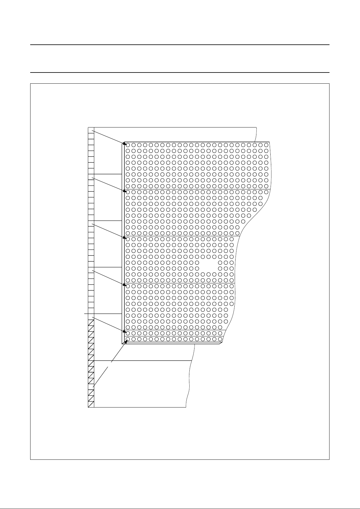
15 BONDING PAD LOCATIONS
Table 10 Bonding pad locations
All x and y coordinates are referenced to the centre of the
chip (dimensions in µm; see Fig.28).
SYMBOL PAD x y
dummy 1 +5973.6 −821.7
dummy 2 +5969.5 +823.4
dummy 3 +5899.5 +823.4
dummy 4 +5829.5 +823.4
dummy 5 +5479.5 +823.4
dummy 6 +5409.5 +823.4
dummy 7 +5059.5 +823.4
dummy 8 +4989.5 +823.4
dummy 9 +4639.5 +823.4
dummy 10 +4569.5 +823.4
dummy 11 +4219.5 +823.4
dummy 12 +4149.5 +823.4
dummy 13 +3799.5 +823.4
dummy 14 +3729.5 +823.4
OSC 15 +3449.5 +823.4
V
LCDSENSE
16 +3169.5 +823.4
V
LCDOUT
17 +3099.5 +823.4
V
LCDOUT
18 +3029.5 +823.4
V
LCDOUT
19 +2959.5 +823.4
V
LCDOUT
20 +2889.5 +823.4
V
LCDOUT
21 +2819.5 +823.4
V
LCDOUT
22 +2749.5 +823.4
V
LCDOUT
23 +2679.5 +823.4
V
LCDIN
24 +2539.5 +823.4
V
LCDIN
25 +2469.5 +823.4
V
LCDIN
26 +2399.5 +823.4
V
LCDIN
27 +2329.5 +823.4
V
LCDIN
28 +2259.5 +823.4
V
LCDIN
29 +2189.5 +823.4
V
LCDIN
30 +2119.5 +823.4
RES 31 +1979.5 +823.4
V
DD3
32 +1699.5 +823.4
V
DD3
33 +1629.5 +823.4
V
DD3
34 +1559.5 +823.4
V
DD2
35 +1279.5 +823.4
V
DD2
36 +1209.5 +823.4
V
DD2
37 +1139.5 +823.4
V
DD2
38 +1069.5 +823.4
V
DD2
39 +999.5 +823.4
V
DD2
40 +929.5 +823.4
V
DD2
41 +859.5 +823.4
V
DD2
42 +789.5 +823.4
V
DD1
43 +649.5 +823.4
V
DD1
44 +579.5 +823.4
V
DD1
45 +509.5 +823.4
V
DD1
46 +439.5 +823.4
V
DD1
47 +369.5 +823.4
V
DD1
48 +299.5 +823.4
V
DD1
49 +229.5 +823.4
SDA 50 +19.5 +823.4
SDA 51 −50.5 +823.4
SDACK 52 −400.5 +823.4
dummy 53 −750.5 +823.4
SA0 54 −820.5 +823.4
ENR 55 −1100.5 +823.4
T4 56 −1380.5 +823.4
V
SS2
57 −1660.5 +823.4
V
SS2
58 −1730.5 +823.4
V
SS2
59 −1800.5 +823.4
V
SS2
60 −1870.5 +823.4
V
SS2
61 −1940.5 +823.4
V
SS2
62 −2010.5 +823.4
V
SS2
63 −2080.5 +823.4
V
SS1
64 −2220.5 +823.4
V
SS1
65 −2290.5 +823.4
V
SS1
66 −2360.5 +823.4
V
SS1
67 −2430.5 +823.4
V
SS1
68 −2500.5 +823.4
V
SS1
69 −2570.5 +823.4
V
SS1
70 −2640.5 +823.4
T3 71 −2780.5 +823.4
T1 72 −3060.5 +823.4
SCL 73 −3410.5 +823.4
SCL 74 −3480.5 +823.4
dummy 75 −3830.5 +823.4
dummy 76 −4180.5 +823.4
dummy 77 −4530.5 +823.4
T2 78 −4600.5 +823.4
SYMBOL PAD x y
Page 34

2000 Feb 11 34
Philips Semiconductors Product specification
34 × 128 pixel matrix driver PCF8531
dummy 79 −4880.5 +823.4
dummy 80 −4950.5 +823.4
dummy 81 −5230.5 +823.4
dummy 82 −5300.5 +823.4
dummy 83 −5650.5 +823.4
dummy 84 −5720.5 +823.4
dummy 85 −5930.5 +823.4
dummy 86 −5926.4 −821.7
R0 87 −5786.4 −821.7
R2 88 −5716.4 −821.7
R4 89 −5646.4 −821.7
R6 90 −5576.4 −821.7
R8 91 −5506.4 −821.7
R10 92 −5436.4 −821.7
R12 93 −5366.4 −821.7
R14 94 −5296.4 −821.7
R16 95 −5226.4 −821.7
R18 96 −5156.4 −821.7
R20 97 −5086.4 −821.7
R22 98 −5016.4 −821.7
R24 99 −4946.4 −821.7
R26 100 −4876.4 −821.7
R28 101 −4806.4 −821.7
R30 102 −4736.4 −821.7
R32 103 −4666.4 −821.7
C0 104 −4526.4 −821.7
C1 105 −4456.4 −821.7
C2 106 −4386.4 −821.7
C3 107 −4316.4 −821.7
C4 108 −4246.4 −821.7
C5 109 −4176.4 −821.7
C6 110 −4106.4 −821.7
C7 111 −4036.4 −821.7
C8 112 −3966.4 −821.7
C9 113 −3896.4 −821.7
C10 114 −3826.4 −821.7
C11 115 −3756.4 −821.7
C12 116 −3686.4 −821.7
C13 117 −3616.4 −821.7
C14 118 −3546.4 −821.7
C15 119 −3476.4 −821.7
SYMBOL PAD x y
C16 120 −3406.4 −821.7
C17 121 −3336.4 −821.7
C18 122 −3266.4 −821.7
C19 123 −3196.4 −821.7
C20 124 −3126.4 −821.7
C21 125 −3056.4 −821.7
C22 126 −2986.4 −821.7
C23 127 −2916.4 −821.7
C24 128 −2846.4 −821.7
C25 129 −2776.4 −821.7
C26 130 −2706.4 −821.7
C27 131 −2636.4 −821.7
C28 132 −2566.4 −821.7
C29 133 −2496.4 −821.7
C30 134 −2426.4 −821.7
C31 135 −2356.4 −821.7
C32 136 −2216.4 −821.7
C33 137 −2146.4 −821.7
C34 138 −2076.4 −821.7
C35 139 −2006.4 −821.7
C36 140 −1936.4 −821.7
C37 141 −1866.4 −821.7
C38 142 −1796.4 −821.7
C39 143 −1726.4 −821.7
C40 144 −1656.4 −821.7
C41 145 −1586.4 −821.7
C42 146 −1516.4 −821.7
C43 147 −1446.4 −821.7
C44 148 −1376.4 −821.7
C45 149 −1306.4 −821.7
C46 150 −1236.4 −821.7
C47 151 −1166.4 −821.7
C48 152 −1096.4 −821.7
C49 153 −1026.4 −821.7
C50 154 −956.4 −821.7
C51 155 −886.4 −821.7
C52 156 −816.4 −821.7
C53 157 −746.4 −821.7
C54 158 −676.4 −821.7
C55 159 −606.4 −821.7
C56 160 −536.4 −821.7
SYMBOL PAD x y
Page 35

2000 Feb 11 35
Philips Semiconductors Product specification
34 × 128 pixel matrix driver PCF8531
C57 161 −466.4 −821.7
C58 162 −396.4 −821.7
C59 163 −326.4 −821.7
C60 164 −256.4 −821.7
C61 165 −186.4 −821.7
C62 166 −116.4 −821.7
C63 167 −46.4 −821.7
C64 168 +93.6 −821.7
C65 169 +163.6 −821.7
C66 170 +233.6 −821.7
C67 171 +303.6 −821.7
C68 172 +373.6 −821.7
C69 173 +443.6 −821.7
C70 174 +513.6 −821.7
C71 175 +583.6 −821.7
C72 176 +653.6 −821.7
C73 177 +723.6 −821.7
C74 178 +793.6 −821.7
C75 179 +863.6 −821.7
C76 180 +933.6 −821.7
C77 181 +1003.6 −821.7
C78 182 +1073.6 −821.7
C79 183 +1143.6 −821.7
C80 184 +1213.6 −821.7
C81 185 +1283.6 −821.7
C82 186 +1353.6 −821.7
C83 187 +1423.6 −821.7
C84 188 +1493.6 −821.7
C85 189 +1563.6 −821.7
C86 190 +1633.6 −821.7
C87 191 +1703.6 −821.7
C88 192 +1773.6 −821.7
C89 193 +1843.6 −821.7
C90 194 +1913.6 −821.7
C91 195 +1983.6 −821.7
C92 196 +2053.6 −821.7
C93 197 +2123.6 −821.7
C94 198 +2193.6 −821.7
C95 199 +2263.6 −821.7
C96 200 +2403.6 −821.7
C97 201 +2473.6 −821.7
SYMBOL PAD x y
C98 202 +2543.6 −821.7
C99 203 +2613.6 −821.7
C100 204 +2683.6 −821.7
C101 205 +2753.6 −821.7
C102 206 +2823.6 −821.7
C103 207 +2893.6 −821.7
C104 208 +2963.6 −821.7
C105 209 +3033.6 −821.7
C106 210 +3103.6 −821.7
C107 211 +3173.6 −821.7
C108 212 +3243.6 −821.7
C109 213 +3313.6 −821.7
C110 214 +3383.6 −821.7
C111 215 +3453.6 −821.7
C112 216 +3523.6 −821.7
C113 217 +3593.6 −821.7
C114 218 +3663.6 −821.7
C115 219 +3733.6 −821.7
C116 220 +3803.6 −821.7
C117 221 +3873.6 −821.7
C118 222 +3943.6 −821.7
C119 223 +4013.6 −821.7
C120 224 +4083.6 −821.7
C121 225 +4153.6 −821.7
C122 226 +4223.6 −821.7
C123 227 +4293.6 −821.7
C124 228 +4363.6 −821.7
C125 229 +4433.6 −821.7
C126 230 +4503.6 −821.7
C127 231 +4573.6 −821.7
R33 232 +4713.6 −821.7
R31 233 +4783.6 −821.7
R29 234 +4853.6 −821.7
R27 235 +4923.6 −821.7
R25 236 +4993.6 −821.7
R23 237 +5063.6 −821.7
R21 238 +5133.6 −821.7
R19 239 +5203.6 −821.7
R17 240 +5343.6 −821.7
R15 241 +5413.6 −821.7
R13 242 +5483.6 −821.7
SYMBOL PAD x y
Page 36

2000 Feb 11 36
Philips Semiconductors Product specification
34 × 128 pixel matrix driver PCF8531
Table 11 Bonding pads
Table 12 Alignment marks
R11 243 +5553.6 −821.7
R9 244 +5623.6 −821.7
R7 245 +5693.6 −821.7
R5 246 +5763.6 −821.7
R3 247 +5833.6 −821.7
R1 248 +5903.6 −821.7
PAD SIZE UNIT
Pad pitch min. 70 µm
Pad size; Al 62 × 100 µm
Bump dimensions 50 × 90 × 17.5 (±5) µm
Waferthickness (excluding
bumps)
381 µm
MARKS x y
C1 −5402.0 +823.1
C2 +5292.4 +823.4
F +5890.3 +401.9
Circle 1 −5543.0 +798.4
Circle 2 +5637.4 +798.4
SYMBOL PAD x y
handbook, halfpage
MGS487
x
y
12.23 mm
pitch
1.96
mm
PCF8531
Fig.26 Bonding pads.
handbook, full pagewidth
MGS490
x center
C
y
center
100 µm
x center
circle
y
center
100
µm
100
µm
100
µm
x center
F
y
center
80 µm
Fig.27 Shapes of recognition pattern.
Page 37

2000 Feb 11 37
Philips Semiconductors Product specification
34 × 128 pixel matrix driver PCF8531
This text is here in white to force landscape pages to be rotated correctly when browsing through the pdf in the Acrobat reader.This text is here in
_white to force landscape pages to be rotated correctly when browsing through the pdf in the Acrobat reader.This text is here inThis text is here in
white to force landscape pages toberotatedcorrectly when browsing through the pdf in the Acrobat reader. white to force landscape pages to be ...
handbook, full pagewidth
MGS486
pad1
T2
T1
T3
SCL
SDA
OSC
RES
V
SS1VSS2
V
LCDINVLCDOUT
V
LCDSENSE
V
DD1VDD2VDD3
ENR
SA0
SDACK
PC8531-1
T4
x
y
0,0
C63
...
...
C127
...
C64
...
C31
...
C32
...
R32
...C0...
R0
...
C96
C95
...
R33
...
R1
...
Fig.28 Bonding pad location.
The positioning of the bonding pads is not to scale.
Page 38

2000 Feb 11 38
Philips Semiconductors Product specification
34 × 128 pixel matrix driver PCF8531
16 DEVICE PROTECTION DIAGRAM
For all diagrams: the maximum forward current is 5 mA and the maximum reverse voltage is 5 V.
handbook, full pagewidth
MGS485
V
DD1
V
DD1
V
SS1
V
SS2
V
SS1
SCL, SDA, SDACK
V
SS1
V
LCDIN
V
SS1
V
SS1
V
DD1
OSC, SA0, T3, T1, T4, RES, ENR
V
SS1
V
DD1
T2
PADS 43 to 49
PADS 35 to 42
PADS 57 to 63
V
DD3
V
SS1
PADS 32 to 34
V
LCDOUT
V
SS1
PADS 17 to 23
V
LCDIN
(SUPPLY),
V
LCDSENSE
V
SS1
PADS 16, 24 to 30
PADS 87 to 248
PADS 73, 74, 50, 51, 52
PADS 15, 54, 71, 72, 56, 31, 55
PAD 78
PADS 64 to 70
PADS 57 to 63
V
DD2
V
SS1
V
SS2
Fig.29 Device protection diagrams.
Page 39

2000 Feb 11 39
Philips Semiconductors Product specification
34 × 128 pixel matrix driver PCF8531
17 TRAY INFORMATION
handbook, full pagewidth
MGS488
D
C
A
x
y
F
E
B
Fig.30 Tray details.
The dimensions are given in Table 13.
Table 13 Dimensions
handbook, halfpage
MGS489
PC8531-1
Fig.31 Tray alignment.
The orientation of the IC in a pocket is indicated by the position of
the IC type name on the die surface with respect to the chamfer on
the upper left corner of the tray. Refer to the bonding pad location
diagram for the orientating and position of the type name on the die
surface.
DIM. DESCRIPTION VALUE
A pocket pitch; x direction 13.72 mm
B pocket pitch; y direction 4.17 mm
C pocket width; x direction 12.34 mm
D pocket width; y direction 2.05 mm
E tray width; x direction 50.8 mm
F tray width; y direction 50.8 mm
x number of pockets in x direction 3
y number of pockets in y direction 10
Page 40

2000 Feb 11 40
Philips Semiconductors Product specification
34 × 128 pixel matrix driver PCF8531
18 DEFINITIONS
19 LIFE SUPPORT APPLICATIONS
These products are not designed for use in life support appliances, devices, or systems where malfunction of these
products can reasonably be expected to result in personal injury. Philips customers using or selling these products for
use in such applications do so at their own risk and agree to fully indemnify Philips for any damages resulting from such
improper use or sale.
20 PURCHASE OF PHILIPS I
2
C COMPONENTS
Data sheet status
Objective specification This data sheet contains target or goal specifications for product development.
Preliminary specification This data sheet contains preliminary data; supplementary data may be published later.
Product specification This data sheet contains final product specifications.
Limiting values
Limiting values given are in accordance with the Absolute Maximum Rating System (IEC 134). Stress above one or
more of the limiting values may cause permanent damage to the device. These are stress ratings only and operation
of the device at these or at any other conditions above those given in the Characteristics sections of the specification
is not implied. Exposure to limiting values for extended periods may affect device reliability.
Application information
Where application information is given, it is advisory and does not form part of the specification.
Purchase of Philips I
2
C components conveys a license under the Philips’ I2C patent to use the
components in the I2C system provided the system conforms to the I2C specification defined by
Philips. This specification can be ordered using the code 9398 393 40011.
Page 41

2000 Feb 11 41
Philips Semiconductors Product specification
34 × 128 pixel matrix driver PCF8531
NOTES
Page 42

2000 Feb 11 42
Philips Semiconductors Product specification
34 × 128 pixel matrix driver PCF8531
NOTES
Page 43

2000 Feb 11 43
Philips Semiconductors Product specification
34 × 128 pixel matrix driver PCF8531
NOTES
Page 44

© Philips Electronics N.V. SCA
All rights are reserved. Reproduction in whole or in part is prohibited without the prior written consent of the copyright owner.
The information presented in this document does not form part of any quotation or contract, is believed to be accurate and reliable and may be changed
without notice. No liability will be accepted by the publisher for any consequence of its use. Publication thereof does not convey nor imply any license
under patent- or other industrial or intellectual property rights.
Internet: http://www.semiconductors.philips.com
2000
69
Philips Semiconductors – a w orldwide compan y
For all other countries apply to: Philips Semiconductors,
International Marketing & Sales Communications, Building BE-p, P.O. Box 218,
5600 MD EINDHOVEN, The Netherlands, Fax. +31 40 27 24825
Argentina: see South America
Australia: 3 Figtree Drive, HOMEBUSH, NSW 2140,
Tel. +61 2 9704 8141, Fax. +61 2 9704 8139
Austria: Computerstr. 6, A-1101 WIEN, P.O. Box 213,
Tel. +43 1 60 101 1248, Fax. +43 1 60 101 1210
Belarus: Hotel Minsk Business Center, Bld. 3, r. 1211, Volodarski Str. 6,
220050 MINSK, Tel. +375 172 20 0733, Fax. +375 172 20 0773
Belgium: see The Netherlands
Brazil: see South America
Bulgaria: Philips Bulgaria Ltd., Energoproject, 15th floor,
51 James Bourchier Blvd., 1407 SOFIA,
Tel. +359 2 68 9211, Fax. +359 2 68 9102
Canada: PHILIPS SEMICONDUCTORS/COMPONENTS,
Tel. +1 800 234 7381, Fax. +1 800 943 0087
China/Hong Kong: 501 Hong Kong Industrial Technology Centre,
72 Tat Chee Avenue, Kowloon Tong, HONG KONG,
Tel. +852 2319 7888, Fax. +852 2319 7700
Colombia: see South America
Czech Republic: see Austria
Denmark: Sydhavnsgade 23, 1780 COPENHAGEN V,
Tel. +45 33 29 3333, Fax. +45 33 29 3905
Finland: Sinikalliontie 3, FIN-02630 ESPOO,
Tel. +358 9 615 800, Fax. +358 9 6158 0920
France: 51 Rue Carnot, BP317, 92156 SURESNES Cedex,
Tel. +33 1 4099 6161, Fax. +33 1 4099 6427
Germany: Hammerbrookstraße 69, D-20097 HAMBURG,
Tel. +49 40 2353 60, Fax. +49 40 2353 6300
Hungary: see Austria
India: Philips INDIA Ltd, Band Box Building, 2nd floor,
254-D, Dr. Annie Besant Road, Worli, MUMBAI 400 025,
Tel. +91 22 493 8541, Fax. +91 22 493 0966
Indonesia: PTPhilips Development Corporation,SemiconductorsDivision,
Gedung Philips, Jl. Buncit Raya Kav.99-100, JAKARTA 12510,
Tel. +62 21 794 0040 ext. 2501, Fax. +62 21 794 0080
Ireland: Newstead, Clonskeagh, DUBLIN 14,
Tel. +353 1 7640 000, Fax. +353 1 7640 200
Israel: RAPAC Electronics, 7 Kehilat Saloniki St, PO Box 18053,
TEL AVIV 61180, Tel. +972 3 645 0444, Fax. +972 3 649 1007
Italy: PHILIPS SEMICONDUCTORS, Via Casati, 23 - 20052 MONZA (MI),
Tel. +39 039 203 6838, Fax +39 039 203 6800
Japan: Philips Bldg 13-37, Kohnan 2-chome, Minato-ku,
TOKYO 108-8507, Tel. +81 3 3740 5130, Fax. +81 3 3740 5057
Korea: Philips House, 260-199 Itaewon-dong, Yongsan-ku, SEOUL,
Tel. +82 2 709 1412, Fax. +82 2 709 1415
Malaysia: No. 76 Jalan Universiti, 46200 PETALING JAYA, SELANGOR,
Tel. +60 3 750 5214, Fax. +60 3 757 4880
Mexico: 5900 Gateway East, Suite 200, EL PASO, TEXAS 79905,
Tel. +9-5 800 234 7381, Fax +9-5 800 943 0087
Middle East: see Italy
Netherlands: Postbus 90050, 5600 PB EINDHOVEN, Bldg. VB,
Tel. +31 40 27 82785, Fax. +31 40 27 88399
New Zealand: 2 Wagener Place, C.P.O. Box 1041, AUCKLAND,
Tel. +64 9 849 4160, Fax. +64 9 849 7811
Norway: Box 1, Manglerud 0612, OSLO,
Tel. +47 22 74 8000, Fax. +47 22 74 8341
Pakistan: see Singapore
Philippines: Philips Semiconductors Philippines Inc.,
106 Valero St. Salcedo Village, P.O. Box 2108 MCC, MAKATI,
Metro MANILA, Tel. +63 2 816 6380, Fax. +63 2 817 3474
Poland: Al.Jerozolimskie 195 B, 02-222 WARSAW,
Tel. +48 22 5710 000, Fax. +48 22 5710 001
Portugal: see Spain
Romania: see Italy
Russia: Philips Russia, Ul. Usatcheva 35A, 119048 MOSCOW,
Tel. +7 095 755 6918, Fax. +7 095 755 6919
Singapore: Lorong 1, Toa Payoh, SINGAPORE 319762,
Tel. +65 350 2538, Fax. +65 251 6500
Slovakia: see Austria
Slovenia: see Italy
South Africa: S.A. PHILIPS Pty Ltd., 195-215 Main Road Martindale,
2092 JOHANNESBURG, P.O. Box 58088 Newville 2114,
Tel. +27 11 471 5401, Fax. +27 11 471 5398
South America: Al. Vicente Pinzon, 173, 6th floor,
04547-130 SÃO PAULO, SP, Brazil,
Tel. +55 11 821 2333, Fax. +55 11 821 2382
Spain: Balmes 22, 08007 BARCELONA,
Tel. +34 93 301 6312, Fax. +34 93 301 4107
Sweden: Kottbygatan 7, Akalla, S-16485 STOCKHOLM,
Tel. +46 8 5985 2000, Fax. +46 8 5985 2745
Switzerland: Allmendstrasse 140, CH-8027 ZÜRICH,
Tel. +41 1 488 2741 Fax. +41 1 488 3263
Taiwan: Philips Semiconductors, 6F, No. 96, Chien Kuo N. Rd., Sec. 1,
TAIPEI, Taiwan Tel. +886 2 2134 2886, Fax. +886 2 2134 2874
Thailand: PHILIPS ELECTRONICS (THAILAND) Ltd.,
209/2 Sanpavuth-Bangna Road Prakanong, BANGKOK 10260,
Tel. +66 2 745 4090, Fax. +66 2 398 0793
Turkey: Yukari Dudullu, Org. San. Blg., 2.Cad. Nr. 28 81260 Umraniye,
ISTANBUL, Tel. +90 216 522 1500, Fax. +90 216 522 1813
Ukraine: PHILIPS UKRAINE, 4 Patrice Lumumba str., Building B, Floor 7,
252042 KIEV, Tel. +380 44 264 2776, Fax. +380 44 268 0461
United Kingdom: Philips Semiconductors Ltd., 276 Bath Road, Hayes,
MIDDLESEX UB3 5BX, Tel. +44 208 730 5000, Fax. +44 208 754 8421
United States: 811 East Arques Avenue, SUNNYVALE, CA 94088-3409,
Tel. +1 800 234 7381, Fax. +1 800 943 0087
Uruguay: see South America
Vietnam: see Singapore
Yugoslavia: PHILIPS, Trg N. Pasica 5/v, 11000 BEOGRAD,
Tel. +381 11 3341 299, Fax.+381 11 3342 553
Printed in The Netherlands 465006/03/pp44 Date of release: 2000 Feb 11 Document order number: 9397 750 06616
 Loading...